EP1933416A1 - Module d'antenne intégrée - Google Patents
Module d'antenne intégrée Download PDFInfo
- Publication number
- EP1933416A1 EP1933416A1 EP07023678A EP07023678A EP1933416A1 EP 1933416 A1 EP1933416 A1 EP 1933416A1 EP 07023678 A EP07023678 A EP 07023678A EP 07023678 A EP07023678 A EP 07023678A EP 1933416 A1 EP1933416 A1 EP 1933416A1
- Authority
- EP
- European Patent Office
- Prior art keywords
- circuit board
- top plate
- antenna
- integrated module
- antenna element
- Prior art date
- Legal status (The legal status is an assumption and is not a legal conclusion. Google has not performed a legal analysis and makes no representation as to the accuracy of the status listed.)
- Withdrawn
Links
Images
Classifications
-
- H—ELECTRICITY
- H01—ELECTRIC ELEMENTS
- H01Q—ANTENNAS, i.e. RADIO AERIALS
- H01Q1/00—Details of, or arrangements associated with, antennas
- H01Q1/08—Means for collapsing antennas or parts thereof
- H01Q1/088—Quick-releasable antenna elements
-
- H—ELECTRICITY
- H01—ELECTRIC ELEMENTS
- H01Q—ANTENNAS, i.e. RADIO AERIALS
- H01Q1/00—Details of, or arrangements associated with, antennas
- H01Q1/12—Supports; Mounting means
- H01Q1/22—Supports; Mounting means by structural association with other equipment or articles
- H01Q1/24—Supports; Mounting means by structural association with other equipment or articles with receiving set
- H01Q1/241—Supports; Mounting means by structural association with other equipment or articles with receiving set used in mobile communications, e.g. GSM
- H01Q1/242—Supports; Mounting means by structural association with other equipment or articles with receiving set used in mobile communications, e.g. GSM specially adapted for hand-held use
- H01Q1/243—Supports; Mounting means by structural association with other equipment or articles with receiving set used in mobile communications, e.g. GSM specially adapted for hand-held use with built-in antennas
-
- H—ELECTRICITY
- H01—ELECTRIC ELEMENTS
- H01Q—ANTENNAS, i.e. RADIO AERIALS
- H01Q1/00—Details of, or arrangements associated with, antennas
- H01Q1/44—Details of, or arrangements associated with, antennas using equipment having another main function to serve additionally as an antenna, e.g. means for giving an antenna an aesthetic aspect
-
- H—ELECTRICITY
- H01—ELECTRIC ELEMENTS
- H01Q—ANTENNAS, i.e. RADIO AERIALS
- H01Q1/00—Details of, or arrangements associated with, antennas
- H01Q1/52—Means for reducing coupling between antennas; Means for reducing coupling between an antenna and another structure
-
- H—ELECTRICITY
- H01—ELECTRIC ELEMENTS
- H01Q—ANTENNAS, i.e. RADIO AERIALS
- H01Q9/00—Electrically-short antennas having dimensions not more than twice the operating wavelength and consisting of conductive active radiating elements
- H01Q9/04—Resonant antennas
- H01Q9/0407—Substantially flat resonant element parallel to ground plane, e.g. patch antenna
- H01Q9/0421—Substantially flat resonant element parallel to ground plane, e.g. patch antenna with a shorting wall or a shorting pin at one end of the element
Definitions
- the present invention relates to an antenna-integrated module suitable for a small-sized transceiver used for communication or broadcasting.
- each transceiver unit is an antenna-integrated high frequency module in which an antenna element is mounted on a circuit board with a high frequency circuit.
- a sheet-metal shield case covers a predetermined region of the circuit board on which the main elements of the high frequency circuit are mounted.
- An antenna element such as a chip antenna or a pattern antenna is mounted on other regions of the circuit board (for example, see JP-A-2002-232221 (pages 4 to 6 and Fig. 1 )).
- the size of the entire module increases in plan view. Therefore, a problem arises in that it is difficult to decrease the size thereof. Moreover, if a configuration in which the chip antenna is used as the antenna element and connected to the high frequency circuit through a coaxial cable is used, a problem also arises in that element cost considerably increases.
- a shield case for electrically shielding circuit elements of a high frequency circuit also serves as an antenna element of an inverted F-type antenna (for example, see JP-A-2005-5866 (pages 4 and 5 and Fig. 1 )).
- a sheet-metal covering antenna element including a plurality of bent leg pieces extend from the periphery of a rectangular top plate (flat metal plate). The covering antenna element is mounted on a circuit board with a high frequency circuit.
- a predetermined bent leg piece is connected to a wiring pattern of the high frequency circuit or a ground conductive layer so as to serve as a feeding pin or a short-circuited pin and the remaining bent leg pieces are also connected to an electrically isolated soldering land.
- the top plate stably supported by the bent leg pieces is disposed so as to be opposite the circuit board at a predetermined interval at a position where the top plate covers the circuit elements of the high frequency circuit. Therefore, the top plate connected to the bent leg piece corresponding to the short-circuited pin can electrically shield the circuit elements of the high frequency circuit. Since the top plate is connected to the bent leg piece corresponding to the feeding pin, the top plate can serve as a radiation conductor of an inverted F-type antenna.
- the sheet-metal covering antenna element it is possible to realize antenna-integrated module that can be easily miniaturized and manufactured at low cost, compared with the known technique in which a special antenna element and a shield case are disposed in line in plan view.
- the covering antenna element is used to decrease the size thereof and manufacture it at low cost.
- the top plate formed of the metal plate is disposed at a position where the top plate covers the circuit elements. Accordingly, when a reflow soldering process of the circuit elements mounted on the circuit board and a reflow soldering process of the covering antenna element are performed together, heat cannot be sufficiently delivered from a reflow furnace to a region covered with the top plate. Therefore, the soldering connection of the circuit elements may deteriorate.
- the covering antenna element is mounted on the circuit board, and then the reflow soldering process has to be performed again at lower melting temperature than the temperature in the first reflow soldering process. Therefore, a problem arises in that the reflow process cannot be effectively performed.
- a plurality of the bent leg pieces just extend from the periphery of the top plate, and thus a space (region on which circuit elements are mounted) covered with the top plate is considerably exposed in side view. Therefore, a soldering iron or the like may be inserted from the side of the space, and thus arbitrary alteration of major elements of the high frequency may occur.
- the present invention is designed to solve the above-described problems, and an object of the invention is to provide an antenna-integrated module capable of easily decreasing the size thereof, preventing arbitrary alternation of a circuit, effectively performing a reflow process, and being manufactured at low cost.
- an antenna-integrated module including: a circuit board on which a wiring pattern and a ground conductive layer of a high frequency circuit are disposed; circuit elements which are mounted on one surface of the circuit board; and a sheet-metal covering antenna element which is mounted on the circuit board to cover the circuit elements, wherein the covering antenna element has a top plate which is opposite the circuit board with a predetermined space and serves as a radiation conductor, a power feeding leg piece which extends from a feeding point of the top plate to the circuit board to be connected to the wiring pattern, a short-circuited leg piece which extends from the periphery of one end of the top plate to the circuit board to be connected to the ground conductive layer, a support leg piece which extends from the periphery of the other end of the top plate to the circuit board to be fixed on the circuit board so as to be electrically opened, and side plates which extend at positions other than the power feeding leg piece, the short-circuited leg piece, and the support leg piece from the
- the antenna-integrated module having the above-described configuration can serve as a shield chase for electrically shielding the circuit elements of the high frequency circuit and can also serve as an antenna element of an inverted F-type metal plate antenna by using the top plate as a radiation conductor. Accordingly, it is possible to decrease the size of the entire module and decrease manufacturing cost, compared with a configuration in which a special antenna element and a shield case are disposed in line in plan view. Since the openings are formed at a plurality of positions of the top plate and air can be circulated through the openings, heat can be easily delivered to the region of the circuit board covered with the covering antenna element in the reflow process.
- the reflow soldering process of the circuit elements mounted on the circuit board and the reflow soldering process of the covering antenna element can be performed together.
- the openings are formed in the slit shape or the small hole shape, it is difficult to inserting a soldering iron or the like into the openings.
- the side plates extend from the periphery of the top plate to the circuit board, it is also difficult to insert the soldering iron or the like into the space covered with the covering antenna element from the side. Therefore, it is difficult to arbitrarily alter the major part of the high frequency circuit of the antenna-integrated module.
- the slit-like or small hole-like openings may be formed at a plurality of positions spaced from the periphery of the side plates. In this case, preferably, heat can be more easily delivered to the region of the circuit board covered with the covering antenna element in the reflow process.
- the top plate may have a rectangular shape, and the short-circuited leg pieces may extend from two positions of one end of the top plate in a longitudinal direction of the top plate and the support leg pieces extend from two positions of the other end of the top plate in the longitudinal direction.
- the shape of the covering antenna element can be simplified, the manufacturing is preferably facilitated.
- a third support leg piece having the same shape as the power feeding leg piece may be formed at a position point-symmetrical to the power feeding leg piece, so that the covering antenna element has the symmetrical shape of which the outer appearance is not different even when both ends of the covering antenna element in the longitudinal direction is reversed. In a manufacturing process of mounting the covering antenna element on the circuit board, it is not necessary to check the direction of the antenna element, thereby improving working efficiency.
- the circuit board may be configured to be inserted into or extracted from a connector and the connector has guide pieces which interpose both side portions of the circuit board in a thickness direction of the circuit board, and when the circuit board may be inserted into the connector to be connected to the connector, the guide pieces are located in the gaps extending along a direction of the insertion of the circuit board between the side plates and the circuit board. Since the side plate of the covering antenna element can be prevented from coming in contact with the guide pieces of the connector, the top plate of the covering antenna element can be expanded so as to have the same size as the width size of the circuit board, and moreover the limited space of the circuit board can be effectively used as an element-mounted region.
- the top plate may have a rectangular shape, and the short-circuited leg pieces may extend from two positions of one end of the top plate in a transverse direction of the top plate, the support leg pieces extend from two positions of the other end of the top plate in the transverse direction, and the gaps are formed over the entire lengths of the side plates extending from both ends of the top plate in a longitudinal direction of the top plate. Since the shape of the covering antenna element can be simplified, the manufacturing is facilitated. Moreover, it is possible to insert the circuit board into the connector.
- the width sizes of the openings and distances between the front ends of the support leg pieces and the circuit board opposed to each other may be all set to 1 mm or less. It is possible to preferably prevent arbitrary alternation of the major part of the high frequency circuit.
- An antenna-integrated module having the above-described configuration can serve as a shield chase for electrically shielding the circuit elements of the high frequency circuit and can also serve as an antenna element of an inverted F-type antenna by using the top plate as a radiation conductor. Accordingly, it is possible to decrease the size of the entire module and decrease manufacturing cost, compared with a configuration in which a special antenna element and a shield case are disposed in line in plan view. Since the openings are formed at a plurality of positions of the top plate and air can be circulated through the openings, heat can be easily delivered to the region of the circuit board covered with the covering antenna element in the reflow process.
- the reflow soldering process of the circuit elements mounted on the circuit board and the reflow soldering process of the covering antenna element can be performed together.
- the openings are formed in the slit shape or the small hole shape, it is difficult to inserting a soldering iron or the like into the openings.
- the side plates extend from the periphery of the top plate to the circuit board, it is also difficult to insert the soldering iron or the like into the space covered with the covering antenna element from the side. Therefore, it is difficult to arbitrarily alter the major part of the high frequency circuit of the antenna-integrated module.
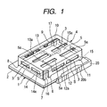
- Fig. 1 is a perspective view illustrating an antenna-integrated module according to a first embodiment of the invention.
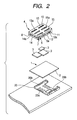
- Fig. 2 is an exploded perspective view illustrating a module and a connector shown in Fig. 1 .
- the antenna-integrated module shown in Figs. 1 and 2 includes a rectangular circuit board 1 of which the upper surface is provided with a wiring pattern of a high frequency circuit and of which the entire lower surface is provided with a ground conductive layer 2, circuit elements 3 such as a chip element or an IC which are mounted on the upper surface of the circuit board 1 so as to be connected to the wiring pattern, and a sheet-metal covering antenna element 4 which is mounted on the circuit board 1 so as to cover the circuit elements 3.
- the circuit board 1 is electrically and mechanically connected to a main board 30 with a connector 20 interposed therebetween.
- the connector 20 includes a plurality of connection terminals 20a disposed on the flat plate portion thereof and a pair of guide pieces 20b that are formed in the side walls erected from both ends of the flat plate portions.
- the circuit board 1 is regulated in the transverse direction thereof by both the side walls of the connector 20 and is also interposed in the plate-thickness direction thereof by the guide pieces 20b.
- the covering antenna element 4 includes a top plate 5 which is a rectangular flat metal plate for covering the circuit elements 3 and serves as a radiation conductor, a power feeding leg piece 6 which extends from the periphery of the top plate 5 to the circuit board 1, short-circuited leg pieces 7 and 8, support leg pieces 9 to 11, and side plates 12 to 15 which extend from the periphery (four sides) of the top plate 5 to the circuit board 1 at positions excluding the pieces 6 to 11.
- the power feeding leg piece 6 is connected to the wiring pattern and the short-circuited leg pieces 7 and 8 are connected to the ground conductive layer 2.
- the support leg pieces 9 to 11 are fixed on the circuit board as so to be 1 electrically opened.
- slit-like opening portions 5a spaced from the periphery of the top plate 5 are formed at 6 positions of the top plate 5.
- Slit-like openings 12a to 15a spaced from the periphery are formed at tow positions of each of the side plates 12 to 15.
- the side plate 12 along one long side of the top plate 5 is a bent piece of which one end in the longitudinal direction is adjoined with the power feeding leg piece 6 and the other end is adjoined with the support leg piece 11.
- the openings 12a extending along the long side of the top plate 5 are formed at two positions in line and a short-circuited leg piece 7 is formed at a position adjacent through the power feeding leg piece 6 and a notched portion 16.
- the side plate 13 along the other long side of the top plate 5 is a bent piece of which one end in the longitudinal direction is adjoined with the power feeding leg piece 8 and the other end is adjoined to the support leg piece 9.
- the openings 13a extending along the long side of the top plate 5 are formed at two positions in line and the support leg piece 10 is formed at a position adjacent the support leg piece 9 with a notched portion 17 interposed therebetween.
- the openings 14a extending along the short side are formed in line at two positions.
- the openings 15a extending along the short side are formed in line at two positions.
- the width size (slit width) of the slit-like openings 12a to 15a formed in the side plate 12 to 15 is configured to be 1 mm or less.
- gaps S are interposed in the ends (lower end portions) of the side plates 12 to 15 so as to be opposed to the circuit board 1 and the size of the opposed gaps is 1 mm or less.
- the pieces 6 to 11 of the covering antenna element 4 will be described in detail.
- the lower portion of the power feeding leg piece 6 is connected to a feeding line of the wiring pattern and a predetermined high frequency signal is configured to be supplied to a feeding point (the upper end of the bent portion of the power feeding leg piece 6) of the top plate 5 through the power feeding leg piece 6.
- the short-circuited leg pieces 7 and 8 are connected to the ground conductive layer 2 through a through-hole of the circuit board 1. All the support leg pieces 9 to 11 are connected to an electrically isolated soldering land of the circuit board 1. Electrostatic capacitance is loaded between the soldering land and the ground conductive layer 2.
- the covering antenna element 4 is stably mounted on the circuit board 1 by soldering the pieces 6 to 11 to land to the corresponding soldering land and the top plate 5 is opposite the circuit board 1 at a predetermined interval.
- the short-circuited leg piece 7 and 8 and the support leg pieces 10 and 11 are formed in four corners of the covering antenna element 4.
- the support leg piece 9 of which the shape is the same as that of the power feeding leg piece 6 is formed at a point-symmetrical position in which the support leg piece 9 is point-symmetrical to the power feeding leg piece 6. Accordingly, even through both ends in the longitudinal direction is reversed, a symmetrical structure of which the outer appearance is not different can be designed.
- the sheet-metal covering antenna element 4 which covers the circuit elements 3 is connected to the ground conductive layer 2. Therefore, the covering antenna element 4 can serve as a shield case.
- the rectangular top plate 5 of the covering antenna element 4 one end portion thereof in the longitudinal direction is provided with the short-circuited leg pieces 7 and 8 and the other end portion is electrically opened and the top plate 5 is excited by the feeding operation from the power feeding leg piece 6. Accordingly, the top plate 5 can serve as a radiation conductor of an inverted F-type sheet-metal antenna.
- the covering antenna element 4 that covers the major part of the high frequency circuit not only serves as the shield cover, but also serves as an antenna element of the inverted F-type antenna. Accordingly, it is possible to decrease the size thereof and achieve low cost, compared with a structure in which a special antenna element and a shield case are disposed in line in plan view. Moreover, the covering antenna element 4 is designed so that the support leg pieces 9 to 11 are electrically opened, that is, the electrostatic capacitance is loaded on portions which become an electric field region at the feeding time. Accordingly, it is possible to further decrease the size of the module.
- the plurality of openings 5a and the plurality of openings 12a to 15a are formed in the top plate 5 of the covering antenna element 4 and the side plates 12 to 15, respectively, and moreover air can be smoothly circulated through the openings 5a and 12a to 15a. Accordingly, in a reflow process, heat can be delivered to the region of the circuit board 1 covered with the covering antenna element 4, and thus a reflow soldering of the circuit elements 3 mounted on the circuit substrate 1 and a reflow soldering of the covering antenna element 4 can be performed together. That is, since the reflow process does not need repeatedly, it is possible to manufacture the antenna-integrated module.
- the side plates 12 to 15 extend from the periphery of the top plate 5 to the circuit board 1 and the distance (gap S) between the end of each of the side plates 12 to 15 and the circuit board 1 opposed to each other is configured to be 1 mm or less. Accordingly, it is difficult to inserting a soldering iron or the like into the space covered with the covering antenna element 4 from the side. Moreover, since the width of the slit-like openings 5a and 12a to 15a are configured to be 1 mm or less, it is difficult to inserting the soldering iron or the like into the openings 5a and 12a to 15a. As a result, it is difficult to arbitrarily alternate the major elements of the high frequency circuit of the antenna-integrated module.
- the shape of the sheet-metal covering antenna element 4 is simple, it is easy to manufacture the antenna-integrated module according to the embodiment of the invention. Moreover, the covering antenna element 4 has a point-symmetrical structure. Accordingly, even thought both ends of the covering antenna element 4 in the longitudinal direction are reversed, the outer appearance is not different. For this reason, in a manufacturing process of mounting the covering antenna element 4 on the circuit board 1, it is not necessary to check the direction of the covering antenna element 4, thereby improving the working efficiency.
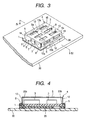
- Fig. 3 is a perspective view illustrating an antenna-integrated module according to a second embodiment of the invention.
- Fig. 4 is a sectional view illustrating the antenna-integrated module taken along the line IV-IV line shown in Fig. 3 .
- the same reference numerals are given to the same elements corresponding to those in Figs. 1 and 2 .
- the second embodiment of the invention is different from the first embodiment described above in that a circuit board 1 of a top plate 5 has a squire with the substantially same width and a power feeding leg piece 6, short-circuited leg pieces 7 and 8, support leg pieces 9 to 11 extending from the top plate 5 are formed at different positions.
- a side plate 14 along one short side of the top plate 5 is a bent piece of which one end portion in the transverse direction thereof is adjoined with the power feeding leg piece 6, a center portion is adjoined with the short-circuited leg piece 7, and the other end is adjoined with the short-circuited leg piece 8.
- a side plate 15 along the other short side of the top plate 5 is a bent piece of which one end portion, a center portion, and the other end portion are adjoined with the support leg pieces 9, 10, and 11, respectively.
- openings 12a extending along the long side are formed in line at two positions.
- openings 13a extending along the other long side are formed in line at two positions.
- the front ends of the side plates 12 to 15 are opposite the circuit board 1 with gaps S interposed therebetween.
- the gaps S are formed from end to end in the longitudinal direction thereof.
- the circuit board 1 is interested below both guide pieces 20b of a connector 20 so that the circuit board 1 is electrically and mechanically connected to a main board 30 through the connector 20. At this time, the circuit board 1 is fixed so as not to be detached from the connector 20 by both the guide pieces 20b. As shown in Fig. 4 , these guide pieces 20b are positioned in the gaps S formed between the side plate 12 and the circuit board 1 and between the side plate 13 and the circuit board 1.
- the guide pieces 20b pass through the gaps S which are formed below the side plates 12 and 13 and extend along the insertion direction of the circuit board 1. Accordingly, it is possible to avoid contact between the guide pieces 20b and the side plates 12 and 13 by the gaps S. Therefore, since the top plate 5 of the covering antenna element 4 can be expanded so as to be the same as the width size of the circuit board 1, a limited region of the circuit board 1 can be effectively used as an element-mounted region. Moreover, the broad region of the top plate 5 can be used as an attachment surface of a label (not shown).
- the opening 5a of the top plate 5 extends along the longitudinal direction.
- the opening 5a may extend along the transverse direction.
- the opening 5a or the openings 12a to 15a may be shaped in a small hole instead of the slit shape. In this case, it is possible to avoid the repetition reflow process by punching various small holes.
Landscapes
- Engineering & Computer Science (AREA)
- Computer Networks & Wireless Communication (AREA)
- Details Of Aerials (AREA)
- Waveguide Aerials (AREA)
Applications Claiming Priority (1)
| Application Number | Priority Date | Filing Date | Title |
|---|---|---|---|
| JP2006335856A JP2007259412A (ja) | 2006-02-22 | 2006-12-13 | アンテナ一体型モジュール |
Publications (1)
| Publication Number | Publication Date |
|---|---|
| EP1933416A1 true EP1933416A1 (fr) | 2008-06-18 |
Family
ID=39247967
Family Applications (1)
| Application Number | Title | Priority Date | Filing Date |
|---|---|---|---|
| EP07023678A Withdrawn EP1933416A1 (fr) | 2006-12-13 | 2007-12-06 | Module d'antenne intégrée |
Country Status (4)
| Country | Link |
|---|---|
| US (1) | US20080143608A1 (fr) |
| EP (1) | EP1933416A1 (fr) |
| CN (1) | CN101202375A (fr) |
| TW (1) | TW200832810A (fr) |
Cited By (5)
| Publication number | Priority date | Publication date | Assignee | Title |
|---|---|---|---|---|
| EP2469645A1 (fr) * | 2010-12-22 | 2012-06-27 | Laird Technologies AB | Arrangement d'antenne pour dispositif de communication radio portable doté d'un boîtier métallique |
| FR3009443A1 (fr) * | 2013-08-05 | 2015-02-06 | Insight Sip | Dispositif d'emission et/ou de reception de signaux radiofrequences |
| EP2913892A1 (fr) * | 2014-02-27 | 2015-09-02 | Alcatel Lucent | Antenne, réseau d'antennes multiples et procédé permettant de rayonner un signal radioélectrique |
| EP3370305A4 (fr) * | 2015-10-26 | 2018-09-26 | Alps Electric Co., Ltd. | Dispositif d'antenne |
| CN110943287A (zh) * | 2019-11-18 | 2020-03-31 | 深圳迈睿智能科技有限公司 | 一种微波探测模块及其制造方法 |
Families Citing this family (8)
| Publication number | Priority date | Publication date | Assignee | Title |
|---|---|---|---|---|
| CN202917625U (zh) * | 2012-10-26 | 2013-05-01 | 中怡(苏州)科技有限公司 | 具有天线及屏蔽罩一体成型的通讯装置 |
| CN104064861B (zh) * | 2014-07-01 | 2016-05-04 | 深圳市华信微通信技术有限公司 | 一种单极性高增益微带振子 |
| EP3286925B1 (fr) * | 2015-04-20 | 2022-12-07 | InterDigital Madison Patent Holdings, SAS | Montage d'antenne dans un dispositif électronique |
| CN105281010A (zh) * | 2015-09-23 | 2016-01-27 | 深圳市信维通信股份有限公司 | 一种集成摄像头的天线结构 |
| EP3526856B1 (fr) | 2016-10-12 | 2021-07-21 | Carrier Corporation | Antenne à feuille métallique inversée et trou traversant |
| EP3370303B1 (fr) * | 2016-10-21 | 2021-12-08 | KYOCERA Corporation | Substrat pour étiquettes , étiquette rfid et système rfid |
| GB2567812A (en) * | 2017-10-19 | 2019-05-01 | Raspberry Pi Trading Ltd | Radio module |
| KR102617519B1 (ko) * | 2021-04-16 | 2023-12-27 | 주식회사 아모텍 | 안테나 기능을 갖는 쉴드 캔 |
Citations (12)
| Publication number | Priority date | Publication date | Assignee | Title |
|---|---|---|---|---|
| JPH0575286A (ja) * | 1991-09-13 | 1993-03-26 | Matsushita Electric Ind Co Ltd | プリント回路の製造方法 |
| EP0621653A2 (fr) * | 1993-04-23 | 1994-10-26 | Murata Manufacturing Co., Ltd. | Unité d'antenne montable en surface |
| JPH07170087A (ja) * | 1993-12-16 | 1995-07-04 | Matsushita Electric Ind Co Ltd | シールド構成方法 |
| US5442521A (en) * | 1991-09-19 | 1995-08-15 | Nokia Mobile Phones Ltd. | Circuit board assembly |
| WO2001024311A1 (fr) * | 1999-09-27 | 2001-04-05 | Allgon Ab | Dispositif d'antennes conçu pour etre connecte a une piece d'appareil electrique |
| EP1137099A2 (fr) * | 2000-03-16 | 2001-09-26 | Nokia Mobile Phones Ltd. | Connecteur d'antenne |
| JP2002232221A (ja) | 2001-01-30 | 2002-08-16 | Alps Electric Co Ltd | 送受信ユニット |
| EP1308824A2 (fr) * | 2001-10-31 | 2003-05-07 | Kabushiki Kaisha Toshiba | Dispositif de communication sans fil et ordinateur portable correspondant |
| JP2003188620A (ja) * | 2001-12-19 | 2003-07-04 | Murata Mfg Co Ltd | モジュール一体型アンテナ |
| JP2005005866A (ja) | 2003-06-10 | 2005-01-06 | Alps Electric Co Ltd | アンテナ一体型モジュール |
| US20050104785A1 (en) * | 2003-11-18 | 2005-05-19 | Dell Products L.P. | Information handling system including passive RF tuning carrier for wireless modules |
| EP1826867A1 (fr) * | 2006-02-22 | 2007-08-29 | Alps Electric Co., Ltd. | Module d'antenne intégrée |
-
2007
- 2007-11-21 US US11/944,278 patent/US20080143608A1/en not_active Abandoned
- 2007-12-06 EP EP07023678A patent/EP1933416A1/fr not_active Withdrawn
- 2007-12-12 TW TW096147476A patent/TW200832810A/zh unknown
- 2007-12-12 CN CNA2007101865831A patent/CN101202375A/zh active Pending
Patent Citations (12)
| Publication number | Priority date | Publication date | Assignee | Title |
|---|---|---|---|---|
| JPH0575286A (ja) * | 1991-09-13 | 1993-03-26 | Matsushita Electric Ind Co Ltd | プリント回路の製造方法 |
| US5442521A (en) * | 1991-09-19 | 1995-08-15 | Nokia Mobile Phones Ltd. | Circuit board assembly |
| EP0621653A2 (fr) * | 1993-04-23 | 1994-10-26 | Murata Manufacturing Co., Ltd. | Unité d'antenne montable en surface |
| JPH07170087A (ja) * | 1993-12-16 | 1995-07-04 | Matsushita Electric Ind Co Ltd | シールド構成方法 |
| WO2001024311A1 (fr) * | 1999-09-27 | 2001-04-05 | Allgon Ab | Dispositif d'antennes conçu pour etre connecte a une piece d'appareil electrique |
| EP1137099A2 (fr) * | 2000-03-16 | 2001-09-26 | Nokia Mobile Phones Ltd. | Connecteur d'antenne |
| JP2002232221A (ja) | 2001-01-30 | 2002-08-16 | Alps Electric Co Ltd | 送受信ユニット |
| EP1308824A2 (fr) * | 2001-10-31 | 2003-05-07 | Kabushiki Kaisha Toshiba | Dispositif de communication sans fil et ordinateur portable correspondant |
| JP2003188620A (ja) * | 2001-12-19 | 2003-07-04 | Murata Mfg Co Ltd | モジュール一体型アンテナ |
| JP2005005866A (ja) | 2003-06-10 | 2005-01-06 | Alps Electric Co Ltd | アンテナ一体型モジュール |
| US20050104785A1 (en) * | 2003-11-18 | 2005-05-19 | Dell Products L.P. | Information handling system including passive RF tuning carrier for wireless modules |
| EP1826867A1 (fr) * | 2006-02-22 | 2007-08-29 | Alps Electric Co., Ltd. | Module d'antenne intégrée |
Cited By (9)
| Publication number | Priority date | Publication date | Assignee | Title |
|---|---|---|---|---|
| EP2469645A1 (fr) * | 2010-12-22 | 2012-06-27 | Laird Technologies AB | Arrangement d'antenne pour dispositif de communication radio portable doté d'un boîtier métallique |
| FR3009443A1 (fr) * | 2013-08-05 | 2015-02-06 | Insight Sip | Dispositif d'emission et/ou de reception de signaux radiofrequences |
| WO2015018745A1 (fr) * | 2013-08-05 | 2015-02-12 | Insight Sip | Dispositif d'émission et/ou de réception de signaux radiofréquences |
| JP2016529821A (ja) * | 2013-08-05 | 2016-09-23 | インサイト・シップ | 無線周波数信号を送受信するための装置 |
| US10483632B2 (en) | 2013-08-05 | 2019-11-19 | Insight Sip | Device for transmitting and/or receiving radiofrequency signals |
| EP2913892A1 (fr) * | 2014-02-27 | 2015-09-02 | Alcatel Lucent | Antenne, réseau d'antennes multiples et procédé permettant de rayonner un signal radioélectrique |
| EP3370305A4 (fr) * | 2015-10-26 | 2018-09-26 | Alps Electric Co., Ltd. | Dispositif d'antenne |
| US10411355B2 (en) | 2015-10-26 | 2019-09-10 | Alps Alpine Co., Ltd. | Antenna device |
| CN110943287A (zh) * | 2019-11-18 | 2020-03-31 | 深圳迈睿智能科技有限公司 | 一种微波探测模块及其制造方法 |
Also Published As
| Publication number | Publication date |
|---|---|
| CN101202375A (zh) | 2008-06-18 |
| TW200832810A (en) | 2008-08-01 |
| US20080143608A1 (en) | 2008-06-19 |
Similar Documents
| Publication | Publication Date | Title |
|---|---|---|
| EP1933416A1 (fr) | Module d'antenne intégrée | |
| US6958732B2 (en) | Small-sized and high-gained antenna-integrated module | |
| AU700176B2 (en) | Shield assembly and method of shielding suitable for use in a communication device | |
| JP4217596B2 (ja) | アンテナ一体型モジュール | |
| EP1821368A1 (fr) | Connecteur entre substrats et dispositif de carte de circuit l'utilisant entre des substrats | |
| JP2005166295A (ja) | カードコネクタ組立体 | |
| CN111988910A (zh) | 电子部件的实装构造及电子部件的实装方法 | |
| JP4070689B2 (ja) | 無線通信ユニット | |
| JP2007259412A (ja) | アンテナ一体型モジュール | |
| EP1826867A1 (fr) | Module d'antenne intégrée | |
| KR20050052342A (ko) | 카드 커넥터 조립체 | |
| JP2004064353A (ja) | アンテナ用部品、アンテナ装置、および、通信機器 | |
| US20070015379A1 (en) | Electronic component assembly | |
| US7247053B2 (en) | High-frequency apparatus having high performance and capable of preventing entry of interfering wave into terminal | |
| US6906603B2 (en) | High-frequency module for commonality of circuit board | |
| JP4665698B2 (ja) | アンテナ装置 | |
| US20090303151A1 (en) | Low profile gps antenna assembly | |
| JP2004319384A (ja) | 電子回路ユニット | |
| JP2007281581A (ja) | ダイバーシティアンテナ装置 | |
| US20030103341A1 (en) | Shielding structure for resonant circuit | |
| JP4160948B2 (ja) | アンテナ装置 | |
| JP2007235850A (ja) | アンテナ一体型モジュール | |
| Kim et al. | A Low EMI Board-to-board Connector Design for 5G mmWave and High-speed Signaling | |
| JP3096064U (ja) | カードリーダーの接地装置 | |
| JP2003283235A (ja) | 誘電体アンテナ |
Legal Events
| Date | Code | Title | Description |
|---|---|---|---|
| PUAI | Public reference made under article 153(3) epc to a published international application that has entered the european phase |
Free format text: ORIGINAL CODE: 0009012 |
|
| AK | Designated contracting states |
Kind code of ref document: A1 Designated state(s): AT BE BG CH CY CZ DE DK EE ES FI FR GB GR HU IE IS IT LI LT LU LV MC MT NL PL PT RO SE SI SK TR |
|
| AX | Request for extension of the european patent |
Extension state: AL BA HR MK RS |
|
| AKX | Designation fees paid | ||
| STAA | Information on the status of an ep patent application or granted ep patent |
Free format text: STATUS: THE APPLICATION IS DEEMED TO BE WITHDRAWN |
|
| 18D | Application deemed to be withdrawn |
Effective date: 20081219 |