EP1930769A2 - Flüssigkristallanzeigetafel und Herstellungsverfahren davon - Google Patents
Flüssigkristallanzeigetafel und Herstellungsverfahren davon Download PDFInfo
- Publication number
- EP1930769A2 EP1930769A2 EP07023448A EP07023448A EP1930769A2 EP 1930769 A2 EP1930769 A2 EP 1930769A2 EP 07023448 A EP07023448 A EP 07023448A EP 07023448 A EP07023448 A EP 07023448A EP 1930769 A2 EP1930769 A2 EP 1930769A2
- Authority
- EP
- European Patent Office
- Prior art keywords
- liquid crystal
- alignment
- alignment layer
- layer
- sioc
- Prior art date
- Legal status (The legal status is an assumption and is not a legal conclusion. Google has not performed a legal analysis and makes no representation as to the accuracy of the status listed.)
- Withdrawn
Links
Images




Classifications
-
- G—PHYSICS
- G02—OPTICS
- G02F—OPTICAL DEVICES OR ARRANGEMENTS FOR THE CONTROL OF LIGHT BY MODIFICATION OF THE OPTICAL PROPERTIES OF THE MEDIA OF THE ELEMENTS INVOLVED THEREIN; NON-LINEAR OPTICS; FREQUENCY-CHANGING OF LIGHT; OPTICAL LOGIC ELEMENTS; OPTICAL ANALOGUE/DIGITAL CONVERTERS
- G02F1/00—Devices or arrangements for the control of the intensity, colour, phase, polarisation or direction of light arriving from an independent light source, e.g. switching, gating or modulating; Non-linear optics
- G02F1/01—Devices or arrangements for the control of the intensity, colour, phase, polarisation or direction of light arriving from an independent light source, e.g. switching, gating or modulating; Non-linear optics for the control of the intensity, phase, polarisation or colour
- G02F1/13—Devices or arrangements for the control of the intensity, colour, phase, polarisation or direction of light arriving from an independent light source, e.g. switching, gating or modulating; Non-linear optics for the control of the intensity, phase, polarisation or colour based on liquid crystals, e.g. single liquid crystal display cells
- G02F1/133—Constructional arrangements; Operation of liquid crystal cells; Circuit arrangements
- G02F1/1333—Constructional arrangements; Manufacturing methods
- G02F1/1337—Surface-induced orientation of the liquid crystal molecules, e.g. by alignment layers
- G02F1/133734—Surface-induced orientation of the liquid crystal molecules, e.g. by alignment layers by obliquely evaporated films, e.g. Si or SiO2 films
-
- G—PHYSICS
- G02—OPTICS
- G02F—OPTICAL DEVICES OR ARRANGEMENTS FOR THE CONTROL OF LIGHT BY MODIFICATION OF THE OPTICAL PROPERTIES OF THE MEDIA OF THE ELEMENTS INVOLVED THEREIN; NON-LINEAR OPTICS; FREQUENCY-CHANGING OF LIGHT; OPTICAL LOGIC ELEMENTS; OPTICAL ANALOGUE/DIGITAL CONVERTERS
- G02F1/00—Devices or arrangements for the control of the intensity, colour, phase, polarisation or direction of light arriving from an independent light source, e.g. switching, gating or modulating; Non-linear optics
- G02F1/01—Devices or arrangements for the control of the intensity, colour, phase, polarisation or direction of light arriving from an independent light source, e.g. switching, gating or modulating; Non-linear optics for the control of the intensity, phase, polarisation or colour
- G02F1/13—Devices or arrangements for the control of the intensity, colour, phase, polarisation or direction of light arriving from an independent light source, e.g. switching, gating or modulating; Non-linear optics for the control of the intensity, phase, polarisation or colour based on liquid crystals, e.g. single liquid crystal display cells
-
- G—PHYSICS
- G02—OPTICS
- G02F—OPTICAL DEVICES OR ARRANGEMENTS FOR THE CONTROL OF LIGHT BY MODIFICATION OF THE OPTICAL PROPERTIES OF THE MEDIA OF THE ELEMENTS INVOLVED THEREIN; NON-LINEAR OPTICS; FREQUENCY-CHANGING OF LIGHT; OPTICAL LOGIC ELEMENTS; OPTICAL ANALOGUE/DIGITAL CONVERTERS
- G02F1/00—Devices or arrangements for the control of the intensity, colour, phase, polarisation or direction of light arriving from an independent light source, e.g. switching, gating or modulating; Non-linear optics
- G02F1/01—Devices or arrangements for the control of the intensity, colour, phase, polarisation or direction of light arriving from an independent light source, e.g. switching, gating or modulating; Non-linear optics for the control of the intensity, phase, polarisation or colour
- G02F1/13—Devices or arrangements for the control of the intensity, colour, phase, polarisation or direction of light arriving from an independent light source, e.g. switching, gating or modulating; Non-linear optics for the control of the intensity, phase, polarisation or colour based on liquid crystals, e.g. single liquid crystal display cells
- G02F1/133—Constructional arrangements; Operation of liquid crystal cells; Circuit arrangements
- G02F1/1333—Constructional arrangements; Manufacturing methods
- G02F1/1337—Surface-induced orientation of the liquid crystal molecules, e.g. by alignment layers
-
- G—PHYSICS
- G02—OPTICS
- G02F—OPTICAL DEVICES OR ARRANGEMENTS FOR THE CONTROL OF LIGHT BY MODIFICATION OF THE OPTICAL PROPERTIES OF THE MEDIA OF THE ELEMENTS INVOLVED THEREIN; NON-LINEAR OPTICS; FREQUENCY-CHANGING OF LIGHT; OPTICAL LOGIC ELEMENTS; OPTICAL ANALOGUE/DIGITAL CONVERTERS
- G02F1/00—Devices or arrangements for the control of the intensity, colour, phase, polarisation or direction of light arriving from an independent light source, e.g. switching, gating or modulating; Non-linear optics
- G02F1/01—Devices or arrangements for the control of the intensity, colour, phase, polarisation or direction of light arriving from an independent light source, e.g. switching, gating or modulating; Non-linear optics for the control of the intensity, phase, polarisation or colour
- G02F1/13—Devices or arrangements for the control of the intensity, colour, phase, polarisation or direction of light arriving from an independent light source, e.g. switching, gating or modulating; Non-linear optics for the control of the intensity, phase, polarisation or colour based on liquid crystals, e.g. single liquid crystal display cells
- G02F1/133—Constructional arrangements; Operation of liquid crystal cells; Circuit arrangements
- G02F1/1333—Constructional arrangements; Manufacturing methods
- G02F1/1337—Surface-induced orientation of the liquid crystal molecules, e.g. by alignment layers
- G02F1/13378—Surface-induced orientation of the liquid crystal molecules, e.g. by alignment layers by treatment of the surface, e.g. embossing, rubbing or light irradiation
-
- C—CHEMISTRY; METALLURGY
- C09—DYES; PAINTS; POLISHES; NATURAL RESINS; ADHESIVES; COMPOSITIONS NOT OTHERWISE PROVIDED FOR; APPLICATIONS OF MATERIALS NOT OTHERWISE PROVIDED FOR
- C09K—MATERIALS FOR MISCELLANEOUS APPLICATIONS, NOT PROVIDED FOR ELSEWHERE
- C09K2323/00—Functional layers of liquid crystal optical display excluding electroactive liquid crystal layer characterised by chemical composition
- C09K2323/02—Alignment layer characterised by chemical composition
-
- C—CHEMISTRY; METALLURGY
- C09—DYES; PAINTS; POLISHES; NATURAL RESINS; ADHESIVES; COMPOSITIONS NOT OTHERWISE PROVIDED FOR; APPLICATIONS OF MATERIALS NOT OTHERWISE PROVIDED FOR
- C09K—MATERIALS FOR MISCELLANEOUS APPLICATIONS, NOT PROVIDED FOR ELSEWHERE
- C09K2323/00—Functional layers of liquid crystal optical display excluding electroactive liquid crystal layer characterised by chemical composition
- C09K2323/02—Alignment layer characterised by chemical composition
- C09K2323/021—Inorganic, e.g. glass or silicon oxide
-
- C—CHEMISTRY; METALLURGY
- C09—DYES; PAINTS; POLISHES; NATURAL RESINS; ADHESIVES; COMPOSITIONS NOT OTHERWISE PROVIDED FOR; APPLICATIONS OF MATERIALS NOT OTHERWISE PROVIDED FOR
- C09K—MATERIALS FOR MISCELLANEOUS APPLICATIONS, NOT PROVIDED FOR ELSEWHERE
- C09K2323/00—Functional layers of liquid crystal optical display excluding electroactive liquid crystal layer characterised by chemical composition
- C09K2323/02—Alignment layer characterised by chemical composition
- C09K2323/023—Organic silicon compound, e.g. organosilicon
-
- G—PHYSICS
- G02—OPTICS
- G02F—OPTICAL DEVICES OR ARRANGEMENTS FOR THE CONTROL OF LIGHT BY MODIFICATION OF THE OPTICAL PROPERTIES OF THE MEDIA OF THE ELEMENTS INVOLVED THEREIN; NON-LINEAR OPTICS; FREQUENCY-CHANGING OF LIGHT; OPTICAL LOGIC ELEMENTS; OPTICAL ANALOGUE/DIGITAL CONVERTERS
- G02F1/00—Devices or arrangements for the control of the intensity, colour, phase, polarisation or direction of light arriving from an independent light source, e.g. switching, gating or modulating; Non-linear optics
- G02F1/01—Devices or arrangements for the control of the intensity, colour, phase, polarisation or direction of light arriving from an independent light source, e.g. switching, gating or modulating; Non-linear optics for the control of the intensity, phase, polarisation or colour
- G02F1/13—Devices or arrangements for the control of the intensity, colour, phase, polarisation or direction of light arriving from an independent light source, e.g. switching, gating or modulating; Non-linear optics for the control of the intensity, phase, polarisation or colour based on liquid crystals, e.g. single liquid crystal display cells
- G02F1/133—Constructional arrangements; Operation of liquid crystal cells; Circuit arrangements
- G02F1/1333—Constructional arrangements; Manufacturing methods
- G02F1/1337—Surface-induced orientation of the liquid crystal molecules, e.g. by alignment layers
- G02F1/133742—Surface-induced orientation of the liquid crystal molecules, e.g. by alignment layers for homeotropic alignment
-
- G—PHYSICS
- G02—OPTICS
- G02F—OPTICAL DEVICES OR ARRANGEMENTS FOR THE CONTROL OF LIGHT BY MODIFICATION OF THE OPTICAL PROPERTIES OF THE MEDIA OF THE ELEMENTS INVOLVED THEREIN; NON-LINEAR OPTICS; FREQUENCY-CHANGING OF LIGHT; OPTICAL LOGIC ELEMENTS; OPTICAL ANALOGUE/DIGITAL CONVERTERS
- G02F1/00—Devices or arrangements for the control of the intensity, colour, phase, polarisation or direction of light arriving from an independent light source, e.g. switching, gating or modulating; Non-linear optics
- G02F1/01—Devices or arrangements for the control of the intensity, colour, phase, polarisation or direction of light arriving from an independent light source, e.g. switching, gating or modulating; Non-linear optics for the control of the intensity, phase, polarisation or colour
- G02F1/13—Devices or arrangements for the control of the intensity, colour, phase, polarisation or direction of light arriving from an independent light source, e.g. switching, gating or modulating; Non-linear optics for the control of the intensity, phase, polarisation or colour based on liquid crystals, e.g. single liquid crystal display cells
- G02F1/133—Constructional arrangements; Operation of liquid crystal cells; Circuit arrangements
- G02F1/1333—Constructional arrangements; Manufacturing methods
- G02F1/1337—Surface-induced orientation of the liquid crystal molecules, e.g. by alignment layers
- G02F1/133746—Surface-induced orientation of the liquid crystal molecules, e.g. by alignment layers for high pretilt angles, i.e. higher than 15 degrees
Definitions
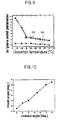
- the present invention provides an LCD panel and a manufacturing method thereof wherein the LCD display panel includes a SiOC alignment layer that has advantageous properties that are insensitive to the temperature of deposition process over a wide range of deposition temperatures. Further, the alignment direction of the SiOC alignment layer can be changed by ion beam bombardment.
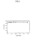
- an alignment direction of the liquid crystal layer has a pretilt angle in a range from about 85° to about 90°, the pretilt angle being set by the SiOC.
- the alignment layer is deposited in the temperature range of about 30°C to about 400°C.
- the incident angle is between about 20° and about 90°.
- a vertical alignment (“VA") mode i.e., a wide viewing angle technique in accordance with the present invention
- the liquid crystal molecules having negative permittivity anisotropy are vertically aligned and perpendicularly driven by an electric field, thus adjusting the light transmittance.
- the VA mode becomes a normally black mode since light transmittance is shut by a polarizer perpendicular to the alignment direction of the liquid crystal molecules when a voltage is not applied.
- the VA mode light is transmitted by a polarizer parallel to the alignment direction of the liquid crystal molecules rotated at a predetermined angle by an applied voltage.
- the liquid crystal 155 is vertically aligned by the vertical alignment layers 150 and 160 of SiOC, thereby preventing the light leakage.
- the multi-domain VA mode e.g., the PVA mode forms the multi-domain in a manner that a slit is provided on the common and pixel electrodes of the upper and lower substrates, and the liquid crystal molecules are symmetrically driven based on the slit using a fringe field generated by the slit.
- FIG. 6 shows the transmittance characteristic of the LCD panel in which voltages are applied to establish a voltage difference between the common and pixel electrodes 142 and 164, thus causing the liquid crystal molecules 155 to be rotated at a predetermined angle to transmit light.
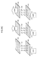
- the pretilt alignment direction of a liquid crystal layer may be defined by using an ion beam system to treat the alignment layers formed on the upper and lower substrates.
- an LCD panel including alignment layers formed of silicon oxycarbide (SiOC) in accordance with the present invention the transmittance of the LCD panel is improved, and thus the display quality is improved.
Landscapes
- Physics & Mathematics (AREA)
- Nonlinear Science (AREA)
- Chemical & Material Sciences (AREA)
- Crystallography & Structural Chemistry (AREA)
- General Physics & Mathematics (AREA)
- Optics & Photonics (AREA)
- Spectroscopy & Molecular Physics (AREA)
- Mathematical Physics (AREA)
- Liquid Crystal (AREA)
Applications Claiming Priority (1)
| Application Number | Priority Date | Filing Date | Title |
|---|---|---|---|
| KR1020060122073A KR101350908B1 (ko) | 2006-12-05 | 2006-12-05 | 액정 표시 패널 및 그 제조 방법 |
Publications (2)
| Publication Number | Publication Date |
|---|---|
| EP1930769A2 true EP1930769A2 (de) | 2008-06-11 |
| EP1930769A3 EP1930769A3 (de) | 2009-09-30 |
Family
ID=38969913
Family Applications (1)
| Application Number | Title | Priority Date | Filing Date |
|---|---|---|---|
| EP07023448A Withdrawn EP1930769A3 (de) | 2006-12-05 | 2007-12-04 | Flüssigkristallanzeigetafel und Herstellungsverfahren davon |
Country Status (6)
| Country | Link |
|---|---|
| US (1) | US7800724B2 (de) |
| EP (1) | EP1930769A3 (de) |
| JP (1) | JP2008146062A (de) |
| KR (1) | KR101350908B1 (de) |
| CN (1) | CN101206350A (de) |
| TW (1) | TW200903114A (de) |
Families Citing this family (10)
| Publication number | Priority date | Publication date | Assignee | Title |
|---|---|---|---|---|
| JP2010145734A (ja) * | 2008-12-18 | 2010-07-01 | Canon Inc | 線順次駆動型ディスプレイ |
| JP5906063B2 (ja) * | 2011-11-21 | 2016-04-20 | 株式会社ジャパンディスプレイ | 液晶表示装置およびその製造方法 |
| KR101953593B1 (ko) * | 2011-11-25 | 2019-03-05 | 엘지디스플레이 주식회사 | 액정표시장치 및 그의 제조방법 |
| KR20140091100A (ko) * | 2012-12-26 | 2014-07-21 | 삼성디스플레이 주식회사 | 곡면 액정 표시 장치 |
| US20150255029A1 (en) * | 2014-03-07 | 2015-09-10 | Semiconductor Energy Laboratory Co., Ltd. | Display device, display module including the display device, and electronic device including the display device or the display module |
| JP2017116819A (ja) * | 2015-12-25 | 2017-06-29 | 株式会社ジャパンディスプレイ | 液晶表示装置 |
| CN105785658B (zh) * | 2016-05-13 | 2018-03-30 | 深圳市华星光电技术有限公司 | 液晶面板结构及制作方法 |
| KR102401523B1 (ko) * | 2016-07-29 | 2022-05-24 | 다이니폰 인사츠 가부시키가이샤 | 조광 필름, 조광 부재, 차량, 조광 필름의 급전 방법 |
| JP7279392B2 (ja) * | 2019-02-14 | 2023-05-23 | 日本ゼオン株式会社 | 積層体 |
| CN119380672B (zh) * | 2024-11-27 | 2025-12-05 | 长城汽车股份有限公司 | 消除显示屏拖影的方法、装置以及可读存储介质 |
Family Cites Families (13)
| Publication number | Priority date | Publication date | Assignee | Title |
|---|---|---|---|---|
| JPS62115425A (ja) * | 1985-11-15 | 1987-05-27 | Ricoh Co Ltd | 液晶配向膜 |
| US6426786B1 (en) * | 1999-06-01 | 2002-07-30 | International Business Machines Corporation | Method of homeotropic alignment or tilted homeotropic alignment of liquid crystals by single oblique evaporation of oxides and liquid crystal display device formed thereby |
| US6665033B2 (en) * | 2000-11-30 | 2003-12-16 | International Business Machines Corporation | Method for forming alignment layer by ion beam surface modification |
| US6660341B2 (en) * | 2001-06-07 | 2003-12-09 | International Business Machines Corporation | Tilted vertical alignment of liquid crystals employing inorganic thin film composition and ion beam treatment |
| US6890850B2 (en) * | 2001-12-14 | 2005-05-10 | Applied Materials, Inc. | Method of depositing dielectric materials in damascene applications |
| JP2005274641A (ja) | 2004-03-23 | 2005-10-06 | Sony Corp | 液晶パネルの製造方法および液晶パネル |
| JP4878779B2 (ja) * | 2004-06-10 | 2012-02-15 | 富士フイルム株式会社 | 膜形成用組成物、絶縁膜及び電子デバイス |
| KR20060066284A (ko) | 2004-12-13 | 2006-06-16 | 삼성에스디아이 주식회사 | 액정 표시 장치 |
| KR20060093070A (ko) | 2005-02-18 | 2006-08-23 | 세이코 엡슨 가부시키가이샤 | 무기 배향막의 형성 방법, 무기 배향막, 전자 장치용 기판,액정 패널 및 전자기기 |
| US20070224365A1 (en) * | 2006-03-22 | 2007-09-27 | Callegari Alessandro C | High pretilt homogeneous alignment and tilted vertical alignment by surface modification of thin films with nitrogen ion beam |
| US20080018841A1 (en) * | 2006-07-24 | 2008-01-24 | Samsung Electronics Co., Ltd. | Methods and apparatus for forming LCD alignment films |
| JP2008090279A (ja) * | 2006-09-04 | 2008-04-17 | Epson Imaging Devices Corp | 液晶表示装置及び電子機器 |
| JP2008129482A (ja) * | 2006-11-24 | 2008-06-05 | Nec Lcd Technologies Ltd | 液晶表示装置及びその製造方法 |
-
2006
- 2006-12-05 KR KR1020060122073A patent/KR101350908B1/ko not_active Expired - Fee Related
-
2007
- 2007-12-04 JP JP2007314004A patent/JP2008146062A/ja active Pending
- 2007-12-04 EP EP07023448A patent/EP1930769A3/de not_active Withdrawn
- 2007-12-04 US US11/999,380 patent/US7800724B2/en active Active
- 2007-12-05 CN CNA2007103068881A patent/CN101206350A/zh active Pending
- 2007-12-05 TW TW096146355A patent/TW200903114A/zh unknown
Also Published As
| Publication number | Publication date |
|---|---|
| EP1930769A3 (de) | 2009-09-30 |
| CN101206350A (zh) | 2008-06-25 |
| KR101350908B1 (ko) | 2014-01-16 |
| US20080158492A1 (en) | 2008-07-03 |
| KR20080051284A (ko) | 2008-06-11 |
| TW200903114A (en) | 2009-01-16 |
| JP2008146062A (ja) | 2008-06-26 |
| US7800724B2 (en) | 2010-09-21 |
Similar Documents
| Publication | Publication Date | Title |
|---|---|---|
| US7800724B2 (en) | Liquid crystal display panel and manufacturing method thereof | |
| US8045112B2 (en) | Display device and method of manufacturing the same | |
| US8040481B2 (en) | In-plane switching mode liquid crystal display device having first and second common electrode connection lines and first and second pixel electrode connection linesbeing formed on the same layer | |
| JP3723336B2 (ja) | 液晶表示装置 | |
| US7834970B2 (en) | Multi-domain liquid crystal display device and method for manufacturing the same | |
| US20090040441A1 (en) | Liquid crystal display and manufacturing method thereof | |
| US8300181B2 (en) | Method of fabricating liquid crystal display and liquid crystal display obtained by the method | |
| US8154695B2 (en) | Liquid crystal display and method of fabricating the same | |
| JP2006072324A (ja) | 横電界方式の液晶表示装置及びその製造方法 | |
| US8654284B2 (en) | Display substrate, method of manufacturing the same and display device having the same | |
| US20060255337A1 (en) | Multi-domain member for a display device | |
| JP4469331B2 (ja) | 液晶表示装置の配向膜形成方法 | |
| JP2001201749A (ja) | マルチドメイン液晶表示素子 | |
| KR100244730B1 (ko) | 액정표시소자 제조방법 | |
| JP2009122707A (ja) | 液晶表示装置 | |
| KR100617027B1 (ko) | 액정표시소자 제조방법 | |
| KR100484949B1 (ko) | 배향막을 형성하기 위한 이온빔 조사 장치 | |
| KR100235381B1 (ko) | 액정표시장치 및 제조방법 | |
| US20070110922A1 (en) | Alignment Film, Method of Forming the Same, and Liquid Crystal Display Including the Same | |
| KR101244528B1 (ko) | 횡전계 방식 액정 표시 장치 및 그 제조 방법 | |
| KR20180047551A (ko) | 액정표시장치 | |
| KR101057851B1 (ko) | 액정 표시 장치의 제조 방법 | |
| JP4290150B2 (ja) | 液晶表示装置 | |
| KR20070052183A (ko) | 배향막 형성 방법, 그에 의해 형성된 배향막 및 배향막을포함하는 액정 표시 장치 | |
| KR20080062406A (ko) | 액정표시장치 |
Legal Events
| Date | Code | Title | Description |
|---|---|---|---|
| PUAI | Public reference made under article 153(3) epc to a published international application that has entered the european phase |
Free format text: ORIGINAL CODE: 0009012 |
|
| AK | Designated contracting states |
Kind code of ref document: A2 Designated state(s): AT BE BG CH CY CZ DE DK EE ES FI FR GB GR HU IE IS IT LI LT LU LV MC MT NL PL PT RO SE SI SK TR |
|
| AX | Request for extension of the european patent |
Extension state: AL BA HR MK RS |
|
| RIN1 | Information on inventor provided before grant (corrected) |
Inventor name: PARK, JEUN-HUN Inventor name: SON, PHIL-KOOK Inventor name: YOON, TEE-HOON Inventor name: KIM, JAE-CHANG Inventor name: LEE, HAE-KEUN Inventor name: JEON, BAEK-KYUN Inventor name: KIM, JANG-SUB Inventor name: RHO, SOON-JOON |
|
| PUAL | Search report despatched |
Free format text: ORIGINAL CODE: 0009013 |
|
| AK | Designated contracting states |
Kind code of ref document: A3 Designated state(s): AT BE BG CH CY CZ DE DK EE ES FI FR GB GR HU IE IS IT LI LT LU LV MC MT NL PL PT RO SE SI SK TR |
|
| AX | Request for extension of the european patent |
Extension state: AL BA HR MK RS |
|
| 17P | Request for examination filed |
Effective date: 20100323 |
|
| 17Q | First examination report despatched |
Effective date: 20100423 |
|
| AKX | Designation fees paid |
Designated state(s): CH FR GB LI |
|
| STAA | Information on the status of an ep patent application or granted ep patent |
Free format text: STATUS: THE APPLICATION HAS BEEN WITHDRAWN |
|
| REG | Reference to a national code |
Ref country code: DE Ref legal event code: 8566 |
|
| 18W | Application withdrawn |
Effective date: 20100621 |