EP1929552B1 - Élément semi-conducteur optoélectronique doté d'une couche d'étalement du courant - Google Patents
Élément semi-conducteur optoélectronique doté d'une couche d'étalement du courant Download PDFInfo
- Publication number
- EP1929552B1 EP1929552B1 EP06849368A EP06849368A EP1929552B1 EP 1929552 B1 EP1929552 B1 EP 1929552B1 EP 06849368 A EP06849368 A EP 06849368A EP 06849368 A EP06849368 A EP 06849368A EP 1929552 B1 EP1929552 B1 EP 1929552B1
- Authority
- EP
- European Patent Office
- Prior art keywords
- current spreading
- layer
- metal
- spreading layer
- semiconductor body
- Prior art date
- Legal status (The legal status is an assumption and is not a legal conclusion. Google has not performed a legal analysis and makes no representation as to the accuracy of the status listed.)
- Active
Links
Images

Classifications
-
- H—ELECTRICITY
- H10—SEMICONDUCTOR DEVICES; ELECTRIC SOLID-STATE DEVICES NOT OTHERWISE PROVIDED FOR
- H10F—INORGANIC SEMICONDUCTOR DEVICES SENSITIVE TO INFRARED RADIATION, LIGHT, ELECTROMAGNETIC RADIATION OF SHORTER WAVELENGTH OR CORPUSCULAR RADIATION
- H10F77/00—Constructional details of devices covered by this subclass
- H10F77/20—Electrodes
- H10F77/244—Electrodes made of transparent conductive layers, e.g. transparent conductive oxide [TCO] layers
-
- H—ELECTRICITY
- H10—SEMICONDUCTOR DEVICES; ELECTRIC SOLID-STATE DEVICES NOT OTHERWISE PROVIDED FOR
- H10F—INORGANIC SEMICONDUCTOR DEVICES SENSITIVE TO INFRARED RADIATION, LIGHT, ELECTROMAGNETIC RADIATION OF SHORTER WAVELENGTH OR CORPUSCULAR RADIATION
- H10F30/00—Individual radiation-sensitive semiconductor devices in which radiation controls the flow of current through the devices, e.g. photodetectors
- H10F30/20—Individual radiation-sensitive semiconductor devices in which radiation controls the flow of current through the devices, e.g. photodetectors the devices having potential barriers, e.g. phototransistors
- H10F30/21—Individual radiation-sensitive semiconductor devices in which radiation controls the flow of current through the devices, e.g. photodetectors the devices having potential barriers, e.g. phototransistors the devices being sensitive to infrared, visible or ultraviolet radiation
- H10F30/22—Individual radiation-sensitive semiconductor devices in which radiation controls the flow of current through the devices, e.g. photodetectors the devices having potential barriers, e.g. phototransistors the devices being sensitive to infrared, visible or ultraviolet radiation the devices having only one potential barrier, e.g. photodiodes
- H10F30/221—Individual radiation-sensitive semiconductor devices in which radiation controls the flow of current through the devices, e.g. photodetectors the devices having potential barriers, e.g. phototransistors the devices being sensitive to infrared, visible or ultraviolet radiation the devices having only one potential barrier, e.g. photodiodes the potential barrier being a PN homojunction
-
- H—ELECTRICITY
- H10—SEMICONDUCTOR DEVICES; ELECTRIC SOLID-STATE DEVICES NOT OTHERWISE PROVIDED FOR
- H10F—INORGANIC SEMICONDUCTOR DEVICES SENSITIVE TO INFRARED RADIATION, LIGHT, ELECTROMAGNETIC RADIATION OF SHORTER WAVELENGTH OR CORPUSCULAR RADIATION
- H10F71/00—Manufacture or treatment of devices covered by this subclass
- H10F71/138—Manufacture of transparent electrodes, e.g. transparent conductive oxides [TCO] or indium tin oxide [ITO] electrodes
-
- H—ELECTRICITY
- H10—SEMICONDUCTOR DEVICES; ELECTRIC SOLID-STATE DEVICES NOT OTHERWISE PROVIDED FOR
- H10H—INORGANIC LIGHT-EMITTING SEMICONDUCTOR DEVICES HAVING POTENTIAL BARRIERS
- H10H20/00—Individual inorganic light-emitting semiconductor devices having potential barriers, e.g. light-emitting diodes [LED]
- H10H20/80—Constructional details
- H10H20/83—Electrodes
- H10H20/832—Electrodes characterised by their material
- H10H20/833—Transparent materials
-
- H—ELECTRICITY
- H01—ELECTRIC ELEMENTS
- H01S—DEVICES USING THE PROCESS OF LIGHT AMPLIFICATION BY STIMULATED EMISSION OF RADIATION [LASER] TO AMPLIFY OR GENERATE LIGHT; DEVICES USING STIMULATED EMISSION OF ELECTROMAGNETIC RADIATION IN WAVE RANGES OTHER THAN OPTICAL
- H01S5/00—Semiconductor lasers
- H01S5/04—Processes or apparatus for excitation, e.g. pumping, e.g. by electron beams
- H01S5/042—Electrical excitation ; Circuits therefor
- H01S5/0421—Electrical excitation ; Circuits therefor characterised by the semiconducting contacting layers
-
- H—ELECTRICITY
- H10—SEMICONDUCTOR DEVICES; ELECTRIC SOLID-STATE DEVICES NOT OTHERWISE PROVIDED FOR
- H10H—INORGANIC LIGHT-EMITTING SEMICONDUCTOR DEVICES HAVING POTENTIAL BARRIERS
- H10H20/00—Individual inorganic light-emitting semiconductor devices having potential barriers, e.g. light-emitting diodes [LED]
- H10H20/01—Manufacture or treatment
-
- H—ELECTRICITY
- H10—SEMICONDUCTOR DEVICES; ELECTRIC SOLID-STATE DEVICES NOT OTHERWISE PROVIDED FOR
- H10W—GENERIC PACKAGES, INTERCONNECTIONS, CONNECTORS OR OTHER CONSTRUCTIONAL DETAILS OF DEVICES COVERED BY CLASS H10
- H10W72/00—Interconnections or connectors in packages
- H10W72/50—Bond wires
- H10W72/531—Shapes of wire connectors
- H10W72/536—Shapes of wire connectors the connected ends being ball-shaped
-
- Y—GENERAL TAGGING OF NEW TECHNOLOGICAL DEVELOPMENTS; GENERAL TAGGING OF CROSS-SECTIONAL TECHNOLOGIES SPANNING OVER SEVERAL SECTIONS OF THE IPC; TECHNICAL SUBJECTS COVERED BY FORMER USPC CROSS-REFERENCE ART COLLECTIONS [XRACs] AND DIGESTS
- Y02—TECHNOLOGIES OR APPLICATIONS FOR MITIGATION OR ADAPTATION AGAINST CLIMATE CHANGE
- Y02E—REDUCTION OF GREENHOUSE GAS [GHG] EMISSIONS, RELATED TO ENERGY GENERATION, TRANSMISSION OR DISTRIBUTION
- Y02E10/00—Energy generation through renewable energy sources
- Y02E10/50—Photovoltaic [PV] energy
Definitions
- An optoelectronic semiconductor component is specified.
- An object to be solved is to specify an optoelectronic semiconductor component which has an electrically and mechanically particularly stable contacting.
- a further object is to specify methods for producing such an optoelectronic semiconductor component.
- the optoelectronic semiconductor component comprises a semiconductor body.
- the semiconductor body contains, for example, a semiconductor layer sequence which is suitable for generating radiation or for converting electromagnetic radiation into electrical charges.
- the semiconductor body is an epitaxially grown semiconductor body.
- the semiconductor body is at least placed in places a current spreading layer.
- the current spreading layer is preferably characterized by a particularly good electrical transverse conductivity. That is, the current spreading layer is capable of distributing a current impressed in a limited area of the current spreading layer into as large an area as possible.
- the current spreading layer is particularly well suited to conduct the electric current impressed into it in directions parallel to a major surface of the current spreading layer.
- the current spreading layer is additionally permeable to at least some of the electromagnetic radiation generated in the optoelectronic semiconductor chip or received by the optoelectronic semiconductor chip.
- the transmissivity of the current spreading layer is preferably at least 90 percent for electromagnetic radiation in the visible spectral range.
- the current spreading layer contains a metal which forms a transparent, electrically conductive metal oxide in the current spreading layer. That is, the current spreading layer contains, at least in places, a transparent, electrically conductive metal oxide.
- the current spreading layer preferably comprises a material from the group of so-called transparent conductive oxides (TCOs).
- TCOs transparent conductive oxides
- the metal oxide of the current spreading layer it is possible for the metal oxide of the current spreading layer to be n-doped or p-doped with another material, for example a metal or a semiconductor.
- the concentration of the metal forming an oxide in the current spreading layer decreases from the side of the current spreading layer facing the semiconductor body to the side of the current spreading layer facing away from the semiconductor body. That is, on the side of the current spreading layer facing the semiconductor body, the metal concentration is highest.
- the concentration of the metal can be up to 100 percent there. That is, there, the current spreading layer may include an area made of the metal.
- the concentration of the metal in the current spreading layer then decreases.
- the concentration of oxygen increases accordingly.
- the metal oxide of the current spreading layer may have a stoichiometric composition in places on its side facing away from the semiconductor body.
- an optoelectronic semiconductor component with a semiconductor body has a current spreading layer, which is applied at least in places to the semiconductor body.
- the current spreading layer includes a metal that forms a transparent, electrically conductive metal oxide in the current spreading layer, and the concentration of the metal decreases from the side of the current spreading layer facing the semiconductor body to the side facing away from the semiconductor body.
- the optoelectronic semiconductor component makes use, inter alia, of the knowledge that one is possible high metal concentration at the interface between the semiconductor body and the current spreading layer enables a particularly good ohmic contact between the semiconductor body and the current spreading layer. Furthermore, it has been found that due to the increased metal concentration on the semiconductor body, the current spreading layer adheres particularly well to the semiconductor body and the risk of detachment of the current spreading layer from the semiconductor body is thereby reduced. Furthermore, the current spreading layer can be produced in a particularly simple manner if the metal-rich region of the current spreading layer, that is to say the region of the current spreading layer in the vicinity of the semiconductor body, comprises the metal which forms the metal oxide in the current spreading layer.
- the metal concentration in the current spreading layer decreases continuously.
- the metal concentration does not change abruptly in such a manner that only unoxidized metal is contained in a region of the current spreading layer and only metal oxide is contained in an adjacent region of the current spreading layer. Rather, the transition from a metal-rich to a metal-poorer region of the current spreading layer is fluid.
- the current spreading layer comprises in places a metal oxide of stoichiometric composition. That is, there are areas in the current spreading layer in which a metal oxide is in a stoichiometric composition. For example, the current spreading layer near the Semiconductor body on a high metal concentration. With increasing distance from the semiconductor body, the metal concentration can then decrease in such a way that, on the side of the current spreading layer facing away from the semiconductor body, there is in places a metal oxide of stoichiometric composition. In other words, there are regions of the current spreading layer in which metal atoms present there are each bound to at least one oxygen atom.
- the current spreading layer comprises oxides of at least one of the following metals or metal alloys: indium, tin; Indium tin, zinc, cadmium, titanium. Possible oxides in the current spreading layer are then given, for example, by the following oxides: ZnO, SnO 2 , In 2 O 3 , Zn 2 SnO 4 , CdSnO 3 , ZnSnO 3 , MgIn 2 O 4 , GaInO 3 , Zn 2 In 2 O 5 , In 4 Sn 3 O 12 or mixtures.
- the metal oxides are doped n- or p-type.
- the current spreading layer is applied to a radiation passage area of the optoelectronic semiconductor component.
- the radiation passage area is a surface of the optoelectronic semiconductor component through which electromagnetic radiation enters the semiconductor body or emerges from the semiconductor body through the electromagnetic radiation.
- the optoelectronic semiconductor component can be, for example, one of the following components: photodiode chip, LED chip, laser diode chip.
- an optoelectronic component is specified.
- an optoelectronic semiconductor component according to at least one of the embodiments described above can be produced by means of the method.
- first of all a layer comprising a metal is applied at least in places to the surface of a semiconductor body.
- the metal layer is applied to the radiation passage area of the semiconductor body.
- the thickness of the metal layer is preferably between at least 0.2 and at most 3.0 nanometers.
- the layer thickness of the metal layer is particularly preferably between 0.3 and 2.0 nanometers.
- the layer thickness is preferably selected to be so thin that it is permeable to a large part of the electromagnetic radiation emitted by the optoelectronic semiconductor component during operation or to be received by the optoelectronic semiconductor component.
- the metal layer preferably contains or consists of one of the above-mentioned metals. That is, it contains or consists of at least one of the following metals: indium, tin, indium tin, zinc, cadmium, titanium. Furthermore, the metal layer may also contain or consist of metal alloys such as gold zinc (AuZn).
- a layer which comprises an oxide of a metal of the metal layer is applied to the metal layer.
- the metal oxide layer contains or consists of at least one of the following metal oxides: ZnO, SnO 2 , In 2 O 3 , Zn 2 SnO 4 , ZnSnO 3 , CdSnO 3 , MgIn 2 O 4 , GaInO 3 , Zn 2 In 2 O 5 , In 4 Sn 3 O 12 .
- the layer sequence of metal layer and metal oxide layer applied to the semiconductor body is subsequently thermally treated.
- the applied layer sequence is heated, for example, to temperatures between 200 and 600 degrees Celsius, preferably at temperatures between 300 and 500 degrees Celsius. This temperature range proves to be particularly advantageous for producing a particularly well electrically conductive Stormierweitungstik.
- the layer sequence can be heated, for example, in a kiln with 0 to 20% partial pressure oxygen, particularly preferably 2 to 10% partial pressure oxygen. This range of partial pressure proves to be particularly advantageous for producing a particularly well electrically conductive Stormaufweitungs Mrs.
- an RTA (rapid thermal annealing) technique can also be used. Furthermore, it is possible that the layer sequence is heated under N 2 , N 2 / Ar or N 2 / H 2 atmosphere.
- the layer sequence is preferably heated for times between one and five minutes. This range of the duration of the heating of the layer sequence proves to be particularly advantageous for producing a particularly well electrically conductive Stormierweitungs Mrs.
- At least one layer comprising a metal is applied to a semiconductor body.
- a layer comprising an oxide of the metal is applied to the metal layer.
- the applied layer sequence of metal and metal oxide layer is thermally treated.
- the described method makes use of the knowledge that through the thermal treatment a thorough reaction of the metal and the metal oxide layer is made possible. As a result, a course of the metal concentration can be generated in the current spreading layer.
- the concentration of the metal in the current spreading layer decreases in the direction away from the semiconductor body.
- a desired profile of the metal concentration in the current spreading layer can be generated.
- the method described here exploits, inter alia, the idea that a mechanically and electrically particularly stable ohmic contact between the semiconductor body and the current spreading layer can be produced by means of the thin metal layer at the interface between the current spreading layer and the semiconductor body. Furthermore, the metal layer for Dotierverêtung the current spreading layer serve at the interface between the semiconductor body and current spreading layer.
- a metal is applied to the semiconductor body to produce the current spreading layer, wherein the deposited metal is oxidized at an increasing rate in the course of the application or coating process.
- the oxygen flux is increased, so that in the course of the coating an ever increasing proportion of the applied metal is oxidized.
- a current spreading layer can be produced in which the metal concentration decreases with increasing distance from the semiconductor body and the oxygen concentration increases.
- the coating can be done by means of reactive sputtering of the metal, whereby the oxygen flow is increased in the course of the coating process.
- the current spreading layer by means of a PVD (short for physical vapor deposition) or CVD (short for chemical vapor deposition) method is applied.
- the oxygen concentration is preferably enriched during the deposition process.
- the oxygen concentration in the current spreading layer is adjusted in such a way that a highly conductive metal oxide layer results.
- the process makes use of the idea that the oxygen supply can be used
- Metal concentration in the growing current spreading layer can be controlled. In this way, a predeterminable profile of the metal concentration in the current spreading layer can be set.
- the oxygen flux is continuously increased during the coating process.
- FIGS. 1A, 1B and 1C show schematic sectional views for explaining an embodiment of the method described here for producing an optoelectronic semiconductor device.
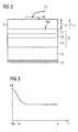
- FIG. 2 shows a schematic sectional view of an embodiment of the optoelectronic semiconductor device described here.
- FIG. 3 schematically shows the course of the metal concentration in the current spreading layer of an embodiment of the optoelectronic semiconductor device described here.
- FIGS. 1A to 1C show schematic sectional views for explaining a first embodiment of the method for producing an optoelectronic semiconductor device.
- Figure 1A shows a schematic sectional view of a semiconductor body 10.
- the semiconductor body 10 includes a cladding layer 11, which may be doped p-type, for example.
- the cladding layer 11 may be doped, for example, with a p-type dopant.
- the semiconductor body 10 further comprises an active zone 12 which comprises, for example, an epitaxial layer sequence suitable for generating radiation.
- the epitaxial layer sequence may include, for example, a pn junction, a quantum well structure, or a multiple quantum well structure.
- quantum well structure also encompasses any structure in which charge carriers undergo quantization of their energy states by confinement.
- quantum well structure does not include information about the dimensionality of the quantization. It thus includes u.a. Quantum wells, quantum wires and quantum dots and any combination of these structures.
- the epitaxial layer sequence is preferably based on a phosphide, arsenide or nitride compound semiconductor material.
- phosphide compound semiconductors means that a component or part of a component designated in this way preferably comprises Al n Ga m In 1-nm P, where 0 ⁇ n ⁇ 1, 0 ⁇ m ⁇ 1 and n + m ⁇ 1.
- This material does not necessarily have to have a mathematically exact composition according to the above formula. Rather, it may include one or more dopants as well as additional ingredients that do not substantially alter the physical properties of the material.
- the above formula includes only the essential constituents of the crystal lattice (Al, Ga, In, P), even though these may be partially replaced by small amounts of other substances.
- a component or part of a component designated in this way preferably comprises Al n Ga m In 1-nm As, where 0 ⁇ n ⁇ 1, 0 ⁇ m ⁇ 1 and n + m ⁇ 1.
- This material does not necessarily have to have a mathematically exact composition according to the above formula. Rather, it may include one or more dopants as well as additional ingredients that do not substantially alter the physical properties of the material.
- the above formula contains only the essential components of the crystal lattice (Al, Ga, In, As), even though these may be partially replaced by small amounts of other substances.
- nitride compound semiconductor based means that the active epitaxial layer sequence or at least one layer thereof is a nitride III / V compound semiconductor material, preferably Al n Ga m In 1-nm N, where 0 ⁇ n ⁇ 1, 0 ⁇ m ⁇ 1 and n + m ⁇ 1.
- this material does not necessarily have to have a mathematically exact composition according to the above formula. Rather, it may comprise one or more dopants as well as additional constituents which do not substantially alter the characteristic physical properties of the Al n Ga m In 1-nm n material.
- the above formula contains only the essential constituents of the crystal lattice (Al, Ga, In, N), even if these may be partially replaced by small amounts of other substances.
- the semiconductor body 10 preferably comprises a cladding layer 13, which may be n-type.
- the cladding layer 13 is doped with an n-type dopant for this purpose.
- the semiconductor body 10 is preferably applied to a carrier 14.
- the carrier 14 may be a growth substrate for the layers of the semiconductor body 10.
- the semiconductor body 10 is then epitaxially grown on the carrier 14.
- the carrier 14 may be a carrier element to which the semiconductor body 10 has been subsequently applied, that is to say after completion of the growth of the semiconductor body 10.
- the optoelectronic semiconductor chip is a so-called thin-film chip.
- the carrier 14 of the semiconductor device may then be relatively freely selected as compared to a growth substrate.
- a carrier 14 is selected which is particularly well adapted to the radiation-generating epitaxial layer sequence 12 with regard to its temperature expansion coefficient.
- the carrier 14 may include a material that especially good heat is conductive. In this way, the heat generated during operation is particularly efficiently dissipated to another carrier, such as a printed circuit board.
- a basic principle of a thin-film LED chip is, for example, in the document I. Schnitzer et al., Appl. Phys. Lett. 63 (16), 18 October 1993, pages 2174 to 2176 described.
- the semiconductor body 10 further preferably has a radiation passage area 10a through which a majority of the optoelectronic semiconductor chip, for example emitted electromagnetic radiation is coupled out. Particularly preferably, the entire radiation emitted by the optoelectronic semiconductor component emerges through the radiation passage area 10a.
- the radiation passage area 10a is formed, for example, by a part of the surface of the semiconductor body 10.
- the radiation passage area 10a is provided by a main surface of the semiconductor body 10, which is arranged, for example, parallel to an epitaxial layer sequence 12 of the semiconductor body 10, which is suitable for generating electromagnetic radiation.
- the semiconductor body 10 may include further layers not shown.
- the semiconductor body 10 may include buffer layers for matching lattice differences between one or more of the described layers.
- a contact layer 15 is preferably applied on the surface of the carrier 14 facing away from the semiconductor body.
- the contact layer 15 is, for example, a contact metallization. Via the contact metallization, the optoelectronic semiconductor component can be contacted on the n-side, for example.
- a thin metal layer 1 is first applied to the radiation passage area 10a of the semiconductor body 10.
- the metal layer 1 may be, for example, by PVD or CVD coating techniques at a temperature of preferably be applied between 150 degrees Celsius and 350 degrees Celsius.
- the following coating methods are preferred: sputtering, magnetron sputtering, DC sputtering, electron beam evaporation.
- the thickness d1 of the metal layer 1 is preferably between 0.2 and 3.0 nanometers, particularly preferably between 0.3 and 2.0 nanometers.
- the thickness d1 is selected to be so thin that the metal layer 1 is transparent to a large part of the electromagnetic radiation generated, for example, during operation of the optoelectronic semiconductor component.
- the metal layer 1 contains one of the following metals or consists of one of the following metals: indium, tin, indium tin, zinc, cadmium, titanium. In the described embodiment of the method, the metal layer 1 consists of zinc or a gold zinc alloy.
- a metal oxide layer 2 is applied to the metal layer 1.
- the metal oxide layer 2 may be applied, for example, by PVD or CVD coating techniques.
- the following coating methods are preferred: sputtering, magnetron sputtering, DC sputtering, electron beam evaporation.
- the metal oxide layer 2 preferably has a thickness of at least 50 nanometers, particularly preferably of at least 200 nanometers. It contains a transparent, electrically conductive metal oxide (TCO).
- TCO transparent, electrically conductive metal oxide
- the metal oxide layer contains an oxide of at least one metal of the metal layer 1 or consists of this oxide.
- the metal oxide layer 2 contains or consists of one of the following metal oxides: ZnO, SnO 2 , In 2 O 3 , Zn 2 SnO 4 , CdSnO 3 , ZnSnO 3 , MgIn 2 O 4 , GaInO 3 , Zn 2 In 2 O 5 , In 4 Sn 3 O 12 or mixtures.
- the metal oxide layer preferably contains a zinc oxide or an aluminum-doped p-type zinc oxide (ZnO: Al).
- the applied layer sequence is preferably thermally treated.
- the layer sequence is heated to temperatures between 30 degrees Celsius and 1,000 degrees Celsius, preferably between 200 degrees Celsius and 600 degrees Celsius, more preferably between 300 degrees Celsius and 500 degrees Celsius.
- the material of the metal layer 1 and the metal oxide layer 2 reacts to form a current spreading layer 3 with the thickness d.
- the layer sequence can be heated, for example, in a kiln with 0 to 20% partial pressure oxygen, particularly preferably 2 to 10% partial pressure oxygen.
- an RTA (rapid thermal annealing) technique can also be used.
- the layer sequence is heated under N 2 , N 2 / Ar or N 2 / H 2 atmosphere.
- the layer sequence is preferably heated for times between one and five minutes.
- FIG. 2 shows an optoelectronic semiconductor device, for example by means of the in conjunction with the FIGS. 1A to 1C described method is made.
- a wire connection point 16 bond pad
- electrical current can be impressed into the current spreading layer 3 via the wire connection point 16.
- the current is distributed in directions parallel to the radiation passage area 10a-that is, in the transverse direction-such that the most uniform possible distribution of the impressed current takes place over the entire radiation passage area 10a. In this way, a particularly uniform energization of the active zone 12 of the semiconductor body 10 is possible.
- the metal concentration x is particularly high and can be, for example, up to 100 percent. This is, for example, an average metal concentration x, wherein the metal concentration is averaged depending on the distance z from the radiation passage area 10a via the surface of the current expansion layer 3 parallel to the radiation passage area 10a.
- metal passes, for example, by diffusion from the metal layer 1 into the metal oxide layer 2.
- the result is a quasi-continuous course of the metal concentration x, wherein the metal concentration x decreases continuously with increasing distance from the radiation passage area 10a in the direction z. That is, the metal concentration x does not abruptly drop at the distance d 1 corresponding to the layer thickness of the original metal layer 1, but the transition between the original metal layer 1 and metal oxide layer 2 is fluid with respect to the metal concentration x.
- the steepness of the drop in the metal concentration x and the metal concentration as a function of the distance from the radiation passage area 10a can be adjusted, inter alia, by the temperature during the thermal treatment of the layers 1, 2 and by the duration of the thermal treatment.
- the profile of the metal concentration which arises in the current spreading layer 3 depends on the materials used and the desired conductivity of the current spreading layer 3.
- the course of the metal concentration x in the current spreading layer 3 can be adjusted particularly accurately by means of a second exemplary embodiment of the method for producing an optoelectronic semiconductor component.
- the metal is applied under oxygen supply, that is, for example, in an oxygen atmosphere.
- the oxygen flow during the coating process is varied.
- the oxygen flow is continuously increased during the coating process until a desired, specifiable oxygen content in the metal oxide layer 2 is reached. That is, in this method, not only a pure metal layer 1 and then a pure metal oxide layer 2 is applied first, but it is applied to a metal oxide layer in which the oxygen content is varied controlled during the coating process.
- a metal layer can be applied, in which the oxygen content is zero or approximately zero.
- a current spreading layer 3 is formed, in which the profile of the metal concentration x is adjustable as a function of the distance from the radiation passage area 10a by means of the oxygen flow.
- a ZnO layer is deposited on the semiconductor body 10 by reactively sputtering zinc from a zinc target, thereby increasing the oxygen flux during the sputtering process.
Landscapes
- Led Devices (AREA)
- Photovoltaic Devices (AREA)
Abstract
Claims (15)
- Composant semiconducteur optoélectronique qui présente- un corps semiconducteur (10) et- une couche d'élargissement du courant (3) qui est appliquée au moins par endroits sur le corps semiconducteur (10), dans lequel- la couche d'élargissement du courant (3) contient un métal (1) qui forme dans la couche d'élargissement du courant un oxyde métallique (2) électriquement conducteur transparent, et- la concentration (x) du métal (1), qui forme l'oxyde métallique (2) électriquement conducteur transparent, diminue depuis le côté de la couche d'élargissement du courant (3) faisant face au corps semiconducteur (10) vers le côté opposé au corps semiconducteur (10) à mesure que l'espacement du corps semiconducteur (10) augmente,
caractérisé en ce que- la concentration d'oxygène dans l'oxyde métallique augmente en fonction d'une diminution de la concentration du métal (1) à mesure que l'espacement du corps semiconducteur (10) augmente et- la couche d'élargissement du courant (3) se compose de l'oxyde métallique sur son côté à l'opposé du corps semiconducteur (10). - Composant semiconducteur optoélectronique selon la revendication précédente,
dans lequel la concentration de métal dans la couche d'élargissement du courant (3) diminue continuellement. - Composant semiconducteur optoélectronique selon au moins l'une des revendications précédentes,
dans lequel la couche d'élargissement du courant (3) comprend par endroits une composition stoechiométrique d'oxyde métallique. - Composant semiconducteur optoélectronique selon au moins l'une des revendications précédentes,
dans lequel la couche d'élargissement du courant (3) comprend des oxydes d'au moins l'un des métaux suivants : indium, étain, indium-étain, zinc, cadmium, titane. - Composant semiconducteur optoélectronique selon au moins l'une des revendications précédentes,
dans lequel la couche d'élargissement du courant (3) est appliquée sur une surface de traversée de rayonnement (10a) du corps semiconducteur (10). - Composant semiconducteur optoélectronique selon au moins l'une des revendications précédentes,
dans lequel le composant semiconducteur optoélectronique comprend au moins l'un des composants suivants : puce de photodiode, puce de diode électroluminescente, puce de diode laser. - Procédé de fabrication d'un composant optoélectronique selon au moins l'une des revendications précédentes, présentant les étapes suivantes :a) Application sur le corps semiconducteur (10) d'une couche contenant un métal (1),b) Application sur la couche métallique (1) d'une couche (2) contenant un oxyde du métal, etc) Traitement thermique de la séquence de couches appliquées en vue de produire la couche d'élargissement du courant (3).
- Procédé selon la revendication précédente, l'épaisseur de la couche métallique (1) dans l'étape a) étant d'au moins 0,3 nm et d'au plus 2,0 nm.
- Procédé selon au moins l'une des revendications précédentes 7 ou 8, la séquence de couches appliquées étant chauffée dans l'étape c) sous une pression partielle d'oxygène entre au moins 2 % et au plus 10 %.
- Procédé selon au moins l'une des revendications précédentes 7 à 9, la séquence de couches appliquées étant chauffée dans l'étape c) à des températures comprises entre au moins 300 degrés Celsius et au plus 500 degrés Celsius.
- Procédé selon au moins l'une des revendications précédentes 7 à 10, la séquence de couches appliquées étant chauffée dans l'étape c) pendant des durées comprises entre au moins une minute et au plus cinq minutes.
- Procédé selon au moins l'une des revendications précédentes 7 à 11, la séquence de couches appliquées étant chauffée sous une atmosphère de N2, N2/Ar ou N2/H2.
- Procédé de fabrication d'un composant semiconducteur optoélectronique selon au moins l'une des revendications 1 à 6,
un métal (1) étant appliqué sur le corps semiconducteur (10) pour produire la couche d'élargissement du courant (3) et l'oxydation étant réalisée avec une vitesse croissante au cours de l'opération d'application. - Procédé selon la revendication précédente, la couche d'élargissement du courant (3) étant formée par pulvérisation cathodique réactive du métal.
- Procédé selon la revendication 13 ou la revendication 14, la vitesse augmentant continuellement pendant l'opération d'application.
Applications Claiming Priority (2)
| Application Number | Priority Date | Filing Date | Title |
|---|---|---|---|
| DE102005046190A DE102005046190A1 (de) | 2005-09-27 | 2005-09-27 | Optoelektronisches Halbleiterbauelement mit Stromaufweitungsschicht |
| PCT/DE2006/001617 WO2007087769A2 (fr) | 2005-09-27 | 2006-09-14 | Élément semi-conducteur optoélectronique doté d'une couche d'étalement du courant |
Publications (2)
| Publication Number | Publication Date |
|---|---|
| EP1929552A2 EP1929552A2 (fr) | 2008-06-11 |
| EP1929552B1 true EP1929552B1 (fr) | 2009-11-04 |
Family
ID=37596262
Family Applications (1)
| Application Number | Title | Priority Date | Filing Date |
|---|---|---|---|
| EP06849368A Active EP1929552B1 (fr) | 2005-09-27 | 2006-09-14 | Élément semi-conducteur optoélectronique doté d'une couche d'étalement du courant |
Country Status (8)
| Country | Link |
|---|---|
| US (1) | US8501513B2 (fr) |
| EP (1) | EP1929552B1 (fr) |
| JP (1) | JP2009510738A (fr) |
| KR (1) | KR101278851B1 (fr) |
| CN (1) | CN101273468B (fr) |
| DE (2) | DE102005046190A1 (fr) |
| TW (1) | TWI312205B (fr) |
| WO (1) | WO2007087769A2 (fr) |
Families Citing this family (11)
| Publication number | Priority date | Publication date | Assignee | Title |
|---|---|---|---|---|
| DE102008052405A1 (de) * | 2008-10-21 | 2010-04-22 | Osram Opto Semiconductors Gmbh | Optoelektronisches Halbleiterbauelement |
| JP4886766B2 (ja) | 2008-12-25 | 2012-02-29 | 株式会社東芝 | 半導体発光素子 |
| DE102009054784A1 (de) * | 2009-12-16 | 2011-06-22 | Osram Gesellschaft mit beschränkter Haftung, 81543 | Halbleiterchip und Verfahren zum Herstellen eines Halbleiterchips |
| JP5957012B2 (ja) * | 2011-12-28 | 2016-07-27 | パナソニック株式会社 | 光電気素子 |
| US9391232B1 (en) * | 2014-12-19 | 2016-07-12 | Intermolecular, Inc. | Variable composition transparent conductive oxide layer and methods of forming thereof |
| CN104617181B (zh) * | 2015-01-22 | 2017-05-24 | 苏州苏纳光电有限公司 | 基于ITO电流扩展层的InGaAs雪崩红外探测器及其制备方法 |
| CN105489732B (zh) * | 2015-12-08 | 2017-12-22 | 天津三安光电有限公司 | 垂直发光二极管的制作方法 |
| DE102016106928A1 (de) * | 2016-04-14 | 2017-10-19 | Osram Opto Semiconductors Gmbh | Optoelektronischer Halbleiterchip und Verfahren zur Herstellung eines optoelektronischen Halbleiterchips |
| CN108461597A (zh) * | 2018-02-02 | 2018-08-28 | 南昌大学 | 一种发光二极管电极装置 |
| DE102019100799A1 (de) | 2019-01-14 | 2020-07-16 | Osram Opto Semiconductors Gmbh | Optoelektronisches halbleiterbauelement mit einem schichtstapel mit anisotroper leitfähigkeit und verfahren zur herstellung des optoelektronischen halbleiterbauelements |
| US12446378B2 (en) | 2022-09-29 | 2025-10-14 | Bolb Inc. | Current spreading structure for light-emitting diode |
Citations (1)
| Publication number | Priority date | Publication date | Assignee | Title |
|---|---|---|---|---|
| US5760423A (en) * | 1996-11-08 | 1998-06-02 | Kabushiki Kaisha Toshiba | Semiconductor light emitting device, electrode of the same device and method of manufacturing the same device |
Family Cites Families (19)
| Publication number | Priority date | Publication date | Assignee | Title |
|---|---|---|---|---|
| US4495514A (en) * | 1981-03-02 | 1985-01-22 | Eastman Kodak Company | Transparent electrode light emitting diode and method of manufacture |
| JPH07283167A (ja) | 1994-04-12 | 1995-10-27 | Sumitomo Chem Co Ltd | 3−5族化合物半導体用電極材料 |
| US5861636A (en) | 1995-04-11 | 1999-01-19 | Nec Corporation | Surface emitting visible light emiting diode having ring-shaped electrode |
| TW385375B (en) * | 1996-07-26 | 2000-03-21 | Asahi Glass Co Ltd | Transparent conductive film and forming method for transparent electrode |
| US6287947B1 (en) * | 1999-06-08 | 2001-09-11 | Lumileds Lighting, U.S. Llc | Method of forming transparent contacts to a p-type GaN layer |
| US6693352B1 (en) * | 2000-06-05 | 2004-02-17 | Emitronix Inc. | Contact structure for group III-V semiconductor devices and method of producing the same |
| JP2002314132A (ja) | 2001-04-11 | 2002-10-25 | Hitachi Cable Ltd | 半導体発光ダイオードおよび半導体発光ダイオード用エピタキシャルウェハ |
| JP3697609B2 (ja) | 2001-05-23 | 2005-09-21 | 日立電線株式会社 | 半導体発光素子 |
| DE10203809B4 (de) | 2002-01-31 | 2010-05-27 | Osram Opto Semiconductors Gmbh | Strahlungsemittierendes Halbleiterbauelement |
| US6777257B2 (en) | 2002-05-17 | 2004-08-17 | Shin-Etsu Handotai Co., Ltd. | Method of fabricating a light emitting device and light emitting device |
| JP4121551B2 (ja) | 2002-10-23 | 2008-07-23 | 信越半導体株式会社 | 発光素子の製造方法及び発光素子 |
| US7041529B2 (en) | 2002-10-23 | 2006-05-09 | Shin-Etsu Handotai Co., Ltd. | Light-emitting device and method of fabricating the same |
| CN100477298C (zh) * | 2003-07-04 | 2009-04-08 | 厦门市三安光电科技有限公司 | 一种发光二极管外延结构 |
| WO2005022496A2 (fr) | 2003-08-29 | 2005-03-10 | Semiconductor Energy Laboratory Co., Ltd. | Dispositif d'affichage et procede permettant de produire ce dispositif |
| JP2007504639A (ja) | 2003-08-29 | 2007-03-01 | オスラム オプト セミコンダクターズ ゲゼルシャフト ミット ベシュレンクテル ハフツング | 放射放出半導体素子 |
| DE10346606B4 (de) | 2003-08-29 | 2012-03-01 | Osram Opto Semiconductors Gmbh | Strahlungsemittierendes Halbleiterbauelement |
| KR100571818B1 (ko) * | 2003-10-08 | 2006-04-17 | 삼성전자주식회사 | 질화물계 발광소자 및 그 제조방법 |
| JP4543700B2 (ja) | 2004-02-27 | 2010-09-15 | 日亜化学工業株式会社 | 半導体発光素子 |
| JP2005150772A (ja) | 2005-02-02 | 2005-06-09 | Sharp Corp | 半導体発光素子および製造方法 |
-
2005
- 2005-09-27 DE DE102005046190A patent/DE102005046190A1/de not_active Withdrawn
-
2006
- 2006-09-14 WO PCT/DE2006/001617 patent/WO2007087769A2/fr not_active Ceased
- 2006-09-14 KR KR1020087009927A patent/KR101278851B1/ko active Active
- 2006-09-14 US US11/992,706 patent/US8501513B2/en not_active Expired - Fee Related
- 2006-09-14 CN CN2006800356471A patent/CN101273468B/zh active Active
- 2006-09-14 EP EP06849368A patent/EP1929552B1/fr active Active
- 2006-09-14 JP JP2008532584A patent/JP2009510738A/ja active Pending
- 2006-09-14 DE DE502006005304T patent/DE502006005304D1/de active Active
- 2006-09-22 TW TW095135081A patent/TWI312205B/zh active
Patent Citations (1)
| Publication number | Priority date | Publication date | Assignee | Title |
|---|---|---|---|---|
| US5760423A (en) * | 1996-11-08 | 1998-06-02 | Kabushiki Kaisha Toshiba | Semiconductor light emitting device, electrode of the same device and method of manufacturing the same device |
Also Published As
| Publication number | Publication date |
|---|---|
| WO2007087769A3 (fr) | 2007-09-20 |
| DE102005046190A1 (de) | 2007-04-05 |
| US8501513B2 (en) | 2013-08-06 |
| JP2009510738A (ja) | 2009-03-12 |
| TW200717880A (en) | 2007-05-01 |
| TWI312205B (en) | 2009-07-11 |
| KR101278851B1 (ko) | 2013-07-01 |
| EP1929552A2 (fr) | 2008-06-11 |
| US20090262773A1 (en) | 2009-10-22 |
| KR20080068675A (ko) | 2008-07-23 |
| CN101273468B (zh) | 2010-05-19 |
| DE502006005304D1 (de) | 2009-12-17 |
| WO2007087769A2 (fr) | 2007-08-09 |
| CN101273468A (zh) | 2008-09-24 |
Similar Documents
| Publication | Publication Date | Title |
|---|---|---|
| EP2193555B1 (fr) | Élément semi-conducteur optoélectronique | |
| EP2011142B1 (fr) | Procédé de fabrication d'un substrat composite | |
| DE69501511T2 (de) | Vorrichtung mit II-VI-Halbleiterverbindung und Herstellungsverfahren | |
| DE102007032555A1 (de) | Halbleiterchip und Verfahren zur Herstellung eines Halbleiterchips | |
| DE10048196A1 (de) | Verbindungshalbleiter-Bauteil und Verfahren zum Herstellen desselben | |
| DE112018000553B4 (de) | Optoelektronischer Halbleiterchip | |
| EP2519980A1 (fr) | Puce à semi-conducteurs luminescente | |
| DE10203801A1 (de) | Halbleiterbauelement und Verfahren zu dessen Herstellung | |
| EP1929552B1 (fr) | Élément semi-conducteur optoélectronique doté d'une couche d'étalement du courant | |
| EP2980864A1 (fr) | Puce semi-conductrice optoelectronique et procede de fabrication d'une structure de contact pour une telle puce | |
| EP1658643B1 (fr) | Dispositif a semi-conducteur emetteur de rayonnement | |
| EP2338182B1 (fr) | Composant optoélectronique à semi-conducteur | |
| WO2012028511A1 (fr) | Puce semi-conductrice optoélectronique et procédé de fabrication d'une puce semi-conductrice optoélectronique | |
| WO2003026029A1 (fr) | Composant a semi-conducteur emettant un rayonnement et son procede de production | |
| DE10346605A1 (de) | Strahlungemittierendes Halbleiterbauelement | |
| EP2286469B1 (fr) | Corps en semiconducteur et procede de fabrication d' un corps en semiconducteur | |
| EP1929551B1 (fr) | Puce a semi-conducteur optoelectronique | |
| WO2013045328A1 (fr) | Puce semi-conductrice optoélectronique et procédé de fabrication d'une puce semi-conductrice optoélectronique | |
| DE102004061865A1 (de) | Verfahren zur Herstellung eines Dünnfilmhalbleiterchips | |
| WO2015176873A1 (fr) | Procédé de fabrication d'une puce de semi-conducteur optoélectronique et puce de semi-conducteur optoélectronique | |
| DE69513711T2 (de) | Halbleitervorrichtung aus II-VI-Verbindung und Herstellungsverfahren | |
| WO2014019917A1 (fr) | Système de couches de contact réfléchissantes pour un composant optoélectronique et procédé pour le fabriquer | |
| DE10308322B4 (de) | Verfahren zum Herstellen eines elektrischen Kontaktbereiches auf einer Halbleiterschicht und Bauelement mit derartigem Kontaktbereich | |
| WO2013041279A1 (fr) | Puce de semi-conducteur émettant un rayonnement | |
| DE102004004780B9 (de) | Verfahren zum Herstellen eines Bauelementes mit einem elektrischen Kontaktbereich und Bauelement mit einem elektrischen Kontaktbereich |
Legal Events
| Date | Code | Title | Description |
|---|---|---|---|
| PUAI | Public reference made under article 153(3) epc to a published international application that has entered the european phase |
Free format text: ORIGINAL CODE: 0009012 |
|
| 17P | Request for examination filed |
Effective date: 20080228 |
|
| AK | Designated contracting states |
Kind code of ref document: A2 Designated state(s): DE |
|
| RBV | Designated contracting states (corrected) |
Designated state(s): DE |
|
| 17Q | First examination report despatched |
Effective date: 20080926 |
|
| GRAP | Despatch of communication of intention to grant a patent |
Free format text: ORIGINAL CODE: EPIDOSNIGR1 |
|
| RIC1 | Information provided on ipc code assigned before grant |
Ipc: H01S 5/042 20060101ALI20090325BHEP Ipc: H01L 31/0224 20060101ALI20090325BHEP Ipc: H01L 33/00 20060101AFI20090325BHEP Ipc: H01L 31/18 20060101ALN20090325BHEP Ipc: H01L 31/103 20060101ALN20090325BHEP |
|
| DAX | Request for extension of the european patent (deleted) | ||
| GRAS | Grant fee paid |
Free format text: ORIGINAL CODE: EPIDOSNIGR3 |
|
| GRAA | (expected) grant |
Free format text: ORIGINAL CODE: 0009210 |
|
| AK | Designated contracting states |
Kind code of ref document: B1 Designated state(s): DE |
|
| REF | Corresponds to: |
Ref document number: 502006005304 Country of ref document: DE Date of ref document: 20091217 Kind code of ref document: P |
|
| PLBE | No opposition filed within time limit |
Free format text: ORIGINAL CODE: 0009261 |
|
| STAA | Information on the status of an ep patent application or granted ep patent |
Free format text: STATUS: NO OPPOSITION FILED WITHIN TIME LIMIT |
|
| 26N | No opposition filed |
Effective date: 20100805 |
|
| P01 | Opt-out of the competence of the unified patent court (upc) registered |
Effective date: 20230825 |
|
| REG | Reference to a national code |
Ref country code: DE Ref legal event code: R079 Ref document number: 502006005304 Country of ref document: DE Free format text: PREVIOUS MAIN CLASS: H01L0033000000 Ipc: H10H0020000000 |
|
| PGFP | Annual fee paid to national office [announced via postgrant information from national office to epo] |
Ref country code: DE Payment date: 20250919 Year of fee payment: 20 |