EP1929552B1 - Optoelectronic semiconductor component with current spreading layer - Google Patents
Optoelectronic semiconductor component with current spreading layer Download PDFInfo
- Publication number
- EP1929552B1 EP1929552B1 EP06849368A EP06849368A EP1929552B1 EP 1929552 B1 EP1929552 B1 EP 1929552B1 EP 06849368 A EP06849368 A EP 06849368A EP 06849368 A EP06849368 A EP 06849368A EP 1929552 B1 EP1929552 B1 EP 1929552B1
- Authority
- EP
- European Patent Office
- Prior art keywords
- current spreading
- layer
- metal
- spreading layer
- semiconductor body
- Prior art date
- Legal status (The legal status is an assumption and is not a legal conclusion. Google has not performed a legal analysis and makes no representation as to the accuracy of the status listed.)
- Active
Links
Images

Classifications
-
- H—ELECTRICITY
- H10—SEMICONDUCTOR DEVICES; ELECTRIC SOLID-STATE DEVICES NOT OTHERWISE PROVIDED FOR
- H10F—INORGANIC SEMICONDUCTOR DEVICES SENSITIVE TO INFRARED RADIATION, LIGHT, ELECTROMAGNETIC RADIATION OF SHORTER WAVELENGTH OR CORPUSCULAR RADIATION
- H10F77/00—Constructional details of devices covered by this subclass
- H10F77/20—Electrodes
- H10F77/244—Electrodes made of transparent conductive layers, e.g. transparent conductive oxide [TCO] layers
-
- H—ELECTRICITY
- H10—SEMICONDUCTOR DEVICES; ELECTRIC SOLID-STATE DEVICES NOT OTHERWISE PROVIDED FOR
- H10F—INORGANIC SEMICONDUCTOR DEVICES SENSITIVE TO INFRARED RADIATION, LIGHT, ELECTROMAGNETIC RADIATION OF SHORTER WAVELENGTH OR CORPUSCULAR RADIATION
- H10F30/00—Individual radiation-sensitive semiconductor devices in which radiation controls the flow of current through the devices, e.g. photodetectors
- H10F30/20—Individual radiation-sensitive semiconductor devices in which radiation controls the flow of current through the devices, e.g. photodetectors the devices having potential barriers, e.g. phototransistors
- H10F30/21—Individual radiation-sensitive semiconductor devices in which radiation controls the flow of current through the devices, e.g. photodetectors the devices having potential barriers, e.g. phototransistors the devices being sensitive to infrared, visible or ultraviolet radiation
- H10F30/22—Individual radiation-sensitive semiconductor devices in which radiation controls the flow of current through the devices, e.g. photodetectors the devices having potential barriers, e.g. phototransistors the devices being sensitive to infrared, visible or ultraviolet radiation the devices having only one potential barrier, e.g. photodiodes
- H10F30/221—Individual radiation-sensitive semiconductor devices in which radiation controls the flow of current through the devices, e.g. photodetectors the devices having potential barriers, e.g. phototransistors the devices being sensitive to infrared, visible or ultraviolet radiation the devices having only one potential barrier, e.g. photodiodes the potential barrier being a PN homojunction
-
- H—ELECTRICITY
- H10—SEMICONDUCTOR DEVICES; ELECTRIC SOLID-STATE DEVICES NOT OTHERWISE PROVIDED FOR
- H10F—INORGANIC SEMICONDUCTOR DEVICES SENSITIVE TO INFRARED RADIATION, LIGHT, ELECTROMAGNETIC RADIATION OF SHORTER WAVELENGTH OR CORPUSCULAR RADIATION
- H10F71/00—Manufacture or treatment of devices covered by this subclass
- H10F71/138—Manufacture of transparent electrodes, e.g. transparent conductive oxides [TCO] or indium tin oxide [ITO] electrodes
-
- H—ELECTRICITY
- H10—SEMICONDUCTOR DEVICES; ELECTRIC SOLID-STATE DEVICES NOT OTHERWISE PROVIDED FOR
- H10H—INORGANIC LIGHT-EMITTING SEMICONDUCTOR DEVICES HAVING POTENTIAL BARRIERS
- H10H20/00—Individual inorganic light-emitting semiconductor devices having potential barriers, e.g. light-emitting diodes [LED]
- H10H20/80—Constructional details
- H10H20/83—Electrodes
- H10H20/832—Electrodes characterised by their material
- H10H20/833—Transparent materials
-
- H—ELECTRICITY
- H01—ELECTRIC ELEMENTS
- H01S—DEVICES USING THE PROCESS OF LIGHT AMPLIFICATION BY STIMULATED EMISSION OF RADIATION [LASER] TO AMPLIFY OR GENERATE LIGHT; DEVICES USING STIMULATED EMISSION OF ELECTROMAGNETIC RADIATION IN WAVE RANGES OTHER THAN OPTICAL
- H01S5/00—Semiconductor lasers
- H01S5/04—Processes or apparatus for excitation, e.g. pumping, e.g. by electron beams
- H01S5/042—Electrical excitation ; Circuits therefor
- H01S5/0421—Electrical excitation ; Circuits therefor characterised by the semiconducting contacting layers
-
- H—ELECTRICITY
- H10—SEMICONDUCTOR DEVICES; ELECTRIC SOLID-STATE DEVICES NOT OTHERWISE PROVIDED FOR
- H10H—INORGANIC LIGHT-EMITTING SEMICONDUCTOR DEVICES HAVING POTENTIAL BARRIERS
- H10H20/00—Individual inorganic light-emitting semiconductor devices having potential barriers, e.g. light-emitting diodes [LED]
- H10H20/01—Manufacture or treatment
-
- H—ELECTRICITY
- H10—SEMICONDUCTOR DEVICES; ELECTRIC SOLID-STATE DEVICES NOT OTHERWISE PROVIDED FOR
- H10W—GENERIC PACKAGES, INTERCONNECTIONS, CONNECTORS OR OTHER CONSTRUCTIONAL DETAILS OF DEVICES COVERED BY CLASS H10
- H10W72/00—Interconnections or connectors in packages
- H10W72/50—Bond wires
- H10W72/531—Shapes of wire connectors
- H10W72/536—Shapes of wire connectors the connected ends being ball-shaped
-
- Y—GENERAL TAGGING OF NEW TECHNOLOGICAL DEVELOPMENTS; GENERAL TAGGING OF CROSS-SECTIONAL TECHNOLOGIES SPANNING OVER SEVERAL SECTIONS OF THE IPC; TECHNICAL SUBJECTS COVERED BY FORMER USPC CROSS-REFERENCE ART COLLECTIONS [XRACs] AND DIGESTS
- Y02—TECHNOLOGIES OR APPLICATIONS FOR MITIGATION OR ADAPTATION AGAINST CLIMATE CHANGE
- Y02E—REDUCTION OF GREENHOUSE GAS [GHG] EMISSIONS, RELATED TO ENERGY GENERATION, TRANSMISSION OR DISTRIBUTION
- Y02E10/00—Energy generation through renewable energy sources
- Y02E10/50—Photovoltaic [PV] energy
Definitions
- An optoelectronic semiconductor component is specified.
- An object to be solved is to specify an optoelectronic semiconductor component which has an electrically and mechanically particularly stable contacting.
- a further object is to specify methods for producing such an optoelectronic semiconductor component.
- the optoelectronic semiconductor component comprises a semiconductor body.
- the semiconductor body contains, for example, a semiconductor layer sequence which is suitable for generating radiation or for converting electromagnetic radiation into electrical charges.
- the semiconductor body is an epitaxially grown semiconductor body.
- the semiconductor body is at least placed in places a current spreading layer.
- the current spreading layer is preferably characterized by a particularly good electrical transverse conductivity. That is, the current spreading layer is capable of distributing a current impressed in a limited area of the current spreading layer into as large an area as possible.
- the current spreading layer is particularly well suited to conduct the electric current impressed into it in directions parallel to a major surface of the current spreading layer.
- the current spreading layer is additionally permeable to at least some of the electromagnetic radiation generated in the optoelectronic semiconductor chip or received by the optoelectronic semiconductor chip.
- the transmissivity of the current spreading layer is preferably at least 90 percent for electromagnetic radiation in the visible spectral range.
- the current spreading layer contains a metal which forms a transparent, electrically conductive metal oxide in the current spreading layer. That is, the current spreading layer contains, at least in places, a transparent, electrically conductive metal oxide.
- the current spreading layer preferably comprises a material from the group of so-called transparent conductive oxides (TCOs).
- TCOs transparent conductive oxides
- the metal oxide of the current spreading layer it is possible for the metal oxide of the current spreading layer to be n-doped or p-doped with another material, for example a metal or a semiconductor.
- the concentration of the metal forming an oxide in the current spreading layer decreases from the side of the current spreading layer facing the semiconductor body to the side of the current spreading layer facing away from the semiconductor body. That is, on the side of the current spreading layer facing the semiconductor body, the metal concentration is highest.
- the concentration of the metal can be up to 100 percent there. That is, there, the current spreading layer may include an area made of the metal.
- the concentration of the metal in the current spreading layer then decreases.
- the concentration of oxygen increases accordingly.
- the metal oxide of the current spreading layer may have a stoichiometric composition in places on its side facing away from the semiconductor body.
- an optoelectronic semiconductor component with a semiconductor body has a current spreading layer, which is applied at least in places to the semiconductor body.
- the current spreading layer includes a metal that forms a transparent, electrically conductive metal oxide in the current spreading layer, and the concentration of the metal decreases from the side of the current spreading layer facing the semiconductor body to the side facing away from the semiconductor body.
- the optoelectronic semiconductor component makes use, inter alia, of the knowledge that one is possible high metal concentration at the interface between the semiconductor body and the current spreading layer enables a particularly good ohmic contact between the semiconductor body and the current spreading layer. Furthermore, it has been found that due to the increased metal concentration on the semiconductor body, the current spreading layer adheres particularly well to the semiconductor body and the risk of detachment of the current spreading layer from the semiconductor body is thereby reduced. Furthermore, the current spreading layer can be produced in a particularly simple manner if the metal-rich region of the current spreading layer, that is to say the region of the current spreading layer in the vicinity of the semiconductor body, comprises the metal which forms the metal oxide in the current spreading layer.
- the metal concentration in the current spreading layer decreases continuously.
- the metal concentration does not change abruptly in such a manner that only unoxidized metal is contained in a region of the current spreading layer and only metal oxide is contained in an adjacent region of the current spreading layer. Rather, the transition from a metal-rich to a metal-poorer region of the current spreading layer is fluid.
- the current spreading layer comprises in places a metal oxide of stoichiometric composition. That is, there are areas in the current spreading layer in which a metal oxide is in a stoichiometric composition. For example, the current spreading layer near the Semiconductor body on a high metal concentration. With increasing distance from the semiconductor body, the metal concentration can then decrease in such a way that, on the side of the current spreading layer facing away from the semiconductor body, there is in places a metal oxide of stoichiometric composition. In other words, there are regions of the current spreading layer in which metal atoms present there are each bound to at least one oxygen atom.
- the current spreading layer comprises oxides of at least one of the following metals or metal alloys: indium, tin; Indium tin, zinc, cadmium, titanium. Possible oxides in the current spreading layer are then given, for example, by the following oxides: ZnO, SnO 2 , In 2 O 3 , Zn 2 SnO 4 , CdSnO 3 , ZnSnO 3 , MgIn 2 O 4 , GaInO 3 , Zn 2 In 2 O 5 , In 4 Sn 3 O 12 or mixtures.
- the metal oxides are doped n- or p-type.
- the current spreading layer is applied to a radiation passage area of the optoelectronic semiconductor component.
- the radiation passage area is a surface of the optoelectronic semiconductor component through which electromagnetic radiation enters the semiconductor body or emerges from the semiconductor body through the electromagnetic radiation.
- the optoelectronic semiconductor component can be, for example, one of the following components: photodiode chip, LED chip, laser diode chip.
- an optoelectronic component is specified.
- an optoelectronic semiconductor component according to at least one of the embodiments described above can be produced by means of the method.
- first of all a layer comprising a metal is applied at least in places to the surface of a semiconductor body.
- the metal layer is applied to the radiation passage area of the semiconductor body.
- the thickness of the metal layer is preferably between at least 0.2 and at most 3.0 nanometers.
- the layer thickness of the metal layer is particularly preferably between 0.3 and 2.0 nanometers.
- the layer thickness is preferably selected to be so thin that it is permeable to a large part of the electromagnetic radiation emitted by the optoelectronic semiconductor component during operation or to be received by the optoelectronic semiconductor component.
- the metal layer preferably contains or consists of one of the above-mentioned metals. That is, it contains or consists of at least one of the following metals: indium, tin, indium tin, zinc, cadmium, titanium. Furthermore, the metal layer may also contain or consist of metal alloys such as gold zinc (AuZn).
- a layer which comprises an oxide of a metal of the metal layer is applied to the metal layer.
- the metal oxide layer contains or consists of at least one of the following metal oxides: ZnO, SnO 2 , In 2 O 3 , Zn 2 SnO 4 , ZnSnO 3 , CdSnO 3 , MgIn 2 O 4 , GaInO 3 , Zn 2 In 2 O 5 , In 4 Sn 3 O 12 .
- the layer sequence of metal layer and metal oxide layer applied to the semiconductor body is subsequently thermally treated.
- the applied layer sequence is heated, for example, to temperatures between 200 and 600 degrees Celsius, preferably at temperatures between 300 and 500 degrees Celsius. This temperature range proves to be particularly advantageous for producing a particularly well electrically conductive Stormierweitungstik.
- the layer sequence can be heated, for example, in a kiln with 0 to 20% partial pressure oxygen, particularly preferably 2 to 10% partial pressure oxygen. This range of partial pressure proves to be particularly advantageous for producing a particularly well electrically conductive Stormaufweitungs Mrs.
- an RTA (rapid thermal annealing) technique can also be used. Furthermore, it is possible that the layer sequence is heated under N 2 , N 2 / Ar or N 2 / H 2 atmosphere.
- the layer sequence is preferably heated for times between one and five minutes. This range of the duration of the heating of the layer sequence proves to be particularly advantageous for producing a particularly well electrically conductive Stormierweitungs Mrs.
- At least one layer comprising a metal is applied to a semiconductor body.
- a layer comprising an oxide of the metal is applied to the metal layer.
- the applied layer sequence of metal and metal oxide layer is thermally treated.
- the described method makes use of the knowledge that through the thermal treatment a thorough reaction of the metal and the metal oxide layer is made possible. As a result, a course of the metal concentration can be generated in the current spreading layer.
- the concentration of the metal in the current spreading layer decreases in the direction away from the semiconductor body.
- a desired profile of the metal concentration in the current spreading layer can be generated.
- the method described here exploits, inter alia, the idea that a mechanically and electrically particularly stable ohmic contact between the semiconductor body and the current spreading layer can be produced by means of the thin metal layer at the interface between the current spreading layer and the semiconductor body. Furthermore, the metal layer for Dotierverêtung the current spreading layer serve at the interface between the semiconductor body and current spreading layer.
- a metal is applied to the semiconductor body to produce the current spreading layer, wherein the deposited metal is oxidized at an increasing rate in the course of the application or coating process.
- the oxygen flux is increased, so that in the course of the coating an ever increasing proportion of the applied metal is oxidized.
- a current spreading layer can be produced in which the metal concentration decreases with increasing distance from the semiconductor body and the oxygen concentration increases.
- the coating can be done by means of reactive sputtering of the metal, whereby the oxygen flow is increased in the course of the coating process.
- the current spreading layer by means of a PVD (short for physical vapor deposition) or CVD (short for chemical vapor deposition) method is applied.
- the oxygen concentration is preferably enriched during the deposition process.
- the oxygen concentration in the current spreading layer is adjusted in such a way that a highly conductive metal oxide layer results.
- the process makes use of the idea that the oxygen supply can be used
- Metal concentration in the growing current spreading layer can be controlled. In this way, a predeterminable profile of the metal concentration in the current spreading layer can be set.
- the oxygen flux is continuously increased during the coating process.
- FIGS. 1A, 1B and 1C show schematic sectional views for explaining an embodiment of the method described here for producing an optoelectronic semiconductor device.
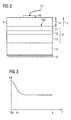
- FIG. 2 shows a schematic sectional view of an embodiment of the optoelectronic semiconductor device described here.
- FIG. 3 schematically shows the course of the metal concentration in the current spreading layer of an embodiment of the optoelectronic semiconductor device described here.
- FIGS. 1A to 1C show schematic sectional views for explaining a first embodiment of the method for producing an optoelectronic semiconductor device.
- Figure 1A shows a schematic sectional view of a semiconductor body 10.
- the semiconductor body 10 includes a cladding layer 11, which may be doped p-type, for example.
- the cladding layer 11 may be doped, for example, with a p-type dopant.
- the semiconductor body 10 further comprises an active zone 12 which comprises, for example, an epitaxial layer sequence suitable for generating radiation.
- the epitaxial layer sequence may include, for example, a pn junction, a quantum well structure, or a multiple quantum well structure.
- quantum well structure also encompasses any structure in which charge carriers undergo quantization of their energy states by confinement.
- quantum well structure does not include information about the dimensionality of the quantization. It thus includes u.a. Quantum wells, quantum wires and quantum dots and any combination of these structures.
- the epitaxial layer sequence is preferably based on a phosphide, arsenide or nitride compound semiconductor material.
- phosphide compound semiconductors means that a component or part of a component designated in this way preferably comprises Al n Ga m In 1-nm P, where 0 ⁇ n ⁇ 1, 0 ⁇ m ⁇ 1 and n + m ⁇ 1.
- This material does not necessarily have to have a mathematically exact composition according to the above formula. Rather, it may include one or more dopants as well as additional ingredients that do not substantially alter the physical properties of the material.
- the above formula includes only the essential constituents of the crystal lattice (Al, Ga, In, P), even though these may be partially replaced by small amounts of other substances.
- a component or part of a component designated in this way preferably comprises Al n Ga m In 1-nm As, where 0 ⁇ n ⁇ 1, 0 ⁇ m ⁇ 1 and n + m ⁇ 1.
- This material does not necessarily have to have a mathematically exact composition according to the above formula. Rather, it may include one or more dopants as well as additional ingredients that do not substantially alter the physical properties of the material.
- the above formula contains only the essential components of the crystal lattice (Al, Ga, In, As), even though these may be partially replaced by small amounts of other substances.
- nitride compound semiconductor based means that the active epitaxial layer sequence or at least one layer thereof is a nitride III / V compound semiconductor material, preferably Al n Ga m In 1-nm N, where 0 ⁇ n ⁇ 1, 0 ⁇ m ⁇ 1 and n + m ⁇ 1.
- this material does not necessarily have to have a mathematically exact composition according to the above formula. Rather, it may comprise one or more dopants as well as additional constituents which do not substantially alter the characteristic physical properties of the Al n Ga m In 1-nm n material.
- the above formula contains only the essential constituents of the crystal lattice (Al, Ga, In, N), even if these may be partially replaced by small amounts of other substances.
- the semiconductor body 10 preferably comprises a cladding layer 13, which may be n-type.
- the cladding layer 13 is doped with an n-type dopant for this purpose.
- the semiconductor body 10 is preferably applied to a carrier 14.
- the carrier 14 may be a growth substrate for the layers of the semiconductor body 10.
- the semiconductor body 10 is then epitaxially grown on the carrier 14.
- the carrier 14 may be a carrier element to which the semiconductor body 10 has been subsequently applied, that is to say after completion of the growth of the semiconductor body 10.
- the optoelectronic semiconductor chip is a so-called thin-film chip.
- the carrier 14 of the semiconductor device may then be relatively freely selected as compared to a growth substrate.
- a carrier 14 is selected which is particularly well adapted to the radiation-generating epitaxial layer sequence 12 with regard to its temperature expansion coefficient.
- the carrier 14 may include a material that especially good heat is conductive. In this way, the heat generated during operation is particularly efficiently dissipated to another carrier, such as a printed circuit board.
- a basic principle of a thin-film LED chip is, for example, in the document I. Schnitzer et al., Appl. Phys. Lett. 63 (16), 18 October 1993, pages 2174 to 2176 described.
- the semiconductor body 10 further preferably has a radiation passage area 10a through which a majority of the optoelectronic semiconductor chip, for example emitted electromagnetic radiation is coupled out. Particularly preferably, the entire radiation emitted by the optoelectronic semiconductor component emerges through the radiation passage area 10a.
- the radiation passage area 10a is formed, for example, by a part of the surface of the semiconductor body 10.
- the radiation passage area 10a is provided by a main surface of the semiconductor body 10, which is arranged, for example, parallel to an epitaxial layer sequence 12 of the semiconductor body 10, which is suitable for generating electromagnetic radiation.
- the semiconductor body 10 may include further layers not shown.
- the semiconductor body 10 may include buffer layers for matching lattice differences between one or more of the described layers.
- a contact layer 15 is preferably applied on the surface of the carrier 14 facing away from the semiconductor body.
- the contact layer 15 is, for example, a contact metallization. Via the contact metallization, the optoelectronic semiconductor component can be contacted on the n-side, for example.
- a thin metal layer 1 is first applied to the radiation passage area 10a of the semiconductor body 10.
- the metal layer 1 may be, for example, by PVD or CVD coating techniques at a temperature of preferably be applied between 150 degrees Celsius and 350 degrees Celsius.
- the following coating methods are preferred: sputtering, magnetron sputtering, DC sputtering, electron beam evaporation.
- the thickness d1 of the metal layer 1 is preferably between 0.2 and 3.0 nanometers, particularly preferably between 0.3 and 2.0 nanometers.
- the thickness d1 is selected to be so thin that the metal layer 1 is transparent to a large part of the electromagnetic radiation generated, for example, during operation of the optoelectronic semiconductor component.
- the metal layer 1 contains one of the following metals or consists of one of the following metals: indium, tin, indium tin, zinc, cadmium, titanium. In the described embodiment of the method, the metal layer 1 consists of zinc or a gold zinc alloy.
- a metal oxide layer 2 is applied to the metal layer 1.
- the metal oxide layer 2 may be applied, for example, by PVD or CVD coating techniques.
- the following coating methods are preferred: sputtering, magnetron sputtering, DC sputtering, electron beam evaporation.
- the metal oxide layer 2 preferably has a thickness of at least 50 nanometers, particularly preferably of at least 200 nanometers. It contains a transparent, electrically conductive metal oxide (TCO).
- TCO transparent, electrically conductive metal oxide
- the metal oxide layer contains an oxide of at least one metal of the metal layer 1 or consists of this oxide.
- the metal oxide layer 2 contains or consists of one of the following metal oxides: ZnO, SnO 2 , In 2 O 3 , Zn 2 SnO 4 , CdSnO 3 , ZnSnO 3 , MgIn 2 O 4 , GaInO 3 , Zn 2 In 2 O 5 , In 4 Sn 3 O 12 or mixtures.
- the metal oxide layer preferably contains a zinc oxide or an aluminum-doped p-type zinc oxide (ZnO: Al).
- the applied layer sequence is preferably thermally treated.
- the layer sequence is heated to temperatures between 30 degrees Celsius and 1,000 degrees Celsius, preferably between 200 degrees Celsius and 600 degrees Celsius, more preferably between 300 degrees Celsius and 500 degrees Celsius.
- the material of the metal layer 1 and the metal oxide layer 2 reacts to form a current spreading layer 3 with the thickness d.
- the layer sequence can be heated, for example, in a kiln with 0 to 20% partial pressure oxygen, particularly preferably 2 to 10% partial pressure oxygen.
- an RTA (rapid thermal annealing) technique can also be used.
- the layer sequence is heated under N 2 , N 2 / Ar or N 2 / H 2 atmosphere.
- the layer sequence is preferably heated for times between one and five minutes.
- FIG. 2 shows an optoelectronic semiconductor device, for example by means of the in conjunction with the FIGS. 1A to 1C described method is made.
- a wire connection point 16 bond pad
- electrical current can be impressed into the current spreading layer 3 via the wire connection point 16.
- the current is distributed in directions parallel to the radiation passage area 10a-that is, in the transverse direction-such that the most uniform possible distribution of the impressed current takes place over the entire radiation passage area 10a. In this way, a particularly uniform energization of the active zone 12 of the semiconductor body 10 is possible.
- the metal concentration x is particularly high and can be, for example, up to 100 percent. This is, for example, an average metal concentration x, wherein the metal concentration is averaged depending on the distance z from the radiation passage area 10a via the surface of the current expansion layer 3 parallel to the radiation passage area 10a.
- metal passes, for example, by diffusion from the metal layer 1 into the metal oxide layer 2.
- the result is a quasi-continuous course of the metal concentration x, wherein the metal concentration x decreases continuously with increasing distance from the radiation passage area 10a in the direction z. That is, the metal concentration x does not abruptly drop at the distance d 1 corresponding to the layer thickness of the original metal layer 1, but the transition between the original metal layer 1 and metal oxide layer 2 is fluid with respect to the metal concentration x.
- the steepness of the drop in the metal concentration x and the metal concentration as a function of the distance from the radiation passage area 10a can be adjusted, inter alia, by the temperature during the thermal treatment of the layers 1, 2 and by the duration of the thermal treatment.
- the profile of the metal concentration which arises in the current spreading layer 3 depends on the materials used and the desired conductivity of the current spreading layer 3.
- the course of the metal concentration x in the current spreading layer 3 can be adjusted particularly accurately by means of a second exemplary embodiment of the method for producing an optoelectronic semiconductor component.
- the metal is applied under oxygen supply, that is, for example, in an oxygen atmosphere.
- the oxygen flow during the coating process is varied.
- the oxygen flow is continuously increased during the coating process until a desired, specifiable oxygen content in the metal oxide layer 2 is reached. That is, in this method, not only a pure metal layer 1 and then a pure metal oxide layer 2 is applied first, but it is applied to a metal oxide layer in which the oxygen content is varied controlled during the coating process.
- a metal layer can be applied, in which the oxygen content is zero or approximately zero.
- a current spreading layer 3 is formed, in which the profile of the metal concentration x is adjustable as a function of the distance from the radiation passage area 10a by means of the oxygen flow.
- a ZnO layer is deposited on the semiconductor body 10 by reactively sputtering zinc from a zinc target, thereby increasing the oxygen flux during the sputtering process.
Landscapes
- Led Devices (AREA)
- Photovoltaic Devices (AREA)
Abstract
Description
Es wird ein optoelektronisches Halbleiterbauelement angegeben.An optoelectronic semiconductor component is specified.
Die Druckschrift
Die Druckschrift
Eine zu lösende Aufgabe besteht darin, ein optoelektronisches Halbleiterbauelement anzugeben, das eine elektrisch und mechanisch besonders stabile Kontaktierung aufweist. Eine weitere Aufgabe besteht darin, Verfahren zur Herstellung eines solchen optoelektronischen Halbleiterbauelements anzugeben.An object to be solved is to specify an optoelectronic semiconductor component which has an electrically and mechanically particularly stable contacting. A further object is to specify methods for producing such an optoelectronic semiconductor component.
Gemäß zumindest einer Ausführungsform umfasst das optoelektronische Halbleiterbauelement einen Halbleiterkörper. Der Halbleiterkörper enthält zum Beispiel eine Halbleiterschichtenfolge, die zur Strahlungserzeugung oder zur Umwandlung von elektromagnetischer Strahlung in elektrische Ladungen geeignet ist. Beispielsweise handelt es sich bei dem Halbleiterkörper um einen epitaktisch gewachsenen Halbleiterkörper.In accordance with at least one embodiment, the optoelectronic semiconductor component comprises a semiconductor body. The semiconductor body contains, for example, a semiconductor layer sequence which is suitable for generating radiation or for converting electromagnetic radiation into electrical charges. By way of example, the semiconductor body is an epitaxially grown semiconductor body.
Gemäß zumindest einer Ausführungsform des optoelektronischen Halbleiterbauelements ist auf den Halbleiterkörper zumindest stellenweise eine Stromaufweitungsschicht aufgebracht. Die Stromaufweitungsschicht zeichnet sich vorzugsweise durch eine besonders gute elektrische Querleitfähigkeit aus. Das heißt, die Stromaufweitungsschicht ist geeignet, einen in einem begrenzten Gebiet der Stromaufweitungsschicht in diese eingeprägten Strom auf eine möglichst große Fläche zu verteilen. Die Stromaufweitungsschicht ist besonders gut geeignet, den in sie eingeprägten elektrischen Strom in Richtungen parallel zu einer Hauptfläche der Stromaufweitungsschicht zu leiten.According to at least one embodiment of the optoelectronic semiconductor component, the semiconductor body is at least placed in places a current spreading layer. The current spreading layer is preferably characterized by a particularly good electrical transverse conductivity. That is, the current spreading layer is capable of distributing a current impressed in a limited area of the current spreading layer into as large an area as possible. The current spreading layer is particularly well suited to conduct the electric current impressed into it in directions parallel to a major surface of the current spreading layer.
Bevorzugt ist die Stromaufweitungsschicht zusätzlich zumindest für einen Teil der im optoelektronischen Halbleiterchip erzeugten oder vom optoelektronischen Halbleiterchip empfangenen elektromagnetischen Strahlung durchlässig. Die Transmittivität der Stromaufweitungsschicht beträgt für elektromagnetische Strahlung im sichtbaren Spektralbereich dabei vorzugsweise wenigstens 90 Prozent.Preferably, the current spreading layer is additionally permeable to at least some of the electromagnetic radiation generated in the optoelectronic semiconductor chip or received by the optoelectronic semiconductor chip. The transmissivity of the current spreading layer is preferably at least 90 percent for electromagnetic radiation in the visible spectral range.
Gemäß zumindest einer Ausführungsform des optoelektronischen Halbleiterbauelements enthält die Stromaufweitungsschicht ein Metall, das in der Stromaufweitungsschicht ein transparentes, elektrisch leitfähiges Metalloxid bildet. Das heißt, die Stromaufweitungsschicht enthält zumindest stellenweise ein transparentes, elektrisch leitfähiges Metalloxid. Bevorzugt umfasst die Stromaufweitungsschicht dabei ein Material aus der Gruppe der sogenannten transparenten, leitfähigen Oxide ("transparent conductive oxide", TCO). Ferner ist es möglich, dass das Metalloxid der Stromaufweitungsschicht mit einem weiteren Material - beispielsweise einem Metall oder einem Halbleiter - n- oder p-leitend dotiert ist.In accordance with at least one embodiment of the optoelectronic semiconductor component, the current spreading layer contains a metal which forms a transparent, electrically conductive metal oxide in the current spreading layer. That is, the current spreading layer contains, at least in places, a transparent, electrically conductive metal oxide. In this case, the current spreading layer preferably comprises a material from the group of so-called transparent conductive oxides (TCOs). Furthermore, it is possible for the metal oxide of the current spreading layer to be n-doped or p-doped with another material, for example a metal or a semiconductor.
Gemäß zumindest einer Ausführungsform des optoelektronischen Halbleiterbauelements nimmt die Konzentration des Metalls, das in der Stromaufweitungsschicht ein Oxid bildet, von der dem Halbleiterkörper zugewandten Seite der Stromaufweitungsschicht zu der dem Halbleiterkörper abgewandten Seite der Stromaufweitungsschicht hin ab. Das heißt, auf der Seite der Stromaufweitungsschicht, die dem Halbleiterkörper zugewandt ist, ist die Metallkonzentration am höchsten. Zum Beispiel kann die Konzentration des Metalls dort bis zu 100 Prozent betragen. Das heißt, dort kann die Stromaufweitungsschicht einen Bereich umfassen, der aus dem Metall besteht. Mit wachsendem Abstand vom Halbleiterkörper nimmt die Konzentration des Metalls in der Stromaufweitungsschicht dann ab. Die Konzentration von Sauerstoff nimmt entsprechend zu. Zum Beispiel kann das Metalloxid der Stromaufweitungsschicht auf ihrer dem Halbleiterkörper abgewandten Seite stellenweise eine stöchiometrische Zusammensetzung aufweisen.In accordance with at least one embodiment of the optoelectronic semiconductor component, the concentration of the metal forming an oxide in the current spreading layer decreases from the side of the current spreading layer facing the semiconductor body to the side of the current spreading layer facing away from the semiconductor body. That is, on the side of the current spreading layer facing the semiconductor body, the metal concentration is highest. For example, the concentration of the metal can be up to 100 percent there. That is, there, the current spreading layer may include an area made of the metal. As the distance from the semiconductor body increases, the concentration of the metal in the current spreading layer then decreases. The concentration of oxygen increases accordingly. For example, the metal oxide of the current spreading layer may have a stoichiometric composition in places on its side facing away from the semiconductor body.
Gemäß zumindest einer Ausführungsform wird ein optoelektronisches Halbleiterbauelement mit einem Halbleiterkörper angegeben. Das optoelektronische Bauelement weist eine Stromaufweitungsschicht auf, die zumindest stellenweise auf den Halbleiterkörper aufgebracht ist. Die Stromaufweitungsschicht enthält ein Metall, das in der Stromaufweitungsschicht ein transparentes, elektrisch leitfähiges Metalloxid bildet und die Konzentration des Metalls nimmt von der dem Halbleiterkörper zugewandten Seite der Stromaufweitungsschicht zu der dem Halbleiterkörper abgewandten Seite hin ab.In accordance with at least one embodiment, an optoelectronic semiconductor component with a semiconductor body is specified. The optoelectronic component has a current spreading layer, which is applied at least in places to the semiconductor body. The current spreading layer includes a metal that forms a transparent, electrically conductive metal oxide in the current spreading layer, and the concentration of the metal decreases from the side of the current spreading layer facing the semiconductor body to the side facing away from the semiconductor body.
Dabei macht sich das optoelektronische Halbleiterbauelement unter anderem die Erkenntnis zunutze, dass eine möglichst hohe Metallkonzentration an der Grenzfläche zwischen Halbleiterkörper und Stromaufweitungsschicht einen besonders guten ohmschen Kontakt zwischen Halbleiterkörper und Stromaufweitungsschicht ermöglicht. Ferner hat sich gezeigt, dass durch die erhöhte Metallkonzentration am Halbleiterkörper die Stromaufweitungsschicht besonders gut am Halbleiterkörper haftet und die Gefahr eines Ablösens der Stromaufweitungsschicht vom Halbleiterkörper dadurch reduziert ist. Weiter kann die Stromaufweitungsschicht besonders einfach hergestellt werden, wenn der metallreiche Bereich der Stromaufweitungsschicht - also der Bereich der Stromaufweitungsschicht in Nähe des Halbleiterkörpers - das Metall umfasst, das in der Stromaufweitungsschicht das Metalloxid bildet.In doing so, the optoelectronic semiconductor component makes use, inter alia, of the knowledge that one is possible high metal concentration at the interface between the semiconductor body and the current spreading layer enables a particularly good ohmic contact between the semiconductor body and the current spreading layer. Furthermore, it has been found that due to the increased metal concentration on the semiconductor body, the current spreading layer adheres particularly well to the semiconductor body and the risk of detachment of the current spreading layer from the semiconductor body is thereby reduced. Furthermore, the current spreading layer can be produced in a particularly simple manner if the metal-rich region of the current spreading layer, that is to say the region of the current spreading layer in the vicinity of the semiconductor body, comprises the metal which forms the metal oxide in the current spreading layer.
Gemäß zumindest einer Ausführungsform des optoelektronischen Halbleiterbauelements nimmt die Metallkonzentration in der Stromaufweitungsschicht kontinuierlich ab. Mit anderen Worten ändert sich die Metallkonzentration nicht sprunghaft in der Art, dass in einem Bereich der Stromaufweitungsschicht lediglich nicht oxidiertes Metall enthalten ist und in einem benachbarten Bereich der Stromaufweitungsschicht lediglich Metalloxid enthalten ist. Vielmehr ist der Übergang von einem metallreichen zu einem metallärmeren Bereich der Stromaufweitungsschicht fließend.In accordance with at least one embodiment of the optoelectronic semiconductor component, the metal concentration in the current spreading layer decreases continuously. In other words, the metal concentration does not change abruptly in such a manner that only unoxidized metal is contained in a region of the current spreading layer and only metal oxide is contained in an adjacent region of the current spreading layer. Rather, the transition from a metal-rich to a metal-poorer region of the current spreading layer is fluid.
Gemäß zumindest einer Ausführungsform des optoelektronischen Halbleiterchips umfasst die Stromaufweitungsschicht stellenweise ein Metalloxid stöchiometrischer Zusammensetzung. Das heißt, es gibt Gebiete in der Stromaufweitungsschicht, in denen ein Metalloxid in stöchiometrischer Zusammensetzung vorliegt. Beispielsweise weist die Stromaufweitungsschicht in der Nähe des Halbleiterkörpers eine hohe Metallkonzentration auf. Mit wachsendem Abstand vom Halbleiterkörper kann die Metallkonzentration dann derart abfallen, dass auf der dem Halbleiterkörper abgewandten Seite der Stromaufweitungsschicht stellenweise ein Metalloxid stöchiometrischer Zusammensetzung vorliegt. Mit anderen Worten gibt es Bereiche der Stromaufweitungsschicht, in denen dort vorhandenen Metallatome jeweils an zumindest ein Sauerstoffatom gebunden sind.In accordance with at least one embodiment of the optoelectronic semiconductor chip, the current spreading layer comprises in places a metal oxide of stoichiometric composition. That is, there are areas in the current spreading layer in which a metal oxide is in a stoichiometric composition. For example, the current spreading layer near the Semiconductor body on a high metal concentration. With increasing distance from the semiconductor body, the metal concentration can then decrease in such a way that, on the side of the current spreading layer facing away from the semiconductor body, there is in places a metal oxide of stoichiometric composition. In other words, there are regions of the current spreading layer in which metal atoms present there are each bound to at least one oxygen atom.
Gemäß zumindest einer Ausführungsform des optoelektronischen Halbleiterbauelements weist die Stromaufweitungsschicht Oxide zumindest eines der folgenden Metalle oder Metalllegierungen auf: Indium, Zinn; Indiumzinn, Zink, Cadmium, Titan. Mögliche Oxide in der Stromaufweitungsschicht sind dann beispielsweise durch folgende Oxide gegeben: ZnO, SnO2, In2O3, Zn2SnO4, CdSnO3, ZnSnO3, MgIn2O4, GaInO3, Zn2In2O5, In4Sn3O12 oder Mischungen.According to at least one embodiment of the optoelectronic semiconductor component, the current spreading layer comprises oxides of at least one of the following metals or metal alloys: indium, tin; Indium tin, zinc, cadmium, titanium. Possible oxides in the current spreading layer are then given, for example, by the following oxides: ZnO, SnO 2 , In 2 O 3 , Zn 2 SnO 4 , CdSnO 3 , ZnSnO 3 , MgIn 2 O 4 , GaInO 3 , Zn 2 In 2 O 5 , In 4 Sn 3 O 12 or mixtures.
Ferner ist es möglich, dass die Metalloxide n- oder p-leitend dotiert sind.Furthermore, it is possible that the metal oxides are doped n- or p-type.
Gemäß zumindest einer Ausführungsform ist die Stromaufweitungsschicht auf eine Strahlungsdurchtrittsfläche des optoelektronischen Halbleiterbauelements aufgebracht. Die Strahlungsdurchtrittsfläche ist dabei eine Fläche des optoelektronischen Halbleiterbauelements, durch die elektromagnetische Strahlung in den Halbleiterkörper eintritt oder durch die elektromagnetische Strahlung aus dem Halbleiterkörper austritt. Dabei kann es sich bei dem optoelektronischen Halbleiterbauelement beispielsweise um eines der folgenden Bauelemente handeln: Fotodiodenchip, Leuchtdiodenchip, Laserdiodenchip.In accordance with at least one embodiment, the current spreading layer is applied to a radiation passage area of the optoelectronic semiconductor component. In this case, the radiation passage area is a surface of the optoelectronic semiconductor component through which electromagnetic radiation enters the semiconductor body or emerges from the semiconductor body through the electromagnetic radiation. In this case, the optoelectronic semiconductor component can be, for example, one of the following components: photodiode chip, LED chip, laser diode chip.
Es wird ferner ein Verfahren zur Herstellung eines optoelektronischen Bauelements angegeben. Beispielsweise kann mittels des Verfahrens ein optoelektronisches Halbleiterbauelement gemäß zumindest einer der oben beschriebenen Ausführungsformen hergestellt werden.Furthermore, a method for producing an optoelectronic component is specified. By way of example, an optoelectronic semiconductor component according to at least one of the embodiments described above can be produced by means of the method.
Gemäß zumindest einer Ausführungsform des Verfahrens zur Herstellung eines optoelektronischen Halbleiterbauelements wird zunächst eine Schicht, die ein Metall umfasst, zumindest stellenweise auf die Oberfläche eines Halbleiterkörpers aufgebracht. Beispielsweise wird die Metallschicht auf die Strahlungsdurchtrittsfläche des Halbleiterkörpers aufgebracht.In accordance with at least one embodiment of the method for producing an optoelectronic semiconductor component, first of all a layer comprising a metal is applied at least in places to the surface of a semiconductor body. For example, the metal layer is applied to the radiation passage area of the semiconductor body.
Bevorzugt beträgt die Dicke der Metallschicht zwischen wenigstens 0,2 und maximal 3,0 Nanometer. Besonders bevorzugt beträgt die Schichtdicke der Metallschicht zwischen 0,3 und 2,0 Nanometer. Die Schichtdicke ist dabei vorzugsweise so dünn gewählt, dass sie für einen Großteil der vom optoelektronischen Halbleiterbauelement im Betrieb emittierten oder vom optoelektronischen Halbleiterbauelement zu empfangenen elektromagnetischen Strahlung durchlässig ist.The thickness of the metal layer is preferably between at least 0.2 and at most 3.0 nanometers. The layer thickness of the metal layer is particularly preferably between 0.3 and 2.0 nanometers. The layer thickness is preferably selected to be so thin that it is permeable to a large part of the electromagnetic radiation emitted by the optoelectronic semiconductor component during operation or to be received by the optoelectronic semiconductor component.
Die Metallschicht enthält oder besteht bevorzugt aus einem der oben genannten Metalle. Das heißt, sie enthält oder besteht aus wenigstens einem der folgenden Metalle: Indium, Zinn, Indiumzinn, Zink, Cadmium, Titan. Ferner kann die Metallschicht auch Metalllegierungen wie beispielsweise Goldzink (AuZn) enthalten oder aus solchen Legierungen bestehen.The metal layer preferably contains or consists of one of the above-mentioned metals. That is, it contains or consists of at least one of the following metals: indium, tin, indium tin, zinc, cadmium, titanium. Furthermore, the metal layer may also contain or consist of metal alloys such as gold zinc (AuZn).
Gemäß zumindest einer Ausführungsform des Verfahrens zur Herstellung des optoelektronischen Halbleiterbauelements wird in einem folgenden Verfahrensschritt eine Schicht auf die Metallschicht aufgebracht, die ein Oxid eines Metalls der Metallschicht umfasst. Beispielsweise enthält oder besteht die Metalloxidschicht aus wenigstens einem der folgenden Metalloxide: ZnO, SnO2, In2O3, Zn2SnO4, ZnSnO3, CdSnO3, MgIn2O4, GaInO3, Zn2In2O5, In4Sn3O12.In accordance with at least one embodiment of the method for producing the optoelectronic semiconductor component, in a subsequent method step, a layer which comprises an oxide of a metal of the metal layer is applied to the metal layer. For example, the metal oxide layer contains or consists of at least one of the following metal oxides: ZnO, SnO 2 , In 2 O 3 , Zn 2 SnO 4 , ZnSnO 3 , CdSnO 3 , MgIn 2 O 4 , GaInO 3 , Zn 2 In 2 O 5 , In 4 Sn 3 O 12 .
Gemäß zumindest einer Ausführungsform des Verfahrens zur Herstellung eines optoelektronischen Halbleiterbauelements wird die auf den Halbleiterkörper aufgebrachte Schichtenfolge aus Metallschicht und Metalloxidschicht nachfolgend thermisch behandelt. Dazu wird die aufgebrachte Schichtenfolge beispielsweise auf Temperaturen zwischen 200 und 600 Grad Celsius erhitzt, bevorzugt auf Temperaturen zwischen 300 und 500 Grad Celsius. Dieser Temperaturbereich erweist sich als besonders vorteilhaft zur Herstellung einer besonders gut elektrisch leitfähigen Stormaufweitungsschicht.In accordance with at least one embodiment of the method for producing an optoelectronic semiconductor component, the layer sequence of metal layer and metal oxide layer applied to the semiconductor body is subsequently thermally treated. For this purpose, the applied layer sequence is heated, for example, to temperatures between 200 and 600 degrees Celsius, preferably at temperatures between 300 and 500 degrees Celsius. This temperature range proves to be particularly advantageous for producing a particularly well electrically conductive Stormaufweitungsschicht.
Die Schichtenfolge kann zum Beispiel in einem Brennofen mit 0 bis 20% Partialdruck Sauerstoff, besonders bevorzugt 2 bis 10 % Partialdruck Sauerstoff erhitzt werden. Dieser Bereich des Partialdrucks erweist sich als besonders vorteilhaft zur Herstellung einer besonders gut elektrisch leitfähigen Stormaufweitungsschicht.The layer sequence can be heated, for example, in a kiln with 0 to 20% partial pressure oxygen, particularly preferably 2 to 10% partial pressure oxygen. This range of partial pressure proves to be particularly advantageous for producing a particularly well electrically conductive Stormaufweitungsschicht.
Beim Erhitzen der Schichtenfolge kann auch eine RTA (rapid thermal annealing) Technik zum Einsatz kommen. Ferner ist es möglich, dass die Schichtenfolge unter N2, N2/Ar oder N2/H2 Atmosphäre erhitzt wird.When heating the layer sequence, an RTA (rapid thermal annealing) technique can also be used. Furthermore, it is possible that the layer sequence is heated under N 2 , N 2 / Ar or N 2 / H 2 atmosphere.
Bevorzugt wird die Schichtfolge für Zeiten zwischen einer und fünf Minuten erhitzt. Dieser Bereich der Dauer der Erhitzung der Schichtenfolge erweist sich als besonders vorteilhaft zur Herstellung einer besonders gut elektrisch leitfähigen Stormaufweitungsschicht.The layer sequence is preferably heated for times between one and five minutes. This range of the duration of the heating of the layer sequence proves to be particularly advantageous for producing a particularly well electrically conductive Stormaufweitungsschicht.
Gemäß zumindest einer Ausführungsform des Verfahrens zur Herstellung eines optoelektronischen Halbleiterbauelements wird zumindest eine Schicht umfassend ein Metall auf einen Halbleiterkörper aufgebracht. In einem nachfolgenden Verfahrensschritt wird eine Schicht umfassend ein Oxid des Metalls auf die Metallschicht aufgebracht. In einem weiteren Verfahrensschritt wird die aufgebrachte Schichtenfolge aus Metall- und Metalloxidschicht thermisch behandelt.In accordance with at least one embodiment of the method for producing an optoelectronic semiconductor component, at least one layer comprising a metal is applied to a semiconductor body. In a subsequent method step, a layer comprising an oxide of the metal is applied to the metal layer. In a further method step, the applied layer sequence of metal and metal oxide layer is thermally treated.
Das beschriebene Verfahren macht sich dabei unter anderem die Erkenntnis zunutze, dass durch das thermische Behandeln ein Durchreagieren der Metall- und der Metalloxidschicht ermöglicht wird. Dadurch kann in der Stromaufweitungsschicht ein Verlauf der Metallkonzentration erzeugt werden. Die Konzentration des Metalls in der Stromaufweitungsschicht nimmt dabei in Richtung vom Halbleiterkörper weg ab. Mittels Temperatur und Dauer der thermischen Behandlung, kann ein gewünschtes Profil der Metallkonzentration in der Stromaufweitungsschicht erzeugt werden.Among other things, the described method makes use of the knowledge that through the thermal treatment a thorough reaction of the metal and the metal oxide layer is made possible. As a result, a course of the metal concentration can be generated in the current spreading layer. The concentration of the metal in the current spreading layer decreases in the direction away from the semiconductor body. By means of temperature and duration of the thermal treatment, a desired profile of the metal concentration in the current spreading layer can be generated.
Das hier beschriebene Verfahren macht sich dabei unter anderem die Idee zunutze, dass mittels der dünnen Metallschicht an der Schnittstelle zwischen Stromaufweitungsschicht und Halbleiterkörper ein mechanisch und elektrisch besonders stabiler ohmscher Kontakt zwischen Halbleiterkörper und Stromaufweitungsschicht hergestellt werden kann. Ferner kann die Metallschicht zur Dotierverbesserung der Stromaufweitungsschicht an der Schnittstelle zwischen Halbleiterkörper und Stromaufweitungsschicht dienen.The method described here exploits, inter alia, the idea that a mechanically and electrically particularly stable ohmic contact between the semiconductor body and the current spreading layer can be produced by means of the thin metal layer at the interface between the current spreading layer and the semiconductor body. Furthermore, the metal layer for Dotierverbesserung the current spreading layer serve at the interface between the semiconductor body and current spreading layer.
Gemäß zumindest einer Ausführungsform des Verfahrens zur Herstellung eines optoelektronischen Halbleiterbauelements wird zur Erzeugung der Stromaufweitungsschicht auf den Halbleiterkörper ein Metall aufgebracht, wobei das aufgebrachte Metall im Verlaufe des Aufbringungs- oder Beschichtungsvorgangs mit zunehmender Rate oxidiert wird. Das heißt beispielsweise, dass während des Beschichtens des Halbleiterkörpers mit einem Metall der Sauerstofffluss erhöht wird, sodass im Laufe des Beschichtens ein immer größer werdender Anteil des aufgebrachten Metalls oxidiert wird. Auf diese Weise kann eine Stromaufweitungsschicht erzeugt werden, bei der die Metallkonzentration mit wachsendem Abstand vom Halbleiterkörper abnimmt und die Sauerstoffkonzentration zunimmt. Beispielsweise kann die Beschichtung dazu mittels reaktiven Sputterns des Metalls erfolgen, wobei der Sauerstofffluss im Laufe des Beschichtungsvorgangs erhöht wird.According to at least one embodiment of the method for producing an optoelectronic semiconductor component, a metal is applied to the semiconductor body to produce the current spreading layer, wherein the deposited metal is oxidized at an increasing rate in the course of the application or coating process. This means, for example, that during the coating of the semiconductor body with a metal, the oxygen flux is increased, so that in the course of the coating an ever increasing proportion of the applied metal is oxidized. In this way, a current spreading layer can be produced in which the metal concentration decreases with increasing distance from the semiconductor body and the oxygen concentration increases. For example, the coating can be done by means of reactive sputtering of the metal, whereby the oxygen flow is increased in the course of the coating process.
Dabei ist es allgemein möglich, dass die Stromaufweitungsschicht mittels eines PVD (kurz für physical vapour deposition) oder CVD (kurz für chemical vapour deposition) Verfahrens aufgebracht wird. Dabei wird die Sauerstoffkonzentration vorzugsweise während des Abscheide-Prozesses angereichert. Die Sauerstoffkonzentration in der Stromaufweitungsschicht wird dabei derart eingestellt, dass eine gut leitende Metalloxid-Schicht resultiert.It is generally possible that the current spreading layer by means of a PVD (short for physical vapor deposition) or CVD (short for chemical vapor deposition) method is applied. The oxygen concentration is preferably enriched during the deposition process. The oxygen concentration in the current spreading layer is adjusted in such a way that a highly conductive metal oxide layer results.
Das Verfahren macht sich dabei unter anderem die Idee zunutze, dass über die Sauerstoffzufuhr die Metallkonzentration in der wachsenden Stromaufweitungsschicht kontrolliert werden kann. Auf diese Weise kann ein vorgebbares Profil der Metallkonzentration in der Stromaufweitungsschicht eingestellt werden.Among other things, the process makes use of the idea that the oxygen supply can be used Metal concentration in the growing current spreading layer can be controlled. In this way, a predeterminable profile of the metal concentration in the current spreading layer can be set.
Gemäß zumindest einer Ausführungsform des Verfahrens zur Herstellung eines optoelektronischen Halbleiterbauelements wird der Sauerstofffluss während des Beschichtungsvorgangs kontinuierlich erhöht.In accordance with at least one embodiment of the method for producing an optoelectronic semiconductor component, the oxygen flux is continuously increased during the coating process.
Im Folgenden werden das hier beschriebene optoelektronische Halbleiterbauelement sowie das hier beschriebene Verfahren zur Herstellung eines optoelektronischen Bauelements anhand von Ausführungsbeispielen und den dazugehörigen Figuren näher erläutert.In the following, the optoelectronic semiconductor component described here as well as the method described here for producing an optoelectronic component will be explained in more detail on the basis of exemplary embodiments and the associated figures.
Die
Die
In den Ausführungsbeispielen und Figuren sind gleiche oder gleich wirkende Bestandteile jeweils mit den gleichen Bezugszeichen versehen. Die dargestellten Bestandteile sowie die Größenverhältnisse der Bestandteile untereinander sind nicht als maßstabsgerecht anzusehen. Vielmehr sind einige Details der Figuren zum besseren Verständnis übertrieben groß dargestellt.In the exemplary embodiments and figures, identical or identically acting components are each provided with the same reference numerals. The illustrated components and the size ratios of the components with each other are not to be considered as true to scale. Rather, some details of the figures are exaggerated for clarity.
Die
Die Bezeichnung Quantentopfstruktur umfasst im Rahmen der Anmeldung auch jegliche Struktur, bei der Ladungsträger durch Einschluss ("confinement") eine Quantisierung ihrer Energiezustände erfahren. Insbesondere beinhaltet die Bezeichnung Quantentopfstruktur keine Angabe über die Dimensionalität der Quantisierung. Sie umfasst somit u.a. Quantentröge, Quantendrähte und Quantenpunkte und jede Kombination dieser Strukturen.Within the scope of the application, the term quantum well structure also encompasses any structure in which charge carriers undergo quantization of their energy states by confinement. In particular, the term quantum well structure does not include information about the dimensionality of the quantization. It thus includes u.a. Quantum wells, quantum wires and quantum dots and any combination of these structures.
Die Epitaxieschichtenfolge basiert vorzugsweise auf einem Phosphid-, Arsenid- oder einem Nitrid-Verbindungshalbleitermaterial.The epitaxial layer sequence is preferably based on a phosphide, arsenide or nitride compound semiconductor material.
"Auf Phosphid-Verbindungshalbleitern basierend" bedeutet in diesem Zusammenhang, dass ein derart bezeichnetes Bauelement oder Teil eines Bauelements vorzugsweise AlnGamIn1-n-mP umfasst, wobei 0 ≤ n ≤ 1, 0 ≤ m ≤ 1 und n+m ≤ 1. Dabei muss dieses Material nicht zwingend eine mathematisch exakte Zusammensetzung nach obiger Formel aufweisen. Vielmehr kann es ein oder mehrere Dotierstoffe sowie zusätzliche Bestandteile aufweisen, die die physikalischen Eigenschaften des Materials im Wesentlichen nicht ändern. Der Einfachheit halber beinhaltet obige Formel jedoch nur die wesentlichen Bestandteile des Kristallgitters (Al, Ga, In, P), auch wenn diese teilweise durch geringe Mengen weiterer Stoffe ersetzt sein können.In this context, "based on phosphide compound semiconductors" means that a component or part of a component designated in this way preferably comprises Al n Ga m In 1-nm P, where 0 ≦ n ≦ 1, 0 ≦ m ≦ 1 and n + m ≦ 1. This material does not necessarily have to have a mathematically exact composition according to the above formula. Rather, it may include one or more dopants as well as additional ingredients that do not substantially alter the physical properties of the material. For the sake of simplicity, however, the above formula includes only the essential constituents of the crystal lattice (Al, Ga, In, P), even though these may be partially replaced by small amounts of other substances.
"Auf Arsenid-Verbindungshalbleitern basierend" bedeutet in diesem Zusammenhang, dass ein derart bezeichnetes Bauelement oder Teil eines Bauelements vorzugsweise AlnGamIn1-n-mAs umfasst, wobei 0 ≤ n ≤ 1, 0 ≤ m ≤ 1 und n+m ≤ 1. Dabei muss dieses Material nicht zwingend eine mathematisch exakte Zusammensetzung nach obiger Formel aufweisen. Vielmehr kann es ein oder mehrere Dotierstoffe sowie zusätzliche Bestandteile aufweisen, die die physikalischen Eigenschaften des Materials im Wesentlichen nicht ändern. Der Einfachheit halber beinhaltet obige Formel jedoch nur die wesentlichen Bestandteile des Kristallgitters (Al, Ga, In, As), auch wenn diese teilweise durch geringe Mengen weiterer Stoffe ersetzt sein können.In this context, "based on arsenide compound semiconductors" means that a component or part of a component designated in this way preferably comprises Al n Ga m In 1-nm As, where 0 ≦ n ≦ 1, 0 ≦ m ≦ 1 and n + m ≦ 1. This material does not necessarily have to have a mathematically exact composition according to the above formula. Rather, it may include one or more dopants as well as additional ingredients that do not substantially alter the physical properties of the material. For the sake of simplicity, however, the above formula contains only the essential components of the crystal lattice (Al, Ga, In, As), even though these may be partially replaced by small amounts of other substances.
"Auf Nitrid-Verbindungshalbleitern basierend" bedeutet im vorliegenden Zusammenhang, dass die aktive EpitaxieSchichtenfolge oder zumindest eine Schicht davon ein Nitrid-III/V-Verbinduhgshalbleitermaterial, vorzugsweise AlnGamIn1-n-mN umfasst, wobei 0 ≤ n ≤ 1, 0 ≤ m ≤ 1 und n+m ≤ 1. Dabei muss dieses Material nicht zwingend eine mathematisch exakte Zusammensetzung nach obiger Formel aufweisen. Vielmehr kann es ein oder mehrere Dotierstoffe sowie zusätzliche Bestandteile aufweisen, die die charakteristischen physikalischen Eigenschaften des AlnGamIn1-n-mn-Materials im Wesentlichen nicht ändern. Der Einfachheit halber beinhaltet obige Formel jedoch nur die wesentlichen Bestandteile des Kristallgitters (Al, Ga, In, N), auch wenn diese teilweise durch geringe Mengen weiterer Stoffe ersetzt sein können.As used herein, "nitride compound semiconductor based" means that the active epitaxial layer sequence or at least one layer thereof is a nitride III / V compound semiconductor material, preferably Al n Ga m In 1-nm N, where 0 ≤ n ≤ 1, 0 ≤ m ≤ 1 and n + m ≤ 1. Thereby, this material does not necessarily have to have a mathematically exact composition according to the above formula. Rather, it may comprise one or more dopants as well as additional constituents which do not substantially alter the characteristic physical properties of the Al n Ga m In 1-nm n material. For the sake of simplicity, however, the above formula contains only the essential constituents of the crystal lattice (Al, Ga, In, N), even if these may be partially replaced by small amounts of other substances.
Weiter umfasst der Halbleiterkörper 10 vorzugsweise eine Mantelschicht 13, die n-leitend sein kann. Beispielsweise ist die Mantelschicht 13 dazu mit einem n-Dotierstoff dotiert.Furthermore, the
Der Halbleiterkörper 10 ist bevorzugt auf einem Träger 14 aufgebracht. Bei dem Träger 14 kann es sich um ein Aufwachssubstrat für die Schichten des Halbleiterkörpers 10 handeln. Der Halbleiterkörper 10 ist dann auf den Träger 14 epitaktisch aufgewachsen. Ferner kann es sich beim Träger 14 um ein Trägerelement handeln, auf das der Halbleiterkörper 10 nachträglich, das heißt, nach Abschluss des Wachstums des Halbleiterkörpers 10, aufgebracht worden ist.The
Im letzteren Fall handelt es sich bei dem optoelektronischen Halbleiterchip um einen so genannten Dünnfilmchip.In the latter case, the optoelectronic semiconductor chip is a so-called thin-film chip.
Der Träger 14 des Halbleiterbauelements kann dann, verglichen mit einem Aufwachssubstrat, relativ frei gewählt werden. Bevorzugt wird ein Träger 14 gewählt, der hinsichtlich seines Temperaturausdehnungskoeffizienten besonders gut an die strahlungserzeugende Epitaxieschichtenfolge 12 angepasst ist. Weiter kann der Träger 14 ein Material enthalten, das besonders gut Wärme leitend ist. Auf diese Weise wird die im Betrieb erzeugte Wärme besonders effizient an einen weiteren Träger - etwa eine Leiterplatte - abgeführt.The
Dünnfilmhalbleiterbauelemente zeichnen sich ferner bevorzugt durch zumindest eines der folgenden Merkmale aus:
- An einer zum Träger 14 hingewandten ersten Hauptfläche der strahlungserzeugenden Epitaxieschichtenfolge 12 ist eine reflektierende Schicht oder Schichtenfolge aufgebracht oder ausgebildet, die zumindest einen Teil der in
der Epitaxieschichtenfolge 12 erzeugten elektromagnetischen Strahlung in diese zurückreflektiert. Die Epitaxieschichtenfolge 12 weist bevorzugt eine Dicke von maximal 20 µm, besonders bevorzugt von maximal 10 µm auf.- Weiter enthält der Halbleiterkörper 10 bevorzugt mindestens eine Halbleiterschicht mit zumindest einer Fläche, die eine Durchmischungsstruktur aufweist. Im Idealfall führt diese Durchmischungsstruktur zu einer annähernd ergodischen Verteilung des Lichts.
- At a first major surface of the radiation-generating
epitaxial layer sequence 12 facing thecarrier 14, a reflective layer or layer sequence is applied or formed, which reflects back at least part of the electromagnetic radiation generated in theepitaxial layer sequence 12. - The
epitaxial layer sequence 12 preferably has a thickness of not more than 20 μm, particularly preferably not more than 10 μm. - Furthermore, the
semiconductor body 10 preferably contains at least one semiconductor layer having at least one surface which has a mixing structure. Ideally, this intermixing structure results in an approximately ergodic distribution of the light.
Ein Grundprinzip eines Dünnfilmleuchtdiodenchips ist beispielsweise in der Druckschrift
Der Halbleiterkörper 10 weist weiter bevorzugt eine Strahlungsdurchtrittsfläche 10a auf, durch die ein Großteil der vom optoelektronischen Halbleiterchip zum Beispiel emittierten elektromagnetischen Strahlung ausgekoppelt wird. Besonders bevorzugt tritt die gesamte vom optoelektronischen Halbleiterbauelement emittierte Strahlung durch die Strahlungsdurchtrittsfläche 10a aus. Die Strahlungsdurchtrittsfläche 10a ist beispielsweise durch einen Teil der Oberfläche des Halbleiterkörpers 10 gebildet. Bevorzugt ist die Strahlungsdurchtrittsfläche 10a durch eine Hauptfläche des Halbleiterkörpers 10 gegeben, die beispielsweise parallel zu einer Epitaxieschichtenfolge 12 des Halbleiterkörpers 10 angeordnet ist, welche geeignet ist, elektromagnetische Strahlung zu erzeugen.The
Der Halbleiterkörper 10 kann im Übrigen weitere nicht gezeigte Schichten umfassen. Zum Beispiel kann der Halbleiterkörper 10 Pufferschichten zur Anpassung von Gitterunterschieden zwischen einer oder mehreren der beschriebenen Schichten umfassen.Incidentally, the
Auf der dem Halbleiterkörper abgewandten Oberfläche des Trägers 14 ist bevorzugt eine Kontaktschicht 15 aufgebracht. Bei der Kontaktschicht 15 handelt es sich beispielsweise um eine Kontaktmetallisierung. Über die Kontaktmetallisierung kann das optoelektronische Halbleiterbauelement beispielsweise n-seitig kontaktierbar sein.On the surface of the
Beim in Verbindung mit
Die Metallschicht 1 kann zum Beispiel durch PVD- oder CVD-Beschichtungstechniken bei einer Temperatur von vorzugsweise zwischen 150 Grad Celsius und 350 Grad Celsius aufgebracht werden. Dabei sind folgende Beschichtungsverfahren bevorzugt: Sputtern, Magnetron-Sputtern, DC-Sputtern, Elektronenstrahl-Verdampfen.The
Die Dicke d1 der Metallschicht 1 beträgt bevorzugt zwischen 0,2 und 3,0 Nanometer, besonders bevorzugt zwischen 0,3 und 2,0 Nanometer. Die Dicke dl ist dabei so dünn gewählt, dass die Metallschicht 1 für einen Großteil der im Betrieb des optoelektronischen Halbleiterbauelements beispielsweise erzeugten elektromagnetischen Strahlung transparent ist. Bevorzugt enthält die Metallschicht 1 eines der folgenden Metalle oder besteht aus einem der folgenden Metalle: Indium, Zinn, Indiumzinn, Zink, Cadmium, Titan. Im beschriebenen Ausführungsbeispiel des Verfahrens besteht die Metallschicht 1 aus Zink oder aus einer Goldzinklegierung.The thickness d1 of the
In Verbindung mit 1B ist ein weiterer Verfahrensschritt beschrieben. In diesem Verfahrensschritt wird eine Metalloxidschicht 2 auf die Metallschicht 1 aufgebracht.In connection with FIG. 1B, a further method step is described. In this method step, a
Die Metalloxidschicht 2 kann zum Beispiel durch PVD oder CVD Beschichtungstechniken aufgebracht werden. Dabei sind folgende Beschichtungsverfahren bevorzugt: Sputtern, Magnetron-Sputtern, DC-Sputtern, Elektronenstrahl-Verdampfen.The
Die Metalloxidschicht 2 weist bevorzugt eine Dicke von wenigstens 50 Nanometer, besonders bevorzugt von wenigstens 200 Nanometern auf. Sie enthält ein transparentes, elektrisch leitfähiges Metalloxid (TCO). Dabei enthält die Metalloxidschicht ein Oxid zumindest eines Metalls der Metallschicht 1 oder besteht aus diesem Oxid. Bevorzugt enthält oder besteht die Metalloxidschicht 2 aus einem der folgenden Metalloxide: ZnO, SnO2, In2O3, Zn2SnO4, CdSnO3, ZnSnO3, MgIn2O4, GaInO3 , Zn2In2O5, In4Sn3O12 oder Mischungen.The
Handelt es sich bei der Metallschicht 1 beispielsweise um eine Zink- oder eine Gold-Zink-Schicht, so enthält die Metalloxidschicht vorzugsweise ein Zinkoxid oder ein mit Aluminium dotiertes p-leitendes Zinkoxid (ZnO:Al).For example, if the
In Verbindung mit 1C ist ein weiterer Schritt des Verfahrens gemäß einem ersten Ausführungsbeispiel zur Herstellung eines optoelektronischen Halbleiterbauelements beschrieben. Nach dem Aufbringen der Metalloxidschicht 2 auf die Metallschicht 1 wird die aufgebrachte Schichtenfolge vorzugsweise thermisch behandelt. Die Schichtenfolge wird dazu auf Temperaturen zwischen 30 Grad Celsius und 1.000 Grad Celsius, bevorzugt zwischen.200 Grad Celsius und 600 Grad Celsius, besonders bevorzugt zwischen 300 Grad Celsius und 500 Grad Celsius aufgeheizt. Dadurch reagiert das Material der Metallschicht 1 und der Metalloxidschicht 2 zu einer Stromaufweitungsschicht 3 mit der Dicke d durch.In conjunction with FIG. 1C, a further step of the method according to a first exemplary embodiment for producing an optoelectronic semiconductor component is described. After the
Die Schichtfolge kann zum Beispiel in einem Brennofen mit 0 bis 20% Partialdruck Sauerstoff, besonders bevorzugt 2 bis 10 % Partialdruck Sauerstoff erhitzt werden. Beim Erhitzen der Schichtenfolge kann auch eine RTA (rapid thermal annealing) Technik zum Einsatz kommen. Ferner ist es möglich, dass die Schichtenfolge unter N2, N2/Ar oder N2/H2 Atmosphäre erhitzt wird. Bevorzugt wird die Schichtfolge für Zeiten zwischen einer und fünf Minuten erhitzt.The layer sequence can be heated, for example, in a kiln with 0 to 20% partial pressure oxygen, particularly preferably 2 to 10% partial pressure oxygen. When heating the layer sequence, an RTA (rapid thermal annealing) technique can also be used. Furthermore, it is possible that the layer sequence is heated under N 2 , N 2 / Ar or N 2 / H 2 atmosphere. The layer sequence is preferably heated for times between one and five minutes.
In der Stromaufweitungsschicht 3 stellt sich beispielsweise durch das in Verbindung mit
Beispielsweise infolge des thermischen Behandelns gelangt Metall zum Beispiel mittels Diffusion von der Metallschicht 1 in die Metalloxidschicht 2. Es resultiert ein quasikontinuierlicher Verlauf der Metallkonzentration x, wobei die Metallkonzentration x mit wachsendem Abstand von der Strahlungsdurchtrittsfläche 10a in Richtung z kontinuierlich abnimmt. Das heißt, die Metallkonzentration x fällt beim Abstand dl, der der Schichtdicke der ursprünglichen Metallschicht 1 entspricht, nicht plötzlich sprunghaft ab, sondern der Übergang zwischen ursprünglicher Metallschicht 1 und Metalloxidschicht 2 ist hinsichtlich der Metallkonzentration x fließend. Die Steilheit des Abfalls der Metallkonzentration x und die Metallkonzentration in Abhängigkeit vom Abstand von der Strahlungsdurchtrittsfläche 10a ist dabei unter anderem durch die Temperatur bei der thermischen Behandlung der Schichten 1, 2 sowie durch die Dauer der thermischen Behandlung einstellbar.For example, as a result of the thermal treatment, metal passes, for example, by diffusion from the
Das sich in der Stromaufweitungsschicht 3 einstellende Profil der Metallkonzentration hängt dabei von den verwendeten Materialien und der gewünschten Leitfähigkeit der Stromaufweitungsschicht 3 ab.The profile of the metal concentration which arises in the current spreading layer 3 depends on the materials used and the desired conductivity of the current spreading layer 3.
Besonders genau ist der Verlauf der Metallkonzentration x in der Stromaufweitungsschicht 3 mittels eines zweiten Ausführungsbeispiels des Verfahrens zur Herstellung eines optoelektronischen Halbleiterbauelements einstellbar. Bei diesem Verfahren wird das Metall unter Sauerstoffzufuhr, das heißt, beispielsweise in einer Sauerstoffatmosphäre aufgebracht. Dabei wird der Sauerstofffluss während des Beschichtungsvorgangs variiert. Beispielsweise wird der Sauerstofffluss während des Beschichtungsvorgangs kontinuierlich erhöht bis ein gewünschter, vorgebbarer Sauerstoffgehalt in der Metalloxidschicht 2 erreicht ist. Das heißt, bei diesem Verfahren wird nicht zunächst eine reine Metallschicht 1 und dann eine reine Metalloxidschicht 2 aufgebracht, sondern es wird eine Metalloxidschicht aufgebracht, in der der Sauerstoffgehalt während des Beschichtungsvorgangs kontrolliert variiert wird. Dabei kann zu Beginn des Verfahrens eine Metallschicht aufgebracht werden, bei der der Sauerstoffgehalt Null oder annähernd Null ist. Auf diese Weise entsteht eine Stromaufweitungsschicht 3, bei der das Profil der Metallkonzentration x als Funktion des Abstands von der Strahlungsdurchtrittsfläche 10a mithilfe des Sauerstoffflusses einstellbar ist.The course of the metal concentration x in the current spreading layer 3 can be adjusted particularly accurately by means of a second exemplary embodiment of the method for producing an optoelectronic semiconductor component. In this method, the metal is applied under oxygen supply, that is, for example, in an oxygen atmosphere. The oxygen flow during the coating process is varied. For example, the oxygen flow is continuously increased during the coating process until a desired, specifiable oxygen content in the
Beispielsweise wird eine ZnO-Schicht durch reaktives Sputtern von Zink aus einem Zink-Target auf den Halbleiterkörper 10 aufgebracht, wobei der Sauerstofffluss während des Sputtervorgangs erhöht wird.For example, a ZnO layer is deposited on the
Claims (15)
- Optoelectronic semiconductor component comprising- a semiconductor body (10) and- a current spreading layer (3), which is applied to the semiconductor body (10) at least in places,
wherein- the current spreading layer (3) contains a metal (1) that forms a transparent electrically conductive metal oxide (2) in the current spreading layer, and- the concentration (x) of the metal (1) that forms the transparent electrically conductive metal oxide (2) decreases with increasing distance from the semiconductor body (10), from that side of the current spreading layer (3) which faces the semiconductor body (10) toward that side of said current spreading layer which is remote from the semiconductor body (10),
characterized in that- the concentration of oxygen in the metal oxide increases in accordance with a decrease in the concentration of the metal (1) with increasing distance from the semiconductor body (10), and- the current spreading layer (3) is composed of the metal oxide on its side remote from the semiconductor body (10). - Optoelectronic semiconductor component according to the preceding claim,
wherein the metal concentration decreases continuously in the current spreading layer (3). - Optoelectronic semiconductor component according to at least one of the preceding claims,
wherein the current spreading layer (3) comprises in places a metal oxide having a stoichiometric composition. - Optoelectronic semiconductor component according to at least one of the preceding claims,
wherein the current spreading layer (3) comprises oxides of at least one of the following metals: indium, tin, indium-tin, zinc, cadmium, titanium. - Optoelectronic semiconductor component according to at least one of the preceding claims,
wherein the current spreading layer (3) is applied to a radiation passage area (10a) of the semiconductor body (10). - Optoelectronic semiconductor component according to at least one of the preceding claims,
wherein the optoelectronic semiconductor component comprises at least one of the following components: photodiode chip, light emitting diode chip, laser diode chip. - Method of producing an optoelectronic component according to at least one of the preceding claims, comprising the following steps:a) applying a layer comprising a metal (1) to the semiconductor body (10),b) applying a layer (2) comprising an oxide of the metal to the metal layer (1), andc) thermal treatment of the applied layer sequence in order to produce the current spreading layer (3).
- Method according to the preceding claim,
wherein the thickness of the metal layer (1) in step a) is at least 0.3 nm and at most 2.0 nm. - Method according to at least one of the preceding Claims 7 or 8,
wherein in step c) the applied layer sequence is heated under an oxygen partial pressure of between at least 2% and at most 10%. - Method according to at least one of the preceding Claims 7 to 9,
wherein in step c) the applied layer sequence is heated to temperatures of between at lest 300 degrees Celsius and at most 500 degrees Celsius. - Method according to at least one of the preceding Claims 7 to 10,
wherein in step c) the applied layer sequence is heated for times of between at least one and at most five minutes. - Method according to at least one of the preceding Claims 7 to 11,
wherein the applied layer sequence is heated under an N2, N2/Ar or N2/H2 atmosphere. - Method of producing an optoelectronic semiconductor component according to at least one of Claims 1 to 6,
wherein in order to produce the current spreading layer (3), a metal (1) is applied to the semiconductor body (10) and is oxidized at an increasing rate in the course of the application process. - Method according to the preceding claim,
wherein the current spreading layer (3) is formed by means of reactive sputtering of the metal. - Method according to Claim 13 or Claim 14,
wherein the rate is continuously increased during the application process.
Applications Claiming Priority (2)
| Application Number | Priority Date | Filing Date | Title |
|---|---|---|---|
| DE102005046190A DE102005046190A1 (en) | 2005-09-27 | 2005-09-27 | Optoelectronic semiconductor device with current spreading layer |
| PCT/DE2006/001617 WO2007087769A2 (en) | 2005-09-27 | 2006-09-14 | Optoelectronic semiconductor component with current spreading layer |
Publications (2)
| Publication Number | Publication Date |
|---|---|
| EP1929552A2 EP1929552A2 (en) | 2008-06-11 |
| EP1929552B1 true EP1929552B1 (en) | 2009-11-04 |
Family
ID=37596262
Family Applications (1)
| Application Number | Title | Priority Date | Filing Date |
|---|---|---|---|
| EP06849368A Active EP1929552B1 (en) | 2005-09-27 | 2006-09-14 | Optoelectronic semiconductor component with current spreading layer |
Country Status (8)
| Country | Link |
|---|---|
| US (1) | US8501513B2 (en) |
| EP (1) | EP1929552B1 (en) |
| JP (1) | JP2009510738A (en) |
| KR (1) | KR101278851B1 (en) |
| CN (1) | CN101273468B (en) |
| DE (2) | DE102005046190A1 (en) |
| TW (1) | TWI312205B (en) |
| WO (1) | WO2007087769A2 (en) |
Families Citing this family (11)
| Publication number | Priority date | Publication date | Assignee | Title |
|---|---|---|---|---|
| DE102008052405A1 (en) * | 2008-10-21 | 2010-04-22 | Osram Opto Semiconductors Gmbh | Optoelectronic semiconductor component |
| JP4886766B2 (en) | 2008-12-25 | 2012-02-29 | 株式会社東芝 | Semiconductor light emitting device |
| DE102009054784A1 (en) * | 2009-12-16 | 2011-06-22 | Osram Gesellschaft mit beschränkter Haftung, 81543 | Semiconductor chip and method of manufacturing a semiconductor chip |
| JP5957012B2 (en) * | 2011-12-28 | 2016-07-27 | パナソニック株式会社 | Photoelectric element |
| US9391232B1 (en) * | 2014-12-19 | 2016-07-12 | Intermolecular, Inc. | Variable composition transparent conductive oxide layer and methods of forming thereof |
| CN104617181B (en) * | 2015-01-22 | 2017-05-24 | 苏州苏纳光电有限公司 | ITO current expansion layer based InGaAs avalanche infrared detector and preparation method thereof |
| CN105489732B (en) * | 2015-12-08 | 2017-12-22 | 天津三安光电有限公司 | The preparation method of vertical LED |
| DE102016106928A1 (en) * | 2016-04-14 | 2017-10-19 | Osram Opto Semiconductors Gmbh | Optoelectronic semiconductor chip and method for producing an optoelectronic semiconductor chip |
| CN108461597A (en) * | 2018-02-02 | 2018-08-28 | 南昌大学 | A kind of light emitting diode electrode assembly |
| DE102019100799A1 (en) | 2019-01-14 | 2020-07-16 | Osram Opto Semiconductors Gmbh | OPTOELECTRONIC SEMICONDUCTOR COMPONENT WITH A LAYER PACK WITH ANISOPROPER CONDUCTIVITY AND METHOD FOR PRODUCING THE OPTOELECTRONIC SEMICONDUCTOR COMPONENT |
| US12446378B2 (en) | 2022-09-29 | 2025-10-14 | Bolb Inc. | Current spreading structure for light-emitting diode |
Citations (1)
| Publication number | Priority date | Publication date | Assignee | Title |
|---|---|---|---|---|
| US5760423A (en) * | 1996-11-08 | 1998-06-02 | Kabushiki Kaisha Toshiba | Semiconductor light emitting device, electrode of the same device and method of manufacturing the same device |
Family Cites Families (19)
| Publication number | Priority date | Publication date | Assignee | Title |
|---|---|---|---|---|
| US4495514A (en) * | 1981-03-02 | 1985-01-22 | Eastman Kodak Company | Transparent electrode light emitting diode and method of manufacture |
| JPH07283167A (en) | 1994-04-12 | 1995-10-27 | Sumitomo Chem Co Ltd | 3-5 Group Compound Semiconductor Electrode Material |
| US5861636A (en) | 1995-04-11 | 1999-01-19 | Nec Corporation | Surface emitting visible light emiting diode having ring-shaped electrode |
| TW385375B (en) * | 1996-07-26 | 2000-03-21 | Asahi Glass Co Ltd | Transparent conductive film and forming method for transparent electrode |
| US6287947B1 (en) * | 1999-06-08 | 2001-09-11 | Lumileds Lighting, U.S. Llc | Method of forming transparent contacts to a p-type GaN layer |
| US6693352B1 (en) * | 2000-06-05 | 2004-02-17 | Emitronix Inc. | Contact structure for group III-V semiconductor devices and method of producing the same |
| JP2002314132A (en) | 2001-04-11 | 2002-10-25 | Hitachi Cable Ltd | Semiconductor light emitting diode and epitaxial wafer for semiconductor light emitting diode |
| JP3697609B2 (en) | 2001-05-23 | 2005-09-21 | 日立電線株式会社 | Semiconductor light emitting device |
| DE10203809B4 (en) | 2002-01-31 | 2010-05-27 | Osram Opto Semiconductors Gmbh | Radiation-emitting semiconductor component |
| US6777257B2 (en) | 2002-05-17 | 2004-08-17 | Shin-Etsu Handotai Co., Ltd. | Method of fabricating a light emitting device and light emitting device |
| JP4121551B2 (en) | 2002-10-23 | 2008-07-23 | 信越半導体株式会社 | Light emitting device manufacturing method and light emitting device |
| US7041529B2 (en) | 2002-10-23 | 2006-05-09 | Shin-Etsu Handotai Co., Ltd. | Light-emitting device and method of fabricating the same |
| CN100477298C (en) * | 2003-07-04 | 2009-04-08 | 厦门市三安光电科技有限公司 | Light emitting diode epitaxial structure |
| WO2005022496A2 (en) | 2003-08-29 | 2005-03-10 | Semiconductor Energy Laboratory Co., Ltd. | Display device and method for manufacturing the same |
| JP2007504639A (en) | 2003-08-29 | 2007-03-01 | オスラム オプト セミコンダクターズ ゲゼルシャフト ミット ベシュレンクテル ハフツング | Radiation emission semiconductor device |
| DE10346606B4 (en) | 2003-08-29 | 2012-03-01 | Osram Opto Semiconductors Gmbh | Radiation-emitting semiconductor component |
| KR100571818B1 (en) * | 2003-10-08 | 2006-04-17 | 삼성전자주식회사 | Nitride-based light emitting device and its manufacturing method |
| JP4543700B2 (en) | 2004-02-27 | 2010-09-15 | 日亜化学工業株式会社 | Semiconductor light emitting device |
| JP2005150772A (en) | 2005-02-02 | 2005-06-09 | Sharp Corp | Semiconductor light emitting device and manufacturing method |
-
2005
- 2005-09-27 DE DE102005046190A patent/DE102005046190A1/en not_active Withdrawn
-
2006
- 2006-09-14 WO PCT/DE2006/001617 patent/WO2007087769A2/en not_active Ceased
- 2006-09-14 KR KR1020087009927A patent/KR101278851B1/en active Active
- 2006-09-14 US US11/992,706 patent/US8501513B2/en not_active Expired - Fee Related
- 2006-09-14 CN CN2006800356471A patent/CN101273468B/en active Active
- 2006-09-14 EP EP06849368A patent/EP1929552B1/en active Active
- 2006-09-14 JP JP2008532584A patent/JP2009510738A/en active Pending
- 2006-09-14 DE DE502006005304T patent/DE502006005304D1/en active Active
- 2006-09-22 TW TW095135081A patent/TWI312205B/en active
Patent Citations (1)
| Publication number | Priority date | Publication date | Assignee | Title |
|---|---|---|---|---|
| US5760423A (en) * | 1996-11-08 | 1998-06-02 | Kabushiki Kaisha Toshiba | Semiconductor light emitting device, electrode of the same device and method of manufacturing the same device |
Also Published As
| Publication number | Publication date |
|---|---|
| WO2007087769A3 (en) | 2007-09-20 |
| DE102005046190A1 (en) | 2007-04-05 |
| US8501513B2 (en) | 2013-08-06 |
| JP2009510738A (en) | 2009-03-12 |
| TW200717880A (en) | 2007-05-01 |
| TWI312205B (en) | 2009-07-11 |
| KR101278851B1 (en) | 2013-07-01 |
| EP1929552A2 (en) | 2008-06-11 |
| US20090262773A1 (en) | 2009-10-22 |
| KR20080068675A (en) | 2008-07-23 |
| CN101273468B (en) | 2010-05-19 |
| DE502006005304D1 (en) | 2009-12-17 |
| WO2007087769A2 (en) | 2007-08-09 |
| CN101273468A (en) | 2008-09-24 |
Similar Documents
| Publication | Publication Date | Title |
|---|---|---|
| EP2193555B1 (en) | Opto-electronic semiconductor body | |
| EP2011142B1 (en) | Method for the production of a composite substrate | |
| DE69501511T2 (en) | II-VI semiconductor compound device and manufacturing method | |
| DE102007032555A1 (en) | Semiconductor chip and method for producing a semiconductor chip | |
| DE10048196A1 (en) | Production of a III-V compound semiconductor based on gallium nitride comprises forming the semiconductor stacked structure on a substrate, etching, forming a first electrode, tempering, and forming a second electrode | |
| DE112018000553B4 (en) | Optoelectronic semiconductor chip | |
| EP2519980A1 (en) | Light-emitting semiconductor chip | |
| DE10203801A1 (en) | Semiconductor component and method for its production | |
| EP1929552B1 (en) | Optoelectronic semiconductor component with current spreading layer | |
| EP2980864A1 (en) | Optoelectronic semiconductor chip and method for producing a contact structure for such a chip | |
| EP1658643B1 (en) | Radiation emitting semi-conductor element | |
| EP2338182B1 (en) | Optoelectronic semiconductor component | |
| WO2012028511A1 (en) | Optoelectronic semiconductor chip and method for producing an optoelectronic semiconductor chip | |
| WO2003026029A1 (en) | Radiation-emitting semiconductor component and method for making same | |
| DE10346605A1 (en) | Radiation-emitting semiconductor component | |
| EP2286469B1 (en) | Semiconductor body and method for producing a semiconductor body | |
| EP1929551B1 (en) | Optoelectronic semiconductor chip | |
| WO2013045328A1 (en) | Optoelectronic semiconductor chip, and method for fabricating an optoelectronic semiconductor chip | |
| DE102004061865A1 (en) | Process for producing a thin-film semiconductor chip | |
| WO2015176873A1 (en) | Method for producing an optoelectronic semiconductor chip and optoelectronic semiconductor chip | |
| DE69513711T2 (en) | II-VI compound semiconductor device and manufacturing method | |
| WO2014019917A1 (en) | Reflective contact layer system for an optoelectronic component and method for producing same | |
| DE10308322B4 (en) | Method for producing an electrical contact region on a semiconductor layer and component having such a contact region | |
| WO2013041279A1 (en) | Radiation-emitting semiconductor chip | |
| DE102004004780B9 (en) | A method of manufacturing a device having an electrical contact area and a device having an electrical contact area |
Legal Events
| Date | Code | Title | Description |
|---|---|---|---|
| PUAI | Public reference made under article 153(3) epc to a published international application that has entered the european phase |
Free format text: ORIGINAL CODE: 0009012 |
|
| 17P | Request for examination filed |
Effective date: 20080228 |
|
| AK | Designated contracting states |
Kind code of ref document: A2 Designated state(s): DE |
|
| RBV | Designated contracting states (corrected) |
Designated state(s): DE |
|
| 17Q | First examination report despatched |
Effective date: 20080926 |
|
| GRAP | Despatch of communication of intention to grant a patent |
Free format text: ORIGINAL CODE: EPIDOSNIGR1 |
|
| RIC1 | Information provided on ipc code assigned before grant |
Ipc: H01S 5/042 20060101ALI20090325BHEP Ipc: H01L 31/0224 20060101ALI20090325BHEP Ipc: H01L 33/00 20060101AFI20090325BHEP Ipc: H01L 31/18 20060101ALN20090325BHEP Ipc: H01L 31/103 20060101ALN20090325BHEP |
|
| DAX | Request for extension of the european patent (deleted) | ||
| GRAS | Grant fee paid |
Free format text: ORIGINAL CODE: EPIDOSNIGR3 |
|
| GRAA | (expected) grant |
Free format text: ORIGINAL CODE: 0009210 |
|
| AK | Designated contracting states |
Kind code of ref document: B1 Designated state(s): DE |
|
| REF | Corresponds to: |
Ref document number: 502006005304 Country of ref document: DE Date of ref document: 20091217 Kind code of ref document: P |
|
| PLBE | No opposition filed within time limit |
Free format text: ORIGINAL CODE: 0009261 |
|
| STAA | Information on the status of an ep patent application or granted ep patent |
Free format text: STATUS: NO OPPOSITION FILED WITHIN TIME LIMIT |
|
| 26N | No opposition filed |
Effective date: 20100805 |
|
| P01 | Opt-out of the competence of the unified patent court (upc) registered |
Effective date: 20230825 |
|
| REG | Reference to a national code |
Ref country code: DE Ref legal event code: R079 Ref document number: 502006005304 Country of ref document: DE Free format text: PREVIOUS MAIN CLASS: H01L0033000000 Ipc: H10H0020000000 |
|
| PGFP | Annual fee paid to national office [announced via postgrant information from national office to epo] |
Ref country code: DE Payment date: 20250919 Year of fee payment: 20 |