EP1929551B1 - Puce a semi-conducteur optoelectronique - Google Patents
Puce a semi-conducteur optoelectronique Download PDFInfo
- Publication number
- EP1929551B1 EP1929551B1 EP06818008.2A EP06818008A EP1929551B1 EP 1929551 B1 EP1929551 B1 EP 1929551B1 EP 06818008 A EP06818008 A EP 06818008A EP 1929551 B1 EP1929551 B1 EP 1929551B1
- Authority
- EP
- European Patent Office
- Prior art keywords
- tco
- semiconductor chip
- layer
- layer sequence
- semiconductor layer
- Prior art date
- Legal status (The legal status is an assumption and is not a legal conclusion. Google has not performed a legal analysis and makes no representation as to the accuracy of the status listed.)
- Expired - Fee Related
Links
- 239000004065 semiconductor Substances 0.000 title claims description 177
- 230000005693 optoelectronics Effects 0.000 title claims description 16
- 239000000758 substrate Substances 0.000 claims description 68
- 239000000463 material Substances 0.000 claims description 42
- 230000005855 radiation Effects 0.000 claims description 33
- 238000003892 spreading Methods 0.000 claims description 14
- 230000007480 spreading Effects 0.000 claims description 14
- 229910052751 metal Inorganic materials 0.000 claims description 12
- 239000002184 metal Substances 0.000 claims description 12
- 238000009792 diffusion process Methods 0.000 claims description 9
- 230000005670 electromagnetic radiation Effects 0.000 claims description 9
- 238000004026 adhesive bonding Methods 0.000 claims description 3
- 239000010410 layer Substances 0.000 description 188
- 238000005304 joining Methods 0.000 description 18
- 238000005253 cladding Methods 0.000 description 15
- XLOMVQKBTHCTTD-UHFFFAOYSA-N Zinc monoxide Chemical compound [Zn]=O XLOMVQKBTHCTTD-UHFFFAOYSA-N 0.000 description 14
- 239000000853 adhesive Substances 0.000 description 12
- 230000001070 adhesive effect Effects 0.000 description 12
- 238000000034 method Methods 0.000 description 11
- 150000001875 compounds Chemical class 0.000 description 10
- 235000019592 roughness Nutrition 0.000 description 8
- 239000002019 doping agent Substances 0.000 description 7
- 239000011787 zinc oxide Substances 0.000 description 7
- -1 ZnO Chemical class 0.000 description 6
- 239000000126 substance Substances 0.000 description 6
- 239000012790 adhesive layer Substances 0.000 description 5
- 229910052782 aluminium Inorganic materials 0.000 description 5
- 239000000203 mixture Substances 0.000 description 5
- 230000004048 modification Effects 0.000 description 5
- 238000012986 modification Methods 0.000 description 5
- 238000003980 solgel method Methods 0.000 description 5
- 229910000980 Aluminium gallium arsenide Inorganic materials 0.000 description 4
- 230000008901 benefit Effects 0.000 description 4
- 239000000470 constituent Substances 0.000 description 4
- 239000013078 crystal Substances 0.000 description 4
- 229910052733 gallium Inorganic materials 0.000 description 4
- 229910052738 indium Inorganic materials 0.000 description 4
- 238000004519 manufacturing process Methods 0.000 description 4
- 238000004544 sputter deposition Methods 0.000 description 4
- 230000000704 physical effect Effects 0.000 description 3
- 230000008569 process Effects 0.000 description 3
- 229910052710 silicon Inorganic materials 0.000 description 3
- 229910000679 solder Inorganic materials 0.000 description 3
- 238000007740 vapor deposition Methods 0.000 description 3
- 238000010521 absorption reaction Methods 0.000 description 2
- 239000003795 chemical substances by application Substances 0.000 description 2
- 238000000407 epitaxy Methods 0.000 description 2
- 239000010931 gold Substances 0.000 description 2
- 230000003993 interaction Effects 0.000 description 2
- 150000002927 oxygen compounds Chemical class 0.000 description 2
- 238000007788 roughening Methods 0.000 description 2
- 239000010703 silicon Substances 0.000 description 2
- 230000003595 spectral effect Effects 0.000 description 2
- 239000011701 zinc Substances 0.000 description 2
- 229910001218 Gallium arsenide Inorganic materials 0.000 description 1
- 229910017911 MgIn Inorganic materials 0.000 description 1
- 229910006404 SnO 2 Inorganic materials 0.000 description 1
- GWEVSGVZZGPLCZ-UHFFFAOYSA-N Titan oxide Chemical compound O=[Ti]=O GWEVSGVZZGPLCZ-UHFFFAOYSA-N 0.000 description 1
- 238000005411 Van der Waals force Methods 0.000 description 1
- 229910007717 ZnSnO Inorganic materials 0.000 description 1
- 238000004220 aggregation Methods 0.000 description 1
- 230000002776 aggregation Effects 0.000 description 1
- XAGFODPZIPBFFR-UHFFFAOYSA-N aluminium Chemical compound [Al] XAGFODPZIPBFFR-UHFFFAOYSA-N 0.000 description 1
- 229910052785 arsenic Inorganic materials 0.000 description 1
- 230000015572 biosynthetic process Effects 0.000 description 1
- 229910052796 boron Inorganic materials 0.000 description 1
- CXKCTMHTOKXKQT-UHFFFAOYSA-N cadmium oxide Inorganic materials [Cd]=O CXKCTMHTOKXKQT-UHFFFAOYSA-N 0.000 description 1
- CFEAAQFZALKQPA-UHFFFAOYSA-N cadmium(2+);oxygen(2-) Chemical compound [O-2].[Cd+2] CFEAAQFZALKQPA-UHFFFAOYSA-N 0.000 description 1
- 230000008859 change Effects 0.000 description 1
- 239000002800 charge carrier Substances 0.000 description 1
- 239000000084 colloidal system Substances 0.000 description 1
- 239000004020 conductor Substances 0.000 description 1
- 238000000151 deposition Methods 0.000 description 1
- 238000011161 development Methods 0.000 description 1
- 230000018109 developmental process Effects 0.000 description 1
- 238000005516 engineering process Methods 0.000 description 1
- 238000005530 etching Methods 0.000 description 1
- 238000001879 gelation Methods 0.000 description 1
- 229910052732 germanium Inorganic materials 0.000 description 1
- PCHJSUWPFVWCPO-UHFFFAOYSA-N gold Chemical compound [Au] PCHJSUWPFVWCPO-UHFFFAOYSA-N 0.000 description 1
- 229910052737 gold Inorganic materials 0.000 description 1
- 238000000227 grinding Methods 0.000 description 1
- 229910052735 hafnium Inorganic materials 0.000 description 1
- 229910052739 hydrogen Inorganic materials 0.000 description 1
- 239000001257 hydrogen Substances 0.000 description 1
- 229910003437 indium oxide Inorganic materials 0.000 description 1
- PJXISJQVUVHSOJ-UHFFFAOYSA-N indium(iii) oxide Chemical compound [O-2].[O-2].[O-2].[In+3].[In+3] PJXISJQVUVHSOJ-UHFFFAOYSA-N 0.000 description 1
- AMGQUBHHOARCQH-UHFFFAOYSA-N indium;oxotin Chemical compound [In].[Sn]=O AMGQUBHHOARCQH-UHFFFAOYSA-N 0.000 description 1
- 239000004615 ingredient Substances 0.000 description 1
- 238000002844 melting Methods 0.000 description 1
- 230000008018 melting Effects 0.000 description 1
- 229910044991 metal oxide Inorganic materials 0.000 description 1
- 150000004706 metal oxides Chemical class 0.000 description 1
- 150000004767 nitrides Chemical class 0.000 description 1
- 229910052757 nitrogen Inorganic materials 0.000 description 1
- 230000000737 periodic effect Effects 0.000 description 1
- 229910052698 phosphorus Inorganic materials 0.000 description 1
- 238000005498 polishing Methods 0.000 description 1
- 238000003825 pressing Methods 0.000 description 1
- 239000002096 quantum dot Substances 0.000 description 1
- 230000009257 reactivity Effects 0.000 description 1
- 238000005476 soldering Methods 0.000 description 1
- 230000003746 surface roughness Effects 0.000 description 1
- XOLBLPGZBRYERU-UHFFFAOYSA-N tin dioxide Chemical compound O=[Sn]=O XOLBLPGZBRYERU-UHFFFAOYSA-N 0.000 description 1
- 229910001887 tin oxide Inorganic materials 0.000 description 1
- 229910052719 titanium Inorganic materials 0.000 description 1
- 239000010936 titanium Substances 0.000 description 1
- OGIDPMRJRNCKJF-UHFFFAOYSA-N titanium oxide Inorganic materials [Ti]=O OGIDPMRJRNCKJF-UHFFFAOYSA-N 0.000 description 1
- 238000003631 wet chemical etching Methods 0.000 description 1
- 229910052726 zirconium Inorganic materials 0.000 description 1
Images

Classifications
-
- H—ELECTRICITY
- H01—ELECTRIC ELEMENTS
- H01L—SEMICONDUCTOR DEVICES NOT COVERED BY CLASS H10
- H01L31/00—Semiconductor devices sensitive to infrared radiation, light, electromagnetic radiation of shorter wavelength or corpuscular radiation and specially adapted either for the conversion of the energy of such radiation into electrical energy or for the control of electrical energy by such radiation; Processes or apparatus specially adapted for the manufacture or treatment thereof or of parts thereof; Details thereof
- H01L31/12—Semiconductor devices sensitive to infrared radiation, light, electromagnetic radiation of shorter wavelength or corpuscular radiation and specially adapted either for the conversion of the energy of such radiation into electrical energy or for the control of electrical energy by such radiation; Processes or apparatus specially adapted for the manufacture or treatment thereof or of parts thereof; Details thereof structurally associated with, e.g. formed in or on a common substrate with, one or more electric light sources, e.g. electroluminescent light sources, and electrically or optically coupled thereto
-
- H—ELECTRICITY
- H01—ELECTRIC ELEMENTS
- H01L—SEMICONDUCTOR DEVICES NOT COVERED BY CLASS H10
- H01L33/00—Semiconductor devices having potential barriers specially adapted for light emission; Processes or apparatus specially adapted for the manufacture or treatment thereof or of parts thereof; Details thereof
- H01L33/005—Processes
- H01L33/0093—Wafer bonding; Removal of the growth substrate
-
- H—ELECTRICITY
- H01—ELECTRIC ELEMENTS
- H01L—SEMICONDUCTOR DEVICES NOT COVERED BY CLASS H10
- H01L33/00—Semiconductor devices having potential barriers specially adapted for light emission; Processes or apparatus specially adapted for the manufacture or treatment thereof or of parts thereof; Details thereof
- H01L33/36—Semiconductor devices having potential barriers specially adapted for light emission; Processes or apparatus specially adapted for the manufacture or treatment thereof or of parts thereof; Details thereof characterised by the electrodes
- H01L33/40—Materials therefor
- H01L33/42—Transparent materials
-
- H—ELECTRICITY
- H01—ELECTRIC ELEMENTS
- H01L—SEMICONDUCTOR DEVICES NOT COVERED BY CLASS H10
- H01L2924/00—Indexing scheme for arrangements or methods for connecting or disconnecting semiconductor or solid-state bodies as covered by H01L24/00
- H01L2924/0001—Technical content checked by a classifier
- H01L2924/0002—Not covered by any one of groups H01L24/00, H01L24/00 and H01L2224/00
-
- H—ELECTRICITY
- H01—ELECTRIC ELEMENTS
- H01L—SEMICONDUCTOR DEVICES NOT COVERED BY CLASS H10
- H01L33/00—Semiconductor devices having potential barriers specially adapted for light emission; Processes or apparatus specially adapted for the manufacture or treatment thereof or of parts thereof; Details thereof
- H01L33/02—Semiconductor devices having potential barriers specially adapted for light emission; Processes or apparatus specially adapted for the manufacture or treatment thereof or of parts thereof; Details thereof characterised by the semiconductor bodies
- H01L33/10—Semiconductor devices having potential barriers specially adapted for light emission; Processes or apparatus specially adapted for the manufacture or treatment thereof or of parts thereof; Details thereof characterised by the semiconductor bodies with a light reflecting structure, e.g. semiconductor Bragg reflector
Definitions
- the invention relates to an optoelectronic semiconductor chip.
- EP 0 905 797 A2 discloses radiation-emitting semiconductor chips with semiconductor layer sequences that are grown epitaxially on a growth substrate.
- the growth substrate typically absorbs a portion of the electromagnetic radiation generated within the semiconductor layer sequence
- FIG EP 0 905 797 A2 proposed to attach the epitaxial semiconductor layer sequence by means of a separate connecting means to a separate carrier body and to remove the growth substrate.
- a separate carrier body for example, metal but also semi-insulating silicon is proposed, which absorbs the radiation of the semiconductor chip.
- an adhesive or a solder is proposed as connecting means.
- the separate carrier body is made from a material absorbing the radiation of the semiconductor chip, such as metal or silicon, the efficiency of the semiconductor chip can be reduced due to the absorption of the radiation.
- WO 01/61765 A1 are a radiation-emitting semiconductor device and a manufacturing method thereof given, wherein a radiation-permeable window is attached to a semiconductor layer sequence.
- the publication US 2004/0188791 A1 relates to an LED and a manufacturing method thereof, wherein a semiconductor layer sequence is attached to an electrically conductive substrate.
- An object of the present invention is to provide an optoelectronic semiconductor chip with good radiation efficiency, which can be easily manufactured.
- Transparent conductive oxides are transparent, conductive materials, usually metal oxides, such as zinc oxide, tin oxide, cadmium oxide, titanium oxide, indium oxide or indium tin oxide (ITO).
- metal oxides such as zinc oxide, tin oxide, cadmium oxide, titanium oxide, indium oxide or indium tin oxide (ITO).
- binary metal oxygen compounds such as ZnO, SnO 2 or In 2 O 3 also include ternary metal oxygen compounds such as Zn 2 SnO 4 , CdSnO 3 , ZnSnO 3 , MgIn 2 O 4 , GaInO 3 , Zn 2 In 2 O 5 or In 4 Sn 3 O 12 or mixtures of different transparent conductive oxides to the group of TCOs.
- the TCOs do not necessarily correspond to a stoichiometric composition and may also be p- or n-doped.
- An optoelectronic semiconductor chip with a TCO supporting substrate offers the advantage that, on the one hand, it can be electrically contacted via the TCO supporting substrate due to the electrical conductivity of the TCO.
- the TCO support substrate advantageously absorbs no or a comparatively small part of the radiation that is generated in the semiconductor layer sequence during operation, since the TCOs are permeable to the radiation of the semiconductor chip. This can contribute to an increased radiation yield of the semiconductor chip compared to a semiconductor chip with an absorbing substrate, such as an epitaxial growth substrate or even a separate radiopaque carrier.
- the active radiation-generating region of the semiconductor chip preferably comprises a pn junction, a double heterostructure, a single quantum well or particularly preferably a multiple quantum well structure for generating radiation.
- quantum well structure does not include any information about the dimensionality of the quantum well structure. It thus includes, among other things, quantum wells, quantum wires and quantum dots and each Combination of these structures. Examples of MQW structures are in the documents WO 01/39282 . US 5,831,277 . US 6,172,382 B1 and US 5,684,309 described.
- the semiconductor layer sequence is based, for example, on a III / V compound semiconductor material such as a nitride compound semiconductor material, a phosphide compound semiconductor material or an arsenide compound semiconductor material.
- nitride compound semiconductor material means that at least a part of the semiconductor layer sequence comprises a nitride / III compound semiconductor material, preferably Al n Ga m In 1 nm N, where 0 ⁇ n ⁇ 1, 0 ⁇ m ⁇ 1 and n + m ⁇ 1.
- This material does not necessarily have to have a mathematically exact composition according to the above formula. Rather, it may include one or more dopants as well as additional ingredients that do not substantially alter the characteristic physical properties of the Al n Ga m In ln m N material.
- the above formula contains only the essential constituents of the crystal lattice (Al, Ga, In, N), even if these may be partially replaced by small amounts of other substances.
- Equivalent here means "based on phosphide compound semiconductor material" that at least part of the semiconductor layer sequence comprises a phosphide / III compound semiconductor material, preferably Al n Ga m In lnm P, where 0 ⁇ n ⁇ 1, 0 ⁇ m ⁇ 1 and n + m ⁇ 1.
- This material does not necessarily have to have a mathematically exact composition according to the above formula. Rather, it may contain one or more dopants as well as additional Have components that do not substantially alter the characteristic physical properties of the Al n Ga m In ln m P material.
- the above formula includes only the essential constituents of the crystal lattice (Al, Ga, In, P), even though these may be partially replaced by small amounts of other substances.
- based on arsenide compound semiconductor material means that at least a part of the semiconductor layer sequence comprises an arsenide / III compound semiconductor material, preferably Al n Ga m In lnm As , where 0 ⁇ n ⁇ 1, 0 ⁇ m ⁇ 1 and n + m ⁇ 1. Also, this material does not necessarily have a mathematically exact composition according to the above formula and may have one or more dopants and additional constituents that have the characteristic physical properties of Al n Ga m In Inm As material substantially do not change. Again, for the sake of simplicity, however, the above formula includes only the essential constituents of the crystal lattice (Al, Ga, In, As), even though these may be partially replaced by small amounts of other substances.
- the TCO supporting substrate has a refractive index which is smaller than the refractive index of the semiconductor layer sequence.
- the TCOs even have a much smaller refractive index than the semiconductor layer sequence.
- the refractive index of the TCO substrate has a value less than or equal to 2 and the refractive index of the semiconductor layer sequence has a value greater than or equal to 3.
- the semiconductor layer sequence can also have a refractive index which is between 2.2 and 3, the limits being included, for example if the semiconductor layer sequence is based on a nitride compound semiconductor material.
- the TCO support substrate has a refractive index which is significantly smaller than that of the semiconductor layer sequence, this has the advantage that a substantial part of the electromagnetic radiation of the active region which strikes the boundary surface TCO support substrate / semiconductor layer sequence already exists there is reflected back into the semiconductor layer sequence and does not penetrate into the TCO support substrate.
- the TCO support substrate is attached to the semiconductor layer sequence by direct bonding, diffusion bonding, or gluing.
- Direct bonding and diffusion bonding are in contrast to bonding connection methods that do without bonding layer.
- joining partners are joined together by bringing them into contact, so that the joining partners adhere to each other due to weak interactions, such as van der Waals forces or through the formation of hydrogen bonds.
- weak interactions such as van der Waals forces or through the formation of hydrogen bonds.
- Diffusion bonding and direct bonding differ in particular by the requirements for the roughness of the surfaces to be joined.
- the joining partners For direct bonding, the joining partners must have sufficiently flat and smooth surfaces, preferably with an rms value of less than or equal to 1 nm, so that the interaction energy between the surfaces to be connected during contact is sufficient to elastically bend the joining partners and a mechanical contact is formed over the entire surface to achieve them. Depending on the reactivity of the surface, this atomic contact is sufficient to form strong chemical bonds (covalent, ionic, metallic) or not. If the resulting chemical bonds between the joining partners are too weak, exposure to temperature can improve bonding.
- the requirements for surface roughness are lower - as a rule, surfaces with an rms value of up to max. 0.4 microns are connected - but here pressurization and temperature is necessary to achieve a sufficient bond between the joining partners.
- the temperature is applied here preferably with homologous temperatures (temperature in K based on the melting point of the respective material) between 0.5 to 0.8, the limits are included.
- the pressurization is preferably carried out with a pressure in the range of the yield stress of the material of the joining partners to be joined.
- bonding methods without joining layer offer the advantage that the joining agent of the bonding layer, such as an adhesive, can not outgas and contaminate the semiconductor chip.
- the joining agent of the bonding layer such as an adhesive
- this makes it possible to use processes with higher temperatures in the manufacture of the semiconductor chip after the connection step than in the case where the connection between the TCO support substrate and the semiconductor layer sequence has been produced with the aid of a bonding layer.
- the temperature resistance and chemical resistance of the semiconductor chip is not limited by the joining agent. This opens up wider application fields for the semiconductor chip under certain circumstances, and a broader selection of further process steps subsequent to the production of the semiconductor chip is made possible, for example, from assembly and connection technology, such as soldering onto a board with low thermal resistance.
- bonding methods with bonding layer offer the advantage of being able to be carried out more simply and cheaply as a rule. Furthermore, unevennesses of the surfaces to be joined can advantageously be compensated with a joining layer. Since the semiconductor layer sequence in the connection methods without joining layer generally has to be subjected to pressure and / or temperature, there is a greater risk that the semiconductor layer sequence and in particular its active region will be damaged.
- an electrically conductive adhesive may be used to seal the Semiconductor chip via the TCO support substrate to connect easily electrically conductive, for example, with traces of a circuit board or electrical contact areas of a housing.
- the adhesive layer is chosen so thin that the surfaces to be joined via surveys due to their roughness are at least partially in direct contact with each other and so an electrical Contact is formed between them.
- local metallic contact points can furthermore be arranged on the respective surfaces to be connected, preferably in such a way that they come to rest on one another during the joining step. As a rule, surfaces which have a minimum roughness of a few nm can be joined together using this method.
- a TCO layer which comprises a material from the group of TCOs is arranged between the semiconductor layer sequence and the TCO support substrate.
- this TCO layer can be used in order to reduce roughness of the surface to be joined, in particular in the bonding-less bonding methods.
- the TCO layer is applied to the semiconductor layer sequence, for example, and the surface of the TCO layer to be bonded is chemo-mechanically polished.
- the loss of material during polishing must be taken into account when dimensioning the thickness of the TCO layer.
- the thickness of the TCO layer is preferably between 50 nm and 10 ⁇ m, the limits being included. Particularly preferably, the thickness of the TCO layer is between 50 nm and 2 microns, again including the limits.
- the TCO layer can also serve as a contact layer, which improves the electrical contact between the semiconductor layer sequence and the TCO support substrate, preferably in that it has a substantially ohmic characteristic.
- the TCO layer can be applied, for example, by means of an epitaxy process, by sputtering, vapor deposition or a sol-gel process.
- a TCO contact layer is arranged between the semiconductor layer sequence and the TCO support substrate, in addition to the TCO layer.
- the TCO contact layer likewise has a material from the group of TCOs and serves to improve the electrical contact between the semiconductor layer sequence and the TCO support substrate, preferably in such a way that it has a substantially ohmic characteristic.
- the TCO contact layer can also be applied, for example, by means of an epitaxy process, by sputtering, vapor deposition or a sol-gel process.
- the TCO contact layer and the TCO layer may also be provided with a dopant, preferably this is an n-dopant, such as Al, B, Ga, In, Si, Ge, Ti, Zr or Hf n-dopants are described, for example, in the publication entitled "New n-type transparent conducting oxides", T. Minami, MRS Bulletin, August 2000.
- n-dopant such as Al, B, Ga, In, Si, Ge, Ti, Zr or Hf n-dopants are described, for example, in the publication entitled "New n-type transparent conducting oxides", T. Minami, MRS Bulletin, August 2000.
- the TCO contact layer may also comprise a plurality of layers.
- the TCO contact layer may comprise an n-doped layer, which preferably directly adjoins the TCO supporting substrate, and a likewise n-doped transverse conducting layer, which preferably directly adjoins the semiconductor layer sequence, wherein the n-doped layer has a higher doping than the transverse conductive layer.
- the TCO contact layer has a thickness which is between 1 .mu.m and 5 .mu.m, wherein the boundaries are included in each case.
- the electrical contact between the TCO support substrate and the semiconductor layer sequence can generally be improved, since these layers can be applied to the semiconductor layer sequence with a suitable deposition method, such as sputtering, in which good conductive contact between the deposited layer and the semiconductor material is achieved. Achieving good electrical contact between the TCO support substrate and the TCO layer or TCO contact layer during the joining step is generally much easier than when joining the semiconductor layer sequence and the TCO support substrate.
- a reflective layer is arranged between the active region of the semiconductor layer sequence and the rear side of the semiconductor chip, which lies opposite its front side, and particularly preferably between the semiconductor layer sequence and the TCO support substrate, which radiation of the Semiconductor chips reflected.
- the reflective layer can also be made up of a plurality of layers or, for example, also be formed only partially or laterally structured.
- DBR mirror distributed Bragg reflector mirror
- a DBR mirror comprises a series of layers whose refractive indices are alternately high and low.
- a DBR mirror reflects radiation that is incident perpendicular to its top. If the TCO supporting substrate has a smaller refractive index than the adjoining semiconductor layer sequence, in particular radiation incident obliquely to the semiconductor material / supporting substrate interface is reflected at this interface, while radiation incident perpendicular to this boundary surface is lost. Therefore, a DBR mirror between the active region of the semiconductor layer sequence and the support substrate is particularly suitable for increasing the radiation yield of the semiconductor chip.
- the back side of the semiconductor chip preferably comprises a metal layer.
- a metal layer This directs on the one hand, as the reflective layer described above between the active region of the semiconductor layer sequence and the support substrate, radiation to the front side of the semiconductor chip and thus increases its radiation efficiency.
- the metal layer generally improves the electrical contact of the backside of the semiconductor chip to a conductive adhesive or a solder layer, which are often used to later mount the semiconductor chip in a housing or on a circuit board.
- the front side of the semiconductor chip is preferably roughened.
- the roughening of the front side of the semiconductor chip reduces the multiple reflections of radiation at the surfaces of the semiconductor chip and therefore contributes to improved radiation decoupling.
- Other structures on the front side of the semiconductor chip for more efficient radiation decoupling are also conceivable, for example periodic structures whose lateral dimensions are smaller than or equal to the wavelength of the radiation emitted by the semiconductor chip.
- the semiconductor chip further comprises a current spreading layer which is applied to the side of the semiconductor layer sequence facing the front side of the semiconductor chip and comprises a material from the group of TCOs.
- the current spreading layer advantageously leads to current, which is impressed on the front side into the semiconductor chip, being distributed laterally as evenly as possible into the semiconductor layer sequence and in particular into its active radiation-generating region. This leads to an increase in the generation of radiation with constant current supply and also to a more homogeneous emission characteristic of the semiconductor chip.
- a current spreading layer of TCO can advantageously be made significantly thinner than a current spreading layer of semiconductor material.
- a current spreading layer of TCO absorbs significantly less radiation compared to a current spreading layer of a material having a higher absorption coefficient for the radiation of the semiconductor chip, such as a metal.
- an electrically conductive bonding pad For front-side electrical contacting of the semiconductor chip whose front side comprises in a preferred embodiment, an electrically conductive bonding pad.
- the semiconductor chip for example by means of a bonding wire, be electrically connected to an electrical connection of a housing or an electrical connection track of a circuit board.
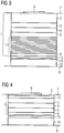
- the semiconductor chip comprises a semiconductor layer sequence 1 with an n-side current spreading layer 2, an n-cladding layer 3, an active region 4, a p-cladding layer 5 and a p-contact layer 6.
- the active region 4 is between the p-cladding layer 5 and the n-type cladding layer 3 is arranged, the n-type cladding layer 3 being arranged between the active region 4 and the radiation-emitting front side 7 of the semiconductor chip and the p-cladding layer 5 between the active region 4 and the backside 8 of the semiconductor chip.
- the p-contact layer 6 is applied to the side of the p-type cladding layer 5, which faces the rear side 8 of the semiconductor chip, while the current spreading layer 2 is arranged downstream of the n-type cladding layer 3 in the emission direction of the semiconductor chip.
- a front-side electrical bonding pad 9 is applied to the current spreading layer 2, from which contact fingers extend laterally over the front side 7 of the semiconductor chip (not shown in the figure) and onto which a bonding wire for electrically contacting the semiconductor chip to an electrically conductive region of a housing or a circuit board can be applied.
- the Semiconductor chip also be provided to be electrically contacted on the front side waiving a bonding wire, for example by means of an electrically conductive layer which connects the front side 7 of the semiconductor chip with an electrically conductive portion of a housing or a circuit board electrically conductive.
- a TCO contact layer 13 is applied to the side of the p-contact layer 6 pointing to the rear side 8 of the semiconductor chip and is connected to a TCO support substrate 10 without any fushing, for example by means of diffusion bonding or direct bonding.
- the TCO support substrate 10 comprises a material from the group of TCOs and is therefore electrically conductive and permeable to the radiation of the semiconductor chip. Furthermore, the material of the TCO contact layer does not necessarily have to match the material of the TCO supporting substrate.
- the semiconductor layer sequence 1 is based here on a phosphide compound semiconductor material.
- the active region 4 comprises, for example, undoped InGaAlP, has a thickness of between 100 nm and 1 ⁇ m and, during operation, generates electromagnetic radiation from the yellow to red spectral range of the visible light.
- the n-type cladding layer 3 comprises n-doped InAlP and the p-type cladding layer 5 p-doped InAlP.
- the cladding layers 3, 5 each have a thickness of between 200 nm and 1 ⁇ m.
- the p-contact layer 6 comprises highly p-doped AlGaAs and is between 50 nm and 200 nm thick.
- the current spreading layer 2 comprises InGaAlP or AlGaAs, and preferably has a thickness between 1 ⁇ m and 10 ⁇ m.
- the TCO contact layer 13 comprises a TCO, in this case, for example, with 2% aluminum-doped zinc oxide and has a thickness between 50 nm and 2000 nm.
- the active region 4 for radiation generation comprises, for example, a pn junction, a double heterostructure, a single quantum well or a multiple quantum well structure.
- the purpose of the n-cladding layer 3 and the p-cladding layer 5 is to confine the respective charge carriers to the active region 4.
- the p-contact layer 6 also serves to produce an improved electrical contact, preferably with an ohmic characteristic, between the TCO contact layer 13 and the semiconductor layer sequence 1, while with the aid of the current spreading layer 2, current which is impressed into the semiconductor chip via the front-side bonding pad 9, lateral as evenly as possible in the semiconductor layer sequence 1 and in particular in the active radiation-generating region 4 is distributed.
- the semiconductor layer sequence 1 is epitaxially grown, for example, on a GaAs growth substrate.
- the TCO contact layer 13 is attached to the side of the p-contact layer 6 facing the rear side 8 of the semiconductor chip.
- This can be applied epitaxially, for example, by sputtering, vapor deposition or with the aid of a sol-gel process.
- Sol-gel processes for applying TCO layers are for example in the publications DE 197 19 162 A1 and L. Spanhel et al., "Semiconductor Clusters in Sol-Gel Process: Quantized Aggregation, Gelation and Crystal Growth in Concentrated ZnO Colloids, J. Am. Chem. Soc. (1991), 113, 2826-2833 described.
- a TCO support substrate 10 for example, ZnO or ITO with a thickness between 50 .mu.m and 200 .mu.m by means of diffusion bonding applied.
- the boundary surfaces of the TCO support substrate 10 and the TCO contact layer 13 are brought into contact with each other and applied at temperatures between 1075 ° C and 1525 ° C and pressure in the range of yield stress of joining partners for a few hours, so that a cohesive, mechanically stable connection between the TCO contact layer 13 and the TCO support substrate 10 is formed.
- an electrically conductive connection between the TCO contact layer 13 and the TCO support substrate 10 is also advantageously formed.
- the growth substrate is thinned or removed, for example, by grinding and / or selective wet chemical etching.
- the semiconductor chip in the modification according to the FIG. 2 a roughened front side 7, which can be produced for example by etching.
- the roughening of the front side of the semiconductor chip 7 allows a better decoupling of the radiation from the semiconductor chip in the environment, since radiation losses due to multiple reflection at the interfaces semiconductor body / environment are usually reduced.
- the rear side 8 of the semiconductor chip comprises the modification according to FIG. 2 a metal layer 14, which is provided to improve the electrical contact to a conductive adhesive or solder, by means of which the semiconductor chip is mounted in a housing or on a circuit board at a later time. Furthermore, the metal layer 14 reflects radiation generated within the semiconductor layer sequence 1 back into it.
- the metal layer 14 has, for example, gold or aluminum.
- a TCO layer 15 which in the present case has substantially the same TCO material as the TCO support substrate 10, namely ZnO.
- the TCO support substrate 10 is bonded to the TCO layer 15 by direct bonding.
- the surfaces to be joined of the joining partners generally have to have roughnesses which are less than or equal to one nanometer. If this is not the case, the surfaces to be joined of the joining partners are polished accordingly. If the TCO layer 15 has to be polished, this must be taken into account when choosing its thickness.
- TCO support substrate 10 and TCO layer 15 are brought into direct contact with one another and exposed to temperatures between 300 ° C. and 1000 ° C. for a few hours, so that a cohesive, mechanically stable connection between TCO support substrate 10 and TCO layer 15 is formed.
- This usually forms Advantageously, an electrically conductive connection between TCO contact layer 13 and the TCO support substrate 10 from.
- pressurization can also take place up to about 20 bar. However, this is usually not mandatory.
- the TCO layer 15 can be used not only as an alternative to the TCO contact layer 13, but also in addition.
- the TCO contact layer 13 is disposed either between the p-type contact layer 6 and the TCO layer 15 or between the TCO layer 15 and the TCO supporting substrate 10.
- the surfaces to be joined can be heavily n-doped, for example with one of the n-dopants already mentioned in the general description part, in order to improve the electrical contact between the TCO support substrate 10 and the semiconductor layer sequence 1.
- the semiconductor chip of the embodiment according to the FIG. 3 a reflective layer, in the present case a DBR mirror 11, which is arranged between the p-type cladding layer 5 and the p-type contact layer 6.
- the DBR mirror 11 has a series of layers, in the present case between ten and twenty, which alternately have a high and a low refractive index.
- the DBR mirror for reflecting the radiation from the yellow to red spectral range of visible light for example, based on AlGaAs or AlGaInP, wherein in each case by varying the Al and the Ga content of the layers, the refractive indices are varied alternately.
- the Hableiterchip according to the FIG. 3 in contrast to the semiconductor chip according to the FIG. 1 an adhesive layer 16 disposed between the TCO contact layer 13 and the TCO support substrate 10.
- the adhesive layer 16 contains, for example, an electrically conductive, preferably for the radiation of the semiconductor chip permeable adhesive.
- the semiconductor layer sequence 1 can alternatively also be attached to the TCO support substrate 10 by means of an electrically insulating adhesive, such as BCB.
- an electrically insulating adhesive such as BCB.
- the roughnesses of the surfaces to be joined are at least in the range of a few nm.
- the adhesive layer 16 is made so thin that only between elevations due to the roughness of the surfaces to be joined, adhesive is contained, while the surfaces at the elevations in direct are in mechanical contact with each other such that an electrically conductive contact is formed between the surfaces.
- an electrically insulating adhesive for example, BCB
- BCB electrically insulating adhesive
- the semiconductor chip comprises in contrast to the embodiment according to the FIG. 1 an n-contact layer 12 of highly n-doped AlGaAs with a thickness of between 50 and 200 nm, which is arranged on the side of the n-cladding layer 3 facing the front side 7 of the semiconductor chip.
- the n-contact layer 12, as seen from the semiconductor layer sequence 1, is followed by an n-side current spreading layer 2 which comprises a TCO and has a thickness of between 200 nm and 1 ⁇ m.
- contact points may be arranged between these two layers, for example of Au / Ge (in the figure not shown).
- a TCO contact layer 13 including a TCO is disposed between the p-type contact layer 6 and the TCO supporting substrate 10.
- the TCO contact layer 13 does not necessarily have the same material as the TCO support substrate 10 and contributes to improved electrical contact with preferably ohmic characteristics between the TCO support substrate 10 and the semiconductor layer sequence 1.
- the TCO support substrate 10 may be attached to the semiconductor layer sequence by, for example, direct bonding or diffusion bonding. Alternatively, the TCO support substrate 10 may also be attached by gluing to the semiconductor layer sequence.
Landscapes
- Engineering & Computer Science (AREA)
- Computer Hardware Design (AREA)
- Microelectronics & Electronic Packaging (AREA)
- Power Engineering (AREA)
- Manufacturing & Machinery (AREA)
- Physics & Mathematics (AREA)
- Condensed Matter Physics & Semiconductors (AREA)
- Electromagnetism (AREA)
- General Physics & Mathematics (AREA)
- Led Devices (AREA)
- Led Device Packages (AREA)
- Photo Coupler, Interrupter, Optical-To-Optical Conversion Devices (AREA)
Claims (9)
- Puce à semi-conducteur optoélectronique, laquelle, en fonctionnement, émet un rayonnement électromagnétique depuis son côté avant (7), comprenant :- une succession de couches semi-conductrices (1) comprenant une zone active (4) qui est apte à générer le rayonnement électromagnétique, et- un substrat de support TCO (10) fabriqué séparément, disposé sur la succession de couches semi-conductrices, lequel présente un matériau du groupe des oxydes transparents conducteurs (TCO) et soutient mécaniquement la succession de couches semi-conductrices (1),dans laquelle
entre la succession de couches semi-conductrices (1) et le substrat de support TCO (10) est disposée une couche de contact TCO (13) qui établit un contact électrique entre la succession de couches semi-conductrices (1) et le substrat de support TCO (10) et présente un matériau du groupe des oxydes transparents conducteurs (TCO), et dans laquelle la couche de contact TCO (13) présente une épaisseur ≥ 1 µm et ≤ 5 µm. - Puce à semi-conducteur optoélectronique selon la revendication 1, dans laquelle le substrat de support TCO présente un indice de réfraction qui est inférieur à l'indice de réfraction de la succession de couches semi-conductrices.
- Puce à semi-conducteur optoélectronique selon l'une quelconque des revendications ci-dessus, dans laquelle le substrat de support TCO (10) est appliqué sur la succession de couches semi-conductrices par liaison directe, par liaison par diffusion ou par collage.
- Puce à semi-conducteur optoélectronique selon l'une quelconque des revendications ci-dessus, dans laquelle une couche réfléchissant le rayonnement de la puce à semi-conducteur est disposée entre la zone active (4) de la succession de couches semi-conductrices (1) et le substrat de support TCO (10).
- Puce à semi-conducteur optoélectronique selon la revendication 4, dans laquelle la couche réfléchissante est un miroir DBR (11) (Distributed Bragg Reflector Mirror) .
- Puce à semi-conducteur optoélectronique selon l'une quelconque des revendications ci-dessus, dans laquelle un côté arrière (8) de la puce à semi-conducteur, qui est disposé à l'opposé du côté avant (7) de celle-ci, comprend une couche métallique (14).
- Puce à semi-conducteur optoélectronique selon la revendication 6, dans laquelle la couche métallique (14) est réalisée de manière réfléchissante pour le rayonnement de la puce à semi-conducteur.
- Puce à semi-conducteur optoélectronique selon l'une quelconque des revendications ci-dessus, dont le côté avant (7) est rugueux.
- Puce à semi-conducteur optoélectronique selon l'une quelconque des revendications ci-dessus, dans laquelle, sur le côté de la succession de couches semi-conductrices (1), tourné vers le côté avant (7) de la puce à semi-conducteur, est disposée une couche d'élargissement de courant (2), laquelle présente un matériau du groupe des TCO.
Applications Claiming Priority (3)
| Application Number | Priority Date | Filing Date | Title |
|---|---|---|---|
| DE102005046691 | 2005-09-29 | ||
| DE102006023685A DE102006023685A1 (de) | 2005-09-29 | 2006-05-19 | Optoelektronischer Halbleiterchip |
| PCT/DE2006/001616 WO2007036198A2 (fr) | 2005-09-29 | 2006-09-14 | Puce a semi-conducteur optoelectronique |
Publications (2)
| Publication Number | Publication Date |
|---|---|
| EP1929551A2 EP1929551A2 (fr) | 2008-06-11 |
| EP1929551B1 true EP1929551B1 (fr) | 2018-06-27 |
Family
ID=37781828
Family Applications (1)
| Application Number | Title | Priority Date | Filing Date |
|---|---|---|---|
| EP06818008.2A Expired - Fee Related EP1929551B1 (fr) | 2005-09-29 | 2006-09-14 | Puce a semi-conducteur optoelectronique |
Country Status (7)
| Country | Link |
|---|---|
| US (1) | US8158995B2 (fr) |
| EP (1) | EP1929551B1 (fr) |
| JP (1) | JP2009510737A (fr) |
| KR (1) | KR20080068831A (fr) |
| DE (1) | DE102006023685A1 (fr) |
| TW (1) | TWI338379B (fr) |
| WO (1) | WO2007036198A2 (fr) |
Families Citing this family (8)
| Publication number | Priority date | Publication date | Assignee | Title |
|---|---|---|---|---|
| TWI460881B (zh) | 2006-12-11 | 2014-11-11 | Univ California | 透明發光二極體 |
| EP2174351A1 (fr) * | 2007-07-26 | 2010-04-14 | The Regents of the University of California | Diodes electroluminescentes avec surface de type p |
| DE102008019268A1 (de) | 2008-02-29 | 2009-09-03 | Osram Opto Semiconductors Gmbh | Optoelektronisches Bauelement und Verfahren zur Herstellung eines optoelektronischen Bauelements |
| DE102008027045A1 (de) * | 2008-02-29 | 2009-09-03 | Osram Opto Semiconductors Gmbh | Halbleiterleuchtdiode und Verfahren zur Herstellung einer Halbleiterleuchtdiode |
| DE102008032318A1 (de) * | 2008-03-31 | 2009-10-01 | Osram Opto Semiconductors Gmbh | Optoelektronischer Halbleiterchip und Verfahren zur Herstellung eines solchen |
| DE102009007625A1 (de) * | 2008-11-14 | 2010-05-20 | Osram Opto Semiconductors Gmbh | Verbundsubstrat für einen Halbleiterchip |
| WO2011074407A1 (fr) * | 2009-12-18 | 2011-06-23 | Semiconductor Energy Laboratory Co., Ltd. | Dispositif à semi-conducteur et procédé de fabrication associé |
| US8957440B2 (en) * | 2011-10-04 | 2015-02-17 | Cree, Inc. | Light emitting devices with low packaging factor |
Family Cites Families (25)
| Publication number | Priority date | Publication date | Assignee | Title |
|---|---|---|---|---|
| US5376580A (en) | 1993-03-19 | 1994-12-27 | Hewlett-Packard Company | Wafer bonding of light emitting diode layers |
| US5724376A (en) * | 1995-11-30 | 1998-03-03 | Hewlett-Packard Company | Transparent substrate vertical cavity surface emitting lasers fabricated by semiconductor wafer bonding |
| US5684309A (en) | 1996-07-11 | 1997-11-04 | North Carolina State University | Stacked quantum well aluminum indium gallium nitride light emitting diodes |
| KR100660152B1 (ko) | 1997-01-09 | 2006-12-21 | 니치아 카가쿠 고교 가부시키가이샤 | 질화물반도체소자 |
| US5831277A (en) | 1997-03-19 | 1998-11-03 | Northwestern University | III-nitride superlattice structures |
| DE19719162C2 (de) | 1997-05-06 | 2001-02-08 | Fraunhofer Ges Forschung | Verfahren zur Herstellung einer elektrisch leitenden ZnO enthaltenden Schicht auf einem Substrat |
| DE59814431D1 (de) | 1997-09-29 | 2010-03-25 | Osram Opto Semiconductors Gmbh | Halbleiterlichtquelle und Verfahren zu ihrer Herstellung |
| DE19955747A1 (de) | 1999-11-19 | 2001-05-23 | Osram Opto Semiconductors Gmbh | Optische Halbleitervorrichtung mit Mehrfach-Quantentopf-Struktur |
| JP5231701B2 (ja) * | 2000-02-15 | 2013-07-10 | オスラム オプト セミコンダクターズ ゲゼルシャフト ミット ベシュレンクテル ハフツング | 放射線を発する半導体デバイス及びその製造方法 |
| EP1277240B1 (fr) * | 2000-04-26 | 2015-05-20 | OSRAM Opto Semiconductors GmbH | Procédé de fabrication d'un composant semi-conducteur emetteur de lumière |
| TW513820B (en) | 2001-12-26 | 2002-12-11 | United Epitaxy Co Ltd | Light emitting diode and its manufacturing method |
| EP2262007B1 (fr) * | 2002-01-28 | 2016-11-23 | Nichia Corporation | Dispositif à semi-conducteur à base de nitrure comprenant un substrat de support |
| TW567618B (en) * | 2002-07-15 | 2003-12-21 | Epistar Corp | Light emitting diode with adhesive reflection layer and manufacturing method thereof |
| JP4787496B2 (ja) * | 2002-08-28 | 2011-10-05 | モクストロニクス,インコーポレイテッド | ハイブリッドビーム堆積システム及び方法並びにそれによって作製された半導体デバイス |
| US7041529B2 (en) * | 2002-10-23 | 2006-05-09 | Shin-Etsu Handotai Co., Ltd. | Light-emitting device and method of fabricating the same |
| TW565957B (en) | 2002-12-13 | 2003-12-11 | Ind Tech Res Inst | Light-emitting diode and the manufacturing method thereof |
| US7061065B2 (en) * | 2003-03-31 | 2006-06-13 | National Chung-Hsing University | Light emitting diode and method for producing the same |
| US7274000B2 (en) | 2003-07-11 | 2007-09-25 | Lincoln Global, Inc. | Power source for high current welding |
| US20050173724A1 (en) | 2004-02-11 | 2005-08-11 | Heng Liu | Group III-nitride based LED having a transparent current spreading layer |
| TW200528536A (en) * | 2003-12-19 | 2005-09-01 | Showa Denko Kk | Boron-containing polymer compound and organic light emitting device using the same |
| TWI288486B (en) * | 2004-03-17 | 2007-10-11 | Epistar Corp | Light-emitting diode and method for manufacturing the same |
| TWI232604B (en) | 2004-07-23 | 2005-05-11 | Supernova Optoelectronics Corp | Manufacturing method of metal reflection layer for gallium nitride based light-emitting diode |
| TWI280039B (en) | 2004-09-03 | 2007-04-21 | Teco Image Sys Co Ltd | Light reflecting structure |
| TWI240443B (en) * | 2004-12-17 | 2005-09-21 | South Epitaxy Corp | Light-emitting diode and method for manufacturing the same |
| DE102006028692B4 (de) | 2006-05-19 | 2021-09-02 | OSRAM Opto Semiconductors Gesellschaft mit beschränkter Haftung | Elektrisch leitende Verbindung mit isolierendem Verbindungsmedium |
-
2006
- 2006-05-19 DE DE102006023685A patent/DE102006023685A1/de not_active Withdrawn
- 2006-09-14 KR KR1020087010330A patent/KR20080068831A/ko not_active Application Discontinuation
- 2006-09-14 WO PCT/DE2006/001616 patent/WO2007036198A2/fr active Application Filing
- 2006-09-14 JP JP2008532583A patent/JP2009510737A/ja active Pending
- 2006-09-14 US US11/992,815 patent/US8158995B2/en not_active Expired - Fee Related
- 2006-09-14 EP EP06818008.2A patent/EP1929551B1/fr not_active Expired - Fee Related
- 2006-09-26 TW TW095135466A patent/TWI338379B/zh not_active IP Right Cessation
Non-Patent Citations (1)
| Title |
|---|
| None * |
Also Published As
| Publication number | Publication date |
|---|---|
| EP1929551A2 (fr) | 2008-06-11 |
| TWI338379B (en) | 2011-03-01 |
| JP2009510737A (ja) | 2009-03-12 |
| TW200721549A (en) | 2007-06-01 |
| WO2007036198A3 (fr) | 2007-05-24 |
| US20100264434A1 (en) | 2010-10-21 |
| WO2007036198A2 (fr) | 2007-04-05 |
| DE102006023685A1 (de) | 2007-04-05 |
| US8158995B2 (en) | 2012-04-17 |
| KR20080068831A (ko) | 2008-07-24 |
Similar Documents
| Publication | Publication Date | Title |
|---|---|---|
| EP1929551B1 (fr) | Puce a semi-conducteur optoelectronique | |
| EP1977457B1 (fr) | Puce a semi-conducteurs opto-electronique | |
| EP1277241B1 (fr) | Puce a diode electroluminescente a base de gan | |
| DE10211531B4 (de) | Hocheffiziente LED und Verfahren zur Herstellung derselben | |
| EP1284026A1 (fr) | Puce de diode electroluminescente dotee d'une suite de couches epitaxiales emettant des rayonnements et basees sur gan, et son procede de fabrication | |
| EP2057696B1 (fr) | Puce de semiconducteur optoélectronique et procédé de sa fabrication | |
| WO2008135013A2 (fr) | Puce semi-conductrice et procédé de fabrication d'une puce semi-conductrice | |
| DE102008009769A1 (de) | Doppel-Flip-Halbleiterbauelement und Herstellungsverfahren | |
| DE112006002083T5 (de) | Halbleiter-Leuchtvorrichtung und ihr Herstellungsverfahren | |
| EP1929552B1 (fr) | Élément semi-conducteur optoélectronique doté d'une couche d'étalement du courant | |
| EP2273574B1 (fr) | Procédé de fabrication d'un composant à diodes luminescentes doté d'une puce à diode luminescente à base de GaN | |
| EP2011161A2 (fr) | Composant à semi-conducteurs opto-électronique | |
| DE102010032497A1 (de) | Strahlungsemittierender Halbleiterchip und Verfahren zur Herstellung eines strahlungsemittierenden Halbleiterchips | |
| WO2018138081A1 (fr) | Puce semi-conductrice optoélectronique | |
| EP1770792B1 (fr) | Puce à semi-conducteur émetteur de lumière | |
| WO2012107289A1 (fr) | Puce semiconductrice optoélectronique à couche miroir encapsulée | |
| EP1299909B1 (fr) | Puce a diode electroluminescente a base d'ingan et son procede de fabrication | |
| DE102008015253B4 (de) | Verfahren zur Herstellung eines Laserbauelements und Laserbauelement | |
| EP1929550A1 (fr) | Puce a semi-conducteur opto-electronique | |
| WO2019002097A1 (fr) | Puce semi-conductrice pourvue d'une couche d'étalement du courant transparente | |
| DE102011012262A1 (de) | Optoelektronisches Halbleiterbauelement und Verfahren zur Herstellung eines optoelektronischen Halbleiterbauelements | |
| DE102007035896A1 (de) | Optoelektronischer Halbleiterkörper und optoelektronisches Bauelement | |
| DE10325603A1 (de) | Elektrisch leitfähiger Bondpad | |
| WO2014111384A1 (fr) | Puce semi-conductrice optoélectronique |
Legal Events
| Date | Code | Title | Description |
|---|---|---|---|
| PUAI | Public reference made under article 153(3) epc to a published international application that has entered the european phase |
Free format text: ORIGINAL CODE: 0009012 |
|
| 17P | Request for examination filed |
Effective date: 20080205 |
|
| AK | Designated contracting states |
Kind code of ref document: A2 Designated state(s): DE |
|
| RAP1 | Party data changed (applicant data changed or rights of an application transferred) |
Owner name: OSRAM OPTO SEMICONDUCTORS GMBH |
|
| RBV | Designated contracting states (corrected) |
Designated state(s): DE |
|
| DAX | Request for extension of the european patent (deleted) | ||
| 17Q | First examination report despatched |
Effective date: 20130813 |
|
| REG | Reference to a national code |
Ref country code: DE Ref legal event code: R079 Ref document number: 502006015938 Country of ref document: DE Free format text: PREVIOUS MAIN CLASS: H01L0033000000 Ipc: H01L0033420000 |
|
| GRAP | Despatch of communication of intention to grant a patent |
Free format text: ORIGINAL CODE: EPIDOSNIGR1 |
|
| RIC1 | Information provided on ipc code assigned before grant |
Ipc: H01L 33/42 20100101AFI20180126BHEP Ipc: H01L 33/00 20100101ALI20180126BHEP |
|
| INTG | Intention to grant announced |
Effective date: 20180306 |
|
| GRAS | Grant fee paid |
Free format text: ORIGINAL CODE: EPIDOSNIGR3 |
|
| GRAA | (expected) grant |
Free format text: ORIGINAL CODE: 0009210 |
|
| AK | Designated contracting states |
Kind code of ref document: B1 Designated state(s): DE |
|
| REG | Reference to a national code |
Ref country code: DE Ref legal event code: R096 Ref document number: 502006015938 Country of ref document: DE |
|
| REG | Reference to a national code |
Ref country code: DE Ref legal event code: R097 Ref document number: 502006015938 Country of ref document: DE |
|
| PLBE | No opposition filed within time limit |
Free format text: ORIGINAL CODE: 0009261 |
|
| STAA | Information on the status of an ep patent application or granted ep patent |
Free format text: STATUS: NO OPPOSITION FILED WITHIN TIME LIMIT |
|
| 26N | No opposition filed |
Effective date: 20190328 |
|
| PGFP | Annual fee paid to national office [announced via postgrant information from national office to epo] |
Ref country code: DE Payment date: 20210920 Year of fee payment: 16 |
|
| REG | Reference to a national code |
Ref country code: DE Ref legal event code: R119 Ref document number: 502006015938 Country of ref document: DE |
|
| PG25 | Lapsed in a contracting state [announced via postgrant information from national office to epo] |
Ref country code: DE Free format text: LAPSE BECAUSE OF NON-PAYMENT OF DUE FEES Effective date: 20230401 |