EP1927993A2 - Abnehmbarer Speicher mit Zeitschalter und integrierte Halbleiterschaltung - Google Patents
Abnehmbarer Speicher mit Zeitschalter und integrierte Halbleiterschaltung Download PDFInfo
- Publication number
- EP1927993A2 EP1927993A2 EP07253116A EP07253116A EP1927993A2 EP 1927993 A2 EP1927993 A2 EP 1927993A2 EP 07253116 A EP07253116 A EP 07253116A EP 07253116 A EP07253116 A EP 07253116A EP 1927993 A2 EP1927993 A2 EP 1927993A2
- Authority
- EP
- European Patent Office
- Prior art keywords
- time
- switch
- word line
- line system
- semiconductor
- Prior art date
- Legal status (The legal status is an assumption and is not a legal conclusion. Google has not performed a legal analysis and makes no representation as to the accuracy of the status listed.)
- Withdrawn
Links
Images


Classifications
-
- G—PHYSICS
- G11—INFORMATION STORAGE
- G11C—STATIC STORES
- G11C7/00—Arrangements for writing information into, or reading information out from, a digital store
-
- G—PHYSICS
- G11—INFORMATION STORAGE
- G11C—STATIC STORES
- G11C16/00—Erasable programmable read-only memories
- G11C16/02—Erasable programmable read-only memories electrically programmable
- G11C16/06—Auxiliary circuits, e.g. for writing into memory
- G11C16/22—Safety or protection circuits preventing unauthorised or accidental access to memory cells
-
- G—PHYSICS
- G06—COMPUTING OR CALCULATING; COUNTING
- G06F—ELECTRIC DIGITAL DATA PROCESSING
- G06F21/00—Security arrangements for protecting computers, components thereof, programs or data against unauthorised activity
- G06F21/10—Protecting distributed programs or content, e.g. vending or licensing of copyrighted material ; Digital rights management [DRM]
Definitions
- the present invention relates to removable storage which enables life time management without a power supply, and to a semiconductor integrated circuit.
- a flash memory is aboundingly used with spread of a digital camera or a mobile phone (see, e.g., Flash Memory Business Saizensen, Kyogyochosakai Publishing Co., Ltd. [Tokyo ]).
- a structure where a flash memory is accommodated in a package with a universal serial bus connector is aboundingly used because of facilitation of connection with a personal computer (a PC) and convenience in portability.
- Contents distribution using a cable television or the Internet has already spread, and a contents distribution service can be used any time as long as a subscribing download terminal is present.
- a subscriber cannot view/listen to contents by using, e.g., a personal computer or a mobile phone in a study room or an in-vehicle terminal if he/she does not have the download terminal.
- time-switch carrying removable storage which includes:
- Image information or audio information may be desirably provided in a fixed period alone in some cases. For example, that is a case of providing a viewable data in a broadcasting period of a serial broadcasting program or distributing new contents before a release day and disclosing the contents on the release day all at once.
- a semiconductor memory that stores information with a semiconductor time switch that controls a time can be considered.
- the present inventor has already given many reports about the semiconductor time switch as an aging device (see, e.g., JP-A 2004-94922 [KOKAI], JP-A 2004-172404 [KOKAI], JP-A 204,326,981 [KOKAI], US 7,075,284B2 and others).
- a solid state aging device (SSAD) will be first explained.
- FIGS. 7A and 7B are views showing a basic circuit system using the SSAD.
- the SSAD 3 is configured to be bridged ( FIG. 7A ) or clamped ( FIG. 7B ) between a memory 1 that records contents or secret information therein and a decoder 2 that reads the contents or the secret information.
- a function is the same, and both the structures can be freely selected in accordance with convenience in a circuit design.
- the SSAD 3 executes time management without a power supply, and controls access of the memory 1 and the decoder 2 to/from each other.
- information stored in the memory 1 can be read only in a validity period set in the SSAD 3 in advance. If the stored data is entertainment contents, the entertainment contents can be viewed/listened in the validity period alone.
- FIG. 8 shows an example of a basic structure that realizes the SSAD.
- a source region 21 and a drain region 22 are provided on a surface part of a silicon substrate 20 to interpose a gap therebetween, a floating gate 25 is formed on a channel 23 between the source region 21 and the drain region 22 via a tunnel insulating film (a first gate insulating film) 24, and a control gate 27 is formed on the floating gate 25 via an insulating film (a second gate insulating film) 26.
- a source electrode 28 and a drain electrode 29 are provided on the source region 21 and the drain region 22, respectively.
- a film thickness of the tunnel insulating film 24 is thinner than that in a general memory cell.
- a film thickness of a tunnel insulating film in a general memory cell is approximately 10 nm
- a film thickness of the tunnel insulating film in the memory cell used for the present aging device is as thin as 1 to 6 nm.
- the electrons when electrons are injected into the floating gate 25 at the time of initialization, the electrons diffuse to disappear with time.
- the channel region 23 is turned on at the time of initialization, and a space between the source electrode 28 and the drain electrode 29 is finally turned off. That is, this device constitutes a time switch without a power supply in which the source electrode 28 and the drain electrode 29 serve as input and output terminals.
- FIG. 9 briefly shows classifications of the normally-off type and the normally-on type.
- the normally-off type is in the off state before electric charges are injected into the gate.
- This type is previously turned on by injecting electric charges into the gate (initialization).
- the electric charges injected into the gate escape due to a leakage current, and an output signal is reduced with time.
- a graph of FIG. 10 shows such a state. Electrons are injected into the gate in case of a pMOSFET type, and holes are injected into the same in case of an nMOSFET. This realizes a function to "forget with a life time ⁇ 1".
- the normally-on type is in the on state due to impurity diffused in the channel in advance even before electric charges are injected into the gate.
- This type is previously turned off by injecting electric charges into the gate (initialization).
- the electric charges injected into the gate escape due to a leakage current, and an output signal is increased with time.
- a graph of FIG. 10B shows such a state.
- This graph shows a state where the channel is reversed at a time ⁇ 2 and the signal is precipitously increased. Holes are injected into the gate in case of the pMOSFET type, and electrons are injected into the same in case of the nMOSFET type. This realizes a function to "remember with a life time ⁇ 2".
- an aged change in a signal demonstrates a convex shape as shown in FIG. 11A when the condition ⁇ 2 ⁇ 1 is satisfied.
- an aged change in a signal demonstrates a concave shape as shown in FIG. 11B when the condition ⁇ 2> ⁇ 1 is satisfied.
- bit cost of a file memory when a security system is added to a semiconductor memory will now be considered.
- a result obtained by dividing a sum of a cost of a memory region and a cost of a security region by a bit number of a memory is a bit cost.
- the bit cost can be greatly reduced.
- an embedded memory having the SSAD added to a semiconductor memory will now be considered.
- a total bit number may be reduced several %, but it can be considered that the bit cost is lowered in whole.
- a NAND-type flash memory is currently spread as a file memory in a marketplace, this means that the bit cost with the security cost added thereto can be suppressed even if miniaturization of the NAND-type flash memory reaches its limit.
- a so-called'USB flash drive flash memory having a structure that the NAND flash memory is accommodated in a package including a universal serial bus connector has been widely used as removable storage.
- flash memory flash memory
- the SSAD flash memory
- it can be supplied to the marketplace as removable storage with a time limit. After the time limit is reached, new contents can be charged in this removable storage, or this removable storage can be reutilized as a regular removable storage.
- FIG. 1 is a view for explaining a basic concept of the present invention.
- a USB flash drive flash memory
- flash memory NAND flash with an SSAD satisfying the structure according to the present invention
- contents are stored in a memory cell array formed of the NAND flash, and the SSAD manages a validity limit of the contents. Since the SSAD can perform batteryless time management, a battery does not have to be mounted on the USB flash drive (flash memory). Further, this USB flash drive can be also utilized as a regular USB flash drive out of the validity period managed by the SSAD is reached.
- the removable storage with a low bit cost which enables a contents provider to set a time limit of contents and which can be also used as a general-purpose memory after end of the use limit, and the semiconductor integrated circuit.
- FIG. 2 is a block diagram showing a basic system of removable storage according to a first embodiment.
- This system includes a controller 113 that is accessed by a contents provider (a primary user) and a viewer (an end user) through an I/O terminal 115, a high-voltage (HV) system amplifying circuit (a word line system amplifying circuit) 109 that accepts an input from this controller 113, a low-voltage (LV) system amplifying circuit (a bit line system amplifying circuit, an sense amplifier) 111 that accepts an input from the controller 113, a bit line (BL) decoder 107 controlled by the LV system amplifying circuit 111, a word line (WL) decoder 105 controlled by the HV system amplifying circuit 109, a memory cell array 101 in which bit lines are controlled by the BL decoder 107 and word lines are controlled by the WL decoder, an SSAD 103 that is clamped between the LV system amplifying circuit 111 and the BL
- a cryptographic device 117 controls the initialization switch 119, the primary user who has a cryptographic key gives the key to the cryptographic device 117 through the controller 113 (the primary user and the cryptographic device 119 are directly connected with each other through a dotted line in the drawing for simplicity) to turn on the initialization switch 119, and the HV system amplifier 109 initializes (charges) the SSAD 103. At the end of this charging, contents are recorded in the memory cell array 101. The contents include a film, an image, a game, and others.
- the removable storage can be realized as an integrated circuit chip.
- the initialization switch 119 is inserted into a space between a well in a semiconductor substrate, e.g., a silicon substrate having the SSAD formed thereon and a well in the silicon substrate having each block in the memory cell array 101 formed thereon, and it serves as an initialization switch that is controlled to be opened/closed based on cryptographic.
- the integrated circuit chip can be accommodated in a package with a USB connector, and used as a so-called USB flash drive (flash memory).
- the end user does not own the cryptographic key, and can just read contents. It is presumed that the contents distributor manages the cryptographic key and the end user who sets up contracts with the contents distributor and views/listens to contents does not know about this cryptographic key.
- a user who manages the cryptographic key is the primary user, and a user who does not manage the cryptographic key is the end user. Additionally, it can be said that a user who does not present the cryptographic key is the end user.
- a person who owns the cryptographic key and accesses the controller 113 is regarded as an information provider
- a person who is allowed to write/erase data with respect to the memory cell array 101 and accesses the controller 113 without the cryptographic key is regarded as an information user
- reading information in the memory cell is allowed only in a desired period managed by the SSAD 103.
- the cryptographic device 117 may be software or hardware. In case of software, it is stored in a memory region (it may be a part of the memory cell array 101, but it may be also another memory region in the controller 113). When the primary user presents the cryptographic key to the controller 113, the controller 113 loads cryptographic software from the memory region and performs decryption by using the cryptographic key presented by the primary user.
- the SSAD 103 is initialized in this manner.
- the SSAD 103 just manages a time of viewing/listening or reading without using a battery, but it basically has four functions as explained in conjunction with FIGS. 10A, 10B, 11A, and 11B .
- access is enabled before a given life time, but access is disabled when the life time is exceeded ( FIG. 10A ).
- access is disabled before a given life time, but it is enabled when the life time is exceeded ( FIG. 10B ).
- access is disabled before a first life time, it is enabled in a period from the first life time to a second life time, and it is again disabled after the second life time ( FIG. 11A ).
- access is enabled before the first life time, but it is disabled in a period from the first life time to the second life time, and it is again enabled after the second life time ( FIG. 11B ).
- the system using the SSAD 103 can manage a contents reading period based on combinations of these four functions. Furthermore, since time management is carried out without a power supply, a battery does not have to be incorporated in the removable storage 100, and the system does not have to be connected with, e.g., a terminal that can receive power in order to manage the period. However, it is needless to say that power is supplied through the I/O terminal 115 when operating the removable storage 100 itself.
- this SSAD 103 manages access of the BL decoder 107 and the LV system amplifying circuit 111 to/from each other.
- the SSAD has a low impedance when its life time is ended, thereby disabling the function of the BL decoder 107.
- using the SSAD having the functions depicted in FIGS. 10A, 11A, and 11B means that the end user cannot read contents stored in the memory cell array 101 through the controller out of the contents reading period set in the SSAD 103.
- the primary user can use the cryptographic key that the end user does not know to control the HV system amplifying circuit through the controller 113 and reset the life time of the SSAD 103. That is, even if the validity period is once expired, the life time can be reset to prolong the reading period, or other contents can be recorded in the memory cell array 101 to set the life time.
- the LV system amplifying circuit 111 if access cannot be made to information because the life time is ended, i.e., if enabling reading is impossible out of the life time, the LV system amplifying circuit 111 cannot receive a signal from the BL decoder 107 when the end user tries accessing the memory cell array through the controller. At this time, the LV system amplifying circuit 111 can inform the controller 113 of the fact that receiving the signal from the BL decoder 107 has failed, and the controller 113 can command the HV system amplifying circuit to collectively erase (flash) information recorded in the memory cell array 101.
- the controller 113 when the controller 113 determines that access of the BL decoder 107 and the LV system amplifier 111 to/from each other is interrupted, the controller 113 can issue a command of concurrently writing information into a block having information recorded therein in the memory cell array 101 or all memory cells in the memory cell array 101 and erasing all of the recorded information through the WL decoder 105. In this case, expired information physically disappears from this world.
- the flash of memory can be realized by applying a high voltage to wells through the HV system to set all memory cells to "0". Specifically, applying a high voltage from the HV system amplifying circuit to the wells depicted in FIGS. 2 to 6 enables writing "0" in a memory cell in a corresponding block or all memory cells.
- the method of writing "1" into all memory cells through the word line decoder to erase information has been explained herein. This embodiment can select both the methods.
- a disruption of a signal from the BL decoder 107 enables flashing.
- a disruption of a signal from the word line decoder 105 enables flashing.
- flashing can be performed when a signal from the word line decoder 105 or the bit line decoder 107 is disrupted.
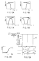
- FIG. 11 of this publication is selected and adopted in FIGS. 12A and 12B (however, reference numerals are changed).
- This semiconductor storage device 40 includes non-volatile memory cells 41, reset transistors 42 each of which is connected between a word line connected with a gate of the memory cell 41 and a booster 43, and an aging device 44 in which an input terminal is connected with the booster 43, an output terminal is connected with a gate of the transistor 42, an output signal becomes lower than a threshold value of the transistor 42 when data is read before end of a life time, and the output signal becomes higher than the threshold value of the transistor 42 after end of the life time.
- the transistor 42 When power is supplied after end of the life time of the aging device 44, the transistor 42 is turned on, and information stored in the memory cell 41 is reset.
- the aging circuit 44 it is preferable for the aging circuit 44 to be provided separately from the SSAD 103, but the HV system amplifying circuit 109 can be used as the booster 43. Replacing the memory cell 41 with a NAND cell is easy.
- the LV system amplifying circuit 111 when the end user tries accessing the memory cell array through the controller after end of the life time, the LV system amplifying circuit 111 cannot receive a signal from the BL decoder 107, but it can outputs a signal indicative of access denial from the SSAD 103. At this time, the LV system amplifying circuit 111 transfers this access denial signal to the controller 113, and the controller 113 can command the HV system amplifying circuit 109 to flash the memory cell array 101.
- a time limit of the removable storage can be set, thereby realizing the removable storage with a limit at a low bit cost.
- FIG. 3 is a block diagram of removable storage according to a second embodiment, and like reference numerals denote the same elements as those in the first embodiment, thus omitting a tautological explanation.
- an SSAD 103 having one of the functions depicted in FIGS. 10A, 10B, 11A, and 11B is bridged between a BL decoder 107 and an LV system amplifying circuit.
- the SSAD when the SSAD is in an non-access state (an off state), access of the BL decoder 107 and the LV system amplifying circuit to/from each other is turned off to disable a function of the BL decoder 107.
- an off state access of the BL decoder 107 and the LV system amplifying circuit to/from each other is turned off to disable a function of the BL decoder 107.
- the data carrier can be realized as an integrated circuit chip.
- the initialization switch 119 is inserted in a space between a well in a semiconductor substrate, e.g., a silicon substrate having the SSAD 103 formed thereon and a well in the silicon substrate having each block of the memory cell array 101 formed thereon, and functions as an initialization switch that is controlled to be opened/closed based on cryptography.
- the integrated circuit chip can be accommodated in a package having a USB connector, and used as a so-called USB flash drive.
- FIG. 4 is a block diagram of removable storage according to a third embodiment, and like reference numerals denote the same elements as those in the first embodiment, thereby omitting a tautological explanation.
- an SSAD 103 having one of the functions depicted in FIGS. 10A, 10B, 11A, and 11B is bridged between a WL decoder 105 and an HV system amplifying circuit 109.
- the WL decoder 105 When reading information stored in a memory cell array 101, the WL decoder 105 must switches on/off states of each memory transistor.
- the controller 113 when the controller 113 determines that access of the bit line decoder 107 and the bit line system amplifier 111 to/from each other is interrupted, the controller 113 can issue to the word line system amplifier 109 a command of concurrently writing information in a block having information recorded therein in the memory cell array 101 or all memory cells in the memory cell array 101 through the word line decoder 105 and erasing all recorded information.
- the removable storage can be realized as an integrated circuit chip.
- the initialization switch 119 is inserted into a space between a well in a semiconductor substrate, e.g., a silicon substrate having the SSAD 103 formed thereon and a well in the silicon substrate having each block of the memory cell array 101 formed thereon, and functions as an initialization switch that is controlled to be opened/closed based on cryptography.
- the integrated circuit chip can be accommodated in a package having a USB connector, and used as a so-called USB flash drive (flash memory).
- FIG. 5 is a block diagram of removable storage according to a fourth embodiment, and like reference numerals denote the same elements as those in the first embodiment, thereby omitting a tautological explanation.
- an SSAD 103 having one of the functions depicted in FIGS. 10A, 10B, 11A, and 11B is clamped between a WL decoder 105 and an HV system amplifying circuit 109.
- One end of an input/output terminal of the SSAD 103 serves as, e.g., a ground level. Therefore, the other end of the SSAD 103 connected with the WL decoder 105 also has a low impedance to disable a function of the WL decoder in the on-state of the SSAD 103.
- the controller 113 when the controller 113 determines that access of the bit line decoder 107 and the bit line system amplifier 111 to/from each other is interrupted, the controller 113 can issue to the word line system amplifier 109 a command of concurrently writing information in a block having information recorded therein in the memory cell array 101 or all memory cells in the memory cell array 101 through the word line decoder 105 and erasing all recorded information.
- the removable storage can be realized as an integrated circuit chip.
- the initialization switch 119 is inserted into a space between a well in a semiconductor substrate, e.g., a silicon substrate having the SSAD 103 formed thereon and a well in the silicon substrate having each block of the memory cell array 101 formed thereon, and functions as an initialization switch that is controlled to be opened/closed based on cryptography.
- the integrated circuit chip can be accommodated in a package having a USB connector, and used as a so-called USB flash drive (flash memory).
- FIG. 6 is a block diagram of removable storage according to a fifth embodiment, and like reference numerals denote the same elements as those in the first embodiment, thereby omitting a tautological explanation.
- an SSAD 103 having one of the functions depicted in FIGS. 10A, 10B, 11A, and 11B is clamped between a WL decoder 105 and an HV system amplifying circuit 109 and between a BL decoder 107 and an LV system amplifying circuit 111.
- the SSAD 103 enters an access state, one end of an input/output terminal of the SSAD 103 serves as a ground level. Therefore, the other end of the SSAD 103 connected with the WL decoder 105 and the BL decoder 107 also has a low impedance to disable functions of the WL decoder 105 and the BL decoder 107.
- the removable storage can be realized as an integrated circuit chip.
- the initialization switch 119 is inserted into a space between a well in a semiconductor substrate, e.g., a silicon substrate having the SSAD 103 formed thereon and a well in the silicon substrate having each block of the memory cell array 101 formed thereon, and functions as an initialization switch controlled to be opened/closed based on cryptography.
- the integrated circuit chip can be accommodated in a package having a USB connector, and used as a so-called USB flash drive (flash memory).
Landscapes
- Engineering & Computer Science (AREA)
- Theoretical Computer Science (AREA)
- Software Systems (AREA)
- Computer Security & Cryptography (AREA)
- Multimedia (AREA)
- Technology Law (AREA)
- Computer Hardware Design (AREA)
- Physics & Mathematics (AREA)
- General Engineering & Computer Science (AREA)
- General Physics & Mathematics (AREA)
- Read Only Memory (AREA)
- Storage Device Security (AREA)
- Static Random-Access Memory (AREA)
Applications Claiming Priority (1)
| Application Number | Priority Date | Filing Date | Title |
|---|---|---|---|
| JP2006324729A JP4212622B2 (ja) | 2006-11-30 | 2006-11-30 | 時限スイッチ付き情報担体及び半導体集積回路 |
Publications (2)
| Publication Number | Publication Date |
|---|---|
| EP1927993A2 true EP1927993A2 (de) | 2008-06-04 |
| EP1927993A3 EP1927993A3 (de) | 2008-10-01 |
Family
ID=38896877
Family Applications (1)
| Application Number | Title | Priority Date | Filing Date |
|---|---|---|---|
| EP07253116A Withdrawn EP1927993A3 (de) | 2006-11-30 | 2007-08-09 | Abnehmbarer Speicher mit Zeitschalter und integrierte Halbleiterschaltung |
Country Status (5)
| Country | Link |
|---|---|
| US (1) | US7813206B2 (de) |
| EP (1) | EP1927993A3 (de) |
| JP (1) | JP4212622B2 (de) |
| KR (1) | KR100908158B1 (de) |
| CN (1) | CN101241762A (de) |
Families Citing this family (7)
| Publication number | Priority date | Publication date | Assignee | Title |
|---|---|---|---|---|
| JP4435095B2 (ja) * | 2006-01-04 | 2010-03-17 | 株式会社東芝 | 半導体システム |
| US8140746B2 (en) * | 2007-12-14 | 2012-03-20 | Spansion Llc | Intelligent memory data management |
| JP5221172B2 (ja) * | 2008-02-29 | 2013-06-26 | 株式会社東芝 | Nand混載型半導体時限スイッチ |
| JP4717905B2 (ja) | 2008-05-28 | 2011-07-06 | アルプス電気株式会社 | 操作感触付与型入力装置 |
| US8260708B2 (en) * | 2009-04-17 | 2012-09-04 | Empire Technology Development Llc | Usage metering based upon hardware aging |
| WO2012015433A1 (en) | 2010-07-30 | 2012-02-02 | Empire Technology Development, Llc. | Aging-based usage metering of components |
| CN104995841B (zh) | 2013-01-06 | 2018-02-09 | 英派尔科技开发有限公司 | 基于老化的泄漏能量减小方法和系统 |
Citations (2)
| Publication number | Priority date | Publication date | Assignee | Title |
|---|---|---|---|---|
| EP1081577A2 (de) | 1999-08-31 | 2001-03-07 | Sony Corporation | Informationswiedergabe |
| EP1381159A2 (de) | 2002-07-08 | 2004-01-14 | Kabushiki Kaisha Toshiba | Vorrichtung zur Ausführung einer Zeit-Limitierungs-Funktion |
Family Cites Families (13)
| Publication number | Priority date | Publication date | Assignee | Title |
|---|---|---|---|---|
| JP3983969B2 (ja) * | 2000-03-08 | 2007-09-26 | 株式会社東芝 | 不揮発性半導体記憶装置 |
| JP2002196988A (ja) * | 2000-12-27 | 2002-07-12 | Sharp Corp | 記憶媒体 |
| JP4004811B2 (ja) * | 2002-02-06 | 2007-11-07 | 株式会社東芝 | 不揮発性半導体記憶装置 |
| JP3959340B2 (ja) | 2002-11-20 | 2007-08-15 | 株式会社東芝 | 半導体集積回路 |
| JP4068519B2 (ja) * | 2002-07-08 | 2008-03-26 | 株式会社東芝 | 有効期限付き機能利用装置 |
| JP4088195B2 (ja) * | 2003-04-28 | 2008-05-21 | 株式会社東芝 | 有効期限付き半導体記憶装置 |
| US8220064B2 (en) | 2004-07-20 | 2012-07-10 | Panasonic Corporation | Content management system and content management unit |
| WO2006008986A1 (ja) | 2004-07-23 | 2006-01-26 | Sharp Kabushiki Kaisha | 蓄積装置、方法、及び映像表示装置 |
| JP4489000B2 (ja) | 2005-10-12 | 2010-06-23 | 株式会社東芝 | 電子タイマー及びシステムlsi |
| JP4435095B2 (ja) | 2006-01-04 | 2010-03-17 | 株式会社東芝 | 半導体システム |
| JP2008103675A (ja) | 2006-09-22 | 2008-05-01 | Toshiba Corp | 半導体集積回路 |
| JP4469877B2 (ja) | 2007-07-12 | 2010-06-02 | 株式会社東芝 | 電子装置 |
| JP5221172B2 (ja) | 2008-02-29 | 2013-06-26 | 株式会社東芝 | Nand混載型半導体時限スイッチ |
-
2006
- 2006-11-30 JP JP2006324729A patent/JP4212622B2/ja not_active Expired - Fee Related
-
2007
- 2007-08-09 EP EP07253116A patent/EP1927993A3/de not_active Withdrawn
- 2007-08-27 US US11/845,451 patent/US7813206B2/en not_active Expired - Fee Related
- 2007-11-29 KR KR1020070123021A patent/KR100908158B1/ko not_active Expired - Fee Related
- 2007-11-30 CN CNA2007103062620A patent/CN101241762A/zh active Pending
Patent Citations (2)
| Publication number | Priority date | Publication date | Assignee | Title |
|---|---|---|---|---|
| EP1081577A2 (de) | 1999-08-31 | 2001-03-07 | Sony Corporation | Informationswiedergabe |
| EP1381159A2 (de) | 2002-07-08 | 2004-01-14 | Kabushiki Kaisha Toshiba | Vorrichtung zur Ausführung einer Zeit-Limitierungs-Funktion |
Also Published As
| Publication number | Publication date |
|---|---|
| JP4212622B2 (ja) | 2009-01-21 |
| US7813206B2 (en) | 2010-10-12 |
| CN101241762A (zh) | 2008-08-13 |
| EP1927993A3 (de) | 2008-10-01 |
| JP2008140051A (ja) | 2008-06-19 |
| KR20080049672A (ko) | 2008-06-04 |
| KR100908158B1 (ko) | 2009-07-16 |
| US20080133833A1 (en) | 2008-06-05 |
Similar Documents
| Publication | Publication Date | Title |
|---|---|---|
| US7813206B2 (en) | Time-switch carrying removable storage and semiconductor integrated circuit | |
| US10025596B2 (en) | Memory system for portable telephone | |
| KR100772246B1 (ko) | 반도체 장치 및 bios 인증 시스템 | |
| US7835183B2 (en) | Nonvolatile storage device and control method thereof | |
| US8787089B2 (en) | Semiconductor device and method of controlling the same | |
| US20140040537A1 (en) | Storage medium using nonvolatile semiconductor storage device, and data terminal including the same | |
| US7372743B2 (en) | Controlling a nonvolatile storage device | |
| US8365309B2 (en) | Memory device | |
| US8357965B2 (en) | Semiconductor device having multiple storage regions | |
| US20140040536A1 (en) | Storage medium using nonvolatile semiconductor storage device, data terminal having the storage medium mounted thereon, and file erasing method usable for the same | |
| US12579307B2 (en) | Control of debug port access to data in a memory device, operating method of the same, and memory system | |
| JP4916785B2 (ja) | 半導体記憶装置及びこれを備えた電子機器 | |
| JPH02249738A (ja) | プリセット情報記憶装置 | |
| JP2008140501A (ja) | 半導体メモリ |
Legal Events
| Date | Code | Title | Description |
|---|---|---|---|
| PUAI | Public reference made under article 153(3) epc to a published international application that has entered the european phase |
Free format text: ORIGINAL CODE: 0009012 |
|
| 17P | Request for examination filed |
Effective date: 20070817 |
|
| AK | Designated contracting states |
Kind code of ref document: A2 Designated state(s): AT BE BG CH CY CZ DE DK EE ES FI FR GB GR HU IE IS IT LI LT LU LV MC MT NL PL PT RO SE SI SK TR |
|
| AX | Request for extension of the european patent |
Extension state: AL BA HR MK RS |
|
| PUAL | Search report despatched |
Free format text: ORIGINAL CODE: 0009013 |
|
| AK | Designated contracting states |
Kind code of ref document: A3 Designated state(s): AT BE BG CH CY CZ DE DK EE ES FI FR GB GR HU IE IS IT LI LT LU LV MC MT NL PL PT RO SE SI SK TR |
|
| AX | Request for extension of the european patent |
Extension state: AL BA HR MK RS |
|
| 17Q | First examination report despatched |
Effective date: 20081112 |
|
| AKX | Designation fees paid |
Designated state(s): DE FR GB |
|
| GRAP | Despatch of communication of intention to grant a patent |
Free format text: ORIGINAL CODE: EPIDOSNIGR1 |
|
| STAA | Information on the status of an ep patent application or granted ep patent |
Free format text: STATUS: THE APPLICATION IS DEEMED TO BE WITHDRAWN |
|
| 18D | Application deemed to be withdrawn |
Effective date: 20110308 |