EP1900540A1 - Optischer datenträger und sputter-target für eine cu-legierungs-aufzeichnungsschicht - Google Patents
Optischer datenträger und sputter-target für eine cu-legierungs-aufzeichnungsschicht Download PDFInfo
- Publication number
- EP1900540A1 EP1900540A1 EP06731381A EP06731381A EP1900540A1 EP 1900540 A1 EP1900540 A1 EP 1900540A1 EP 06731381 A EP06731381 A EP 06731381A EP 06731381 A EP06731381 A EP 06731381A EP 1900540 A1 EP1900540 A1 EP 1900540A1
- Authority
- EP
- European Patent Office
- Prior art keywords
- recording layer
- zns
- optical disk
- alloy
- recording
- Prior art date
- Legal status (The legal status is an assumption and is not a legal conclusion. Google has not performed a legal analysis and makes no representation as to the accuracy of the status listed.)
- Granted
Links
Images

Classifications
-
- C—CHEMISTRY; METALLURGY
- C23—COATING METALLIC MATERIAL; COATING MATERIAL WITH METALLIC MATERIAL; CHEMICAL SURFACE TREATMENT; DIFFUSION TREATMENT OF METALLIC MATERIAL; COATING BY VACUUM EVAPORATION, BY SPUTTERING, BY ION IMPLANTATION OR BY CHEMICAL VAPOUR DEPOSITION, IN GENERAL; INHIBITING CORROSION OF METALLIC MATERIAL OR INCRUSTATION IN GENERAL
- C23C—COATING METALLIC MATERIAL; COATING MATERIAL WITH METALLIC MATERIAL; SURFACE TREATMENT OF METALLIC MATERIAL BY DIFFUSION INTO THE SURFACE, BY CHEMICAL CONVERSION OR SUBSTITUTION; COATING BY VACUUM EVAPORATION, BY SPUTTERING, BY ION IMPLANTATION OR BY CHEMICAL VAPOUR DEPOSITION, IN GENERAL
- C23C14/00—Coating by vacuum evaporation, by sputtering or by ion implantation of the coating forming material
- C23C14/22—Coating by vacuum evaporation, by sputtering or by ion implantation of the coating forming material characterised by the process of coating
- C23C14/34—Sputtering
- C23C14/3407—Cathode assembly for sputtering apparatus, e.g. Target
- C23C14/3414—Metallurgical or chemical aspects of target preparation, e.g. casting, powder metallurgy
-
- G—PHYSICS
- G11—INFORMATION STORAGE
- G11B—INFORMATION STORAGE BASED ON RELATIVE MOVEMENT BETWEEN RECORD CARRIER AND TRANSDUCER
- G11B7/00—Recording or reproducing by optical means, e.g. recording using a thermal beam of optical radiation by modifying optical properties or the physical structure, reproducing using an optical beam at lower power by sensing optical properties; Record carriers therefor
- G11B7/24—Record carriers characterised by shape, structure or physical properties, or by the selection of the material
- G11B7/241—Record carriers characterised by shape, structure or physical properties, or by the selection of the material characterised by the selection of the material
- G11B7/242—Record carriers characterised by shape, structure or physical properties, or by the selection of the material characterised by the selection of the material of recording layers
- G11B7/243—Record carriers characterised by shape, structure or physical properties, or by the selection of the material characterised by the selection of the material of recording layers comprising inorganic materials only, e.g. ablative layers
- G11B7/2433—Metals or elements of Groups 13, 14, 15 or 16 of the Periodic Table, e.g. B, Si, Ge, As, Sb, Bi, Se or Te
-
- G—PHYSICS
- G11—INFORMATION STORAGE
- G11B—INFORMATION STORAGE BASED ON RELATIVE MOVEMENT BETWEEN RECORD CARRIER AND TRANSDUCER
- G11B7/00—Recording or reproducing by optical means, e.g. recording using a thermal beam of optical radiation by modifying optical properties or the physical structure, reproducing using an optical beam at lower power by sensing optical properties; Record carriers therefor
- G11B7/24—Record carriers characterised by shape, structure or physical properties, or by the selection of the material
- G11B7/26—Apparatus or processes specially adapted for the manufacture of record carriers
- G11B7/266—Sputtering or spin-coating layers
Definitions
- the present invention generally relates to an optical disk and a sputtering target for a Cu alloy recording layer, and in particular relates to an optical disk and a sputtering target for a Cu alloy recording layer capable of obtaining an optical recording medium with no error in the recording bit when a protective layer containing ZnS (for instance, ZnS-SiO 2 ) is used.
- a protective layer containing ZnS for instance, ZnS-SiO 2
- This kind of optical disk records information by heating and increasing the temperature of a recording thin film on a substrate by irradiating a laser beam thereto, and generating a change in the structure of such recording thin film. More specifically, the reproduction of information is conducted by detecting the change in the reflectivity caused by the change in the optical constant.
- the aforementioned phase change is performed with the irradiation of a laser beam narrowed down to a diameter of approximately 1 to several ⁇ m.
- a 1 ⁇ m laser beam passes through at a linear velocity of 10m/S, light is irradiated to a certain point on the optical disk for 100ns, and it is necessary to generate the foregoing crystallographic change and detect reflectivity within such time frame.
- an optical disk has a structure where a recording layer is sandwiched by protective layers, or a structure where one side of a recording layer is covered with a protective layer.
- Non-Patent Document 1 Laser is irradiated to the Cu recording layer for reacting Cu and Si, and the crystal structure in the structure between Cu and Si is changed for recording. This is only for writing once, and no editing or rewriting is allowed.
- Non-Patent Document 1 it is a write-once disk of dual structure and inorganic material system with the use of blue laser light.
- This disk has a sandwich structure, where a Cu alloy layer is provided adjacent to a Si layer and the recording medium is sandwiched by protective layers. Further, this sandwich structure is formed as a dual structure via a spacer layer, and is disposed on a PC (polycarbonate) substrate via a reflective layer. A cover layer is provided on the surface layer.
- a Cu alloy recording layer is shown, there is no particular reference to the alloy component. Further, since a copper or a copper alloy recording layer is still in its infancy, the favorable aspects are not sufficiently unknown.
- a protective layer a material containing ZnS (for instance, ZnS-SiO 2 ) is used. Incidentally, the following example explains a case of using this ZnS-SiO 2 as the protective layer.
- the optimal strategy would be to devise the Cu recording layer so that it could prevent sulfuration on its own.
- Non-Patent Document 1 Hiroyasu Inoue (and four others) "Dual-Layer Inorganic Write-Once Disc based on Blu-ray Disc Format" International Symposium on Optical Memory 2003 11/3-7 Zenki Technical Digest P.50
- the present invention relates to an optical disk and a sputtering target for a Cu alloy recording layer.
- a protective layer consists of ZnS (for instance, ZnS-SiO 2 )
- this invention aims at providing the technology that prevents or inhibits sulfuration of the Cu recording layer caused by the dispersion of S from the protective layer and enables obtaining an optical recording medium with no error in the recording bit.
- the present invention provides the optical disk with a Cu alloy recording layer that contains one or more components selected from Zn, Mn, Ga, Ti and Ta in a total amount of 1 to 20at% and the remnants composed of Cu and inevitable impurities.
- This technology enables to effectively prevent the damage caused by S dispersing from a protective layer containing ZnS (for instance, ZnS-SiO 2 ), and the formation of opaque CuS and Cu 2 S caused by the sulfuration of Cu.
- ZnS for instance, ZnS-SiO 2
- the impurities composed of Mg, Na, Ca, Ba, Ce, Li and Zr existing in the Cu alloy recording layer are respectively 0.1 at% or less.
- impurities exist in excess of 0.1 at % it becomes difficult to inhibit the damage caused by S dispersing from a protective layer containing ZnS, and may contrarily promote the sulfuration of Cu.
- the present invention forms the Cu alloy recording layer through sputtering, and the sputtering target for the Cu alloy recording layer itself is made to be a copper alloy containing one or more components selected from Zn, Mn, Ga, Ti and Ta in a total amount of 1 to 20at%, and the remnants composed of Cu and inevitable impurities.
- the impurities composed of Mg, Na, Ca, Ba, Ce, Li and Zr existing in the Cu alloy are respectively 0.1 at% or less.
- the optical disk and the sputtering target for a Cu alloy recording layer of the present invention are capable of obtaining an optical recording medium that prevents or inhibits sulfuration of the Cu recording layer caused by the dispersion of S from the protective layer and is error free in the recording bit, particularly when a protective layer consists of ZnS (for instance, ZnS-SiO 2 ).
- a protective layer consists of ZnS (for instance, ZnS-SiO 2 ).
- the present invention yields superior effects as an optical disk and a sputtering target for a Cu alloy recording layer capable of high-speed recording and large-capacity writing.
- a dense oxide film is formed on the metal surface, and such dense oxide film is used to prevent oxidization from advancing any further.
- Al is a material with strong oxidizing power
- dense Al 2 O 3 is formed on the surface, oxidization will not advance any further, and this becomes a material with extremely superior corrosion resistance.
- MgO is also a similar material.
- additive agents to be added to the parent material it is considered effective to select a material in which the standard free energy of formation of oxides is small.
- B was selected as a material having standard free energy of formation of sulfides that is slightly higher than Cu.
- B is considerably higher than the standard free energy of formation of sulfides of Zn, but is only slightly lower or equal to Cu. In this case, as expected, the addition of B actually promoted the sulfuration of Cu (Comparative Example 3 described later).
- metal elements selected from Zn, Mn, Ga, Ti and Ta. Furthermore, the addition of these elements at 1 to 20at% is effective. It has become known that no effect will be yielded if the added amount is less than 1 at%, and it is undesirable to add these elements exceeding 20at% since the function as a Cu recording layer will deteriorate.
- ZnS is a stable compound when Zn and S are in a ratio of 1:1. Nevertheless, the composition will not necessarily be a stoichiometric composition of 1:1, and there are cases where the compositional range will be Zn-rich and S-rich.
- the activity of S of ZnS (value showing the activity ratio of S, and the larger the activity, the more sulfurized the component) is small, CuS or Cu 2 S which is unstable as sulfides is not formed, and thereby corrosion caused by sulfuration will not occur.
- composition when the composition is S-rich, the activity of S of ZnS is large, CuS or Cu 2 S which is unstable as sulfides is formed, and thereby corrosion caused by sulfuration will occur.
- ZnS of the composition used as a protective layer is formed through sputtering, and, when a S-rich portion is partially formed or the overall sputtering target is formed to be S-rich, the composition will be directly reflected on the film, and it is likely that a S-rich layer will be formed on the entire surface of the film. In this kind of case, a S-rich ZnS is considered to cause the corrosion of Cu.
- This additive agent is a metal element selected from Zn, Mn, Ga, Ti and Ta, and Zn and Mn are particularly effective. Since these sulfides themselves are transparent and do not absorb light, they do not deteriorate the function as a recording layer.
- Mg is an element that has small standard free energy of formation and forms stable sulfides, Mg promotes the dissociation of S from ZnS and makes ZnS unstable, and it is considered that Mg promotes the creation of active S and deteriorates the function as a protective film.
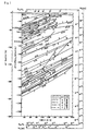
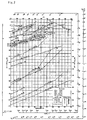
- Fig. 1 and Fig. 2 the relationship of the range of standard free energy of formation of sulfides and the temperature is shown in Fig. 1 and Fig. 2 .
- the source of Fig. 1 is Iron and Steel Handbook (3rd Edition), Volume 1, Page 12 "Basic Theory (Figs. 1 and 3(b) Relation of Standard Free Energy of Formation of Sulfides and Temperature),” and the Iron and Steel Institute of Japan, issued by Maruzen (October 30, 1981 ; Second Print).
- the source of Fig. 2 is Thermodynamics of Solids by Swalin, Figs. 7 and 8 " Relation of Standard Free Energy of Formation of Sulfides and Temperature," issued by Corona (March 25, 1992; 15th Print ).
- the elements that promote the creation of active S and deteriorate the function of a protective film due to dissociation of S from ZnS and destabilization of ZnS, and the elements that are not active enough to prevent the formation of CuS, are harmful as impurities in Cu.
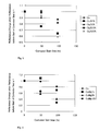
- the standard free energy of formation of ZnS at 300K is -112kcal/mol S2, and the anticorrosion effect when adding Zn as an additive material having the same standard free energy of formation of sulfides as ZnS was extremely high and favorable. Further, as shown in Fig. 3 , although the reflectance ratio decreased slightly than the corrosion test of Cu only in the long-term acceleration test of 100 hours with the additive amount of Zn at 20at%, the other tests hardly showed any decrease in the reflectance ratio, and it is evident that the addition of Zn is extremely effective.
- the anticorrosion test involved an acceleration test at constant temperature and humidity (85°C, 85%, 100 hours). The appearance of corrosion was compared by visual observation and reflectance ratio measurement before and after the acceleration test. The results of this anticorrosion test are shown in Table 1. Further, the reflectance ratio measured results are shown in Fig. 4 .
- ⁇ G of Ga is -117
- ⁇ G of Ti is -116
- ⁇ G of Ta is -102.
- the anticorrosion test involved an acceleration test at constant temperature and humidity (85°C, 85%, 100 hours). The appearance of corrosion was compared by visual observation and reflectance ratio measurement before and after the acceleration test. The results of this anticorrosion test are shown in Table 1. Further, the reflectance ratio measured results are shown in Fig. 5 .
- the anticorrosion test involved an acceleration test at constant temperature and humidity (85°C, 85%, 100 hours). The appearance of corrosion was compared by visual observation and reflectance ratio measurement before and after the acceleration test. The results of this anticorrosion test are shown in Table 1. Further, the reflectance ratio measured results are shown in Fig. 6 .
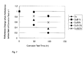
- the anticorrosion test involved an acceleration test at constant temperature and humidity (85°C, 85%, 100 hours). The appearance of corrosion was compared by visual observation and reflectance ratio measurement before and after the acceleration test. The results of this anticorrosion test are shown in Table 1. Further, the reflectance ratio measured results are shown in Fig. 7 .
- the optical disk and the sputtering target for a Cu alloy recording layer of the present invention are capable of obtaining an optical recording medium that prevents or inhibits sulfuration of the Cu recording layer caused by the dispersion of S from the protective layer and is error free in the recording bit, particularly when a protective layer consists of ZnS (for instance, ZnS-SiO 2 ).
- a protective layer consists of ZnS (for instance, ZnS-SiO 2 ).
- the present invention yields superior effects as an optical disk and a sputtering target for a Cu alloy recording layer capable of high-speed recording and large-capacity writing.
Landscapes
- Chemical & Material Sciences (AREA)
- Engineering & Computer Science (AREA)
- Chemical Kinetics & Catalysis (AREA)
- Materials Engineering (AREA)
- Mechanical Engineering (AREA)
- Metallurgy (AREA)
- Organic Chemistry (AREA)
- Inorganic Chemistry (AREA)
- Manufacturing & Machinery (AREA)
- Thermal Transfer Or Thermal Recording In General (AREA)
- Optical Record Carriers And Manufacture Thereof (AREA)
- Manufacturing Optical Record Carriers (AREA)
Applications Claiming Priority (2)
| Application Number | Priority Date | Filing Date | Title |
|---|---|---|---|
| JP2005195318 | 2005-07-04 | ||
| PCT/JP2006/307434 WO2007004344A1 (ja) | 2005-07-04 | 2006-04-07 | 光ディスク及びCu合金記録層用スパッタリングターゲット |
Publications (3)
| Publication Number | Publication Date |
|---|---|
| EP1900540A1 true EP1900540A1 (de) | 2008-03-19 |
| EP1900540A4 EP1900540A4 (de) | 2009-02-18 |
| EP1900540B1 EP1900540B1 (de) | 2010-03-03 |
Family
ID=37604220
Family Applications (1)
| Application Number | Title | Priority Date | Filing Date |
|---|---|---|---|
| EP06731381A Ceased EP1900540B1 (de) | 2005-07-04 | 2006-04-07 | Optischer datenträger und sputter-target für eine cu-legierungs-aufzeichnungsschicht |
Country Status (5)
| Country | Link |
|---|---|
| EP (1) | EP1900540B1 (de) |
| JP (1) | JP4603044B2 (de) |
| CN (1) | CN101218106B (de) |
| TW (1) | TW200706674A (de) |
| WO (1) | WO2007004344A1 (de) |
Families Citing this family (3)
| Publication number | Priority date | Publication date | Assignee | Title |
|---|---|---|---|---|
| JP5722427B2 (ja) * | 2011-03-01 | 2015-05-20 | Jx日鉱日石金属株式会社 | 銅チタン合金製スパッタリングターゲット、同スパッタリングターゲットを用いて形成した半導体配線並びに同半導体配線を備えた半導体素子及びデバイス |
| CN103774100A (zh) * | 2012-10-22 | 2014-05-07 | 中环股份有限公司 | 溅镀靶材及可写录光记录媒体 |
| JP5594618B1 (ja) * | 2013-02-25 | 2014-09-24 | 三菱マテリアル株式会社 | スパッタリングターゲット及びその製造方法 |
Family Cites Families (10)
| Publication number | Priority date | Publication date | Assignee | Title |
|---|---|---|---|---|
| FR2475270A1 (fr) * | 1980-02-01 | 1981-08-07 | Thomson Csf | Structure de memoire reversible, a inscription thermo-optique et lecture optique, et procede d'inscription et d'effacement de cette structure |
| JPS5938291B2 (ja) * | 1981-02-25 | 1984-09-14 | 株式会社東芝 | 色調記憶素子用合金 |
| JPH066393B2 (ja) * | 1984-03-07 | 1994-01-26 | 株式会社日立製作所 | 情報の記録・消去方法 |
| JPS61194658A (ja) * | 1985-02-22 | 1986-08-29 | Hitachi Ltd | 情報記録媒体 |
| JPS62247060A (ja) * | 1986-04-17 | 1987-10-28 | Mitsubishi Electric Corp | 光情報記録媒体 |
| JPH0256746A (ja) * | 1988-08-19 | 1990-02-26 | Matsushita Electric Ind Co Ltd | 情報担体ディスク |
| JPH0569671A (ja) * | 1991-09-13 | 1993-03-23 | Nec Corp | 多値光記録媒体およびその読み出し装置 |
| TW468179B (en) * | 1998-08-05 | 2001-12-11 | Matsushita Electric Industrial Co Ltd | Optical recording medium |
| JP2002172861A (ja) * | 2000-12-06 | 2002-06-18 | Ricoh Co Ltd | 光情報記録媒体 |
| JP2004079022A (ja) * | 2002-08-12 | 2004-03-11 | Tdk Corp | 光記録媒体及び光記録方法 |
-
2006
- 2006-04-07 CN CN2006800244989A patent/CN101218106B/zh not_active Expired - Fee Related
- 2006-04-07 EP EP06731381A patent/EP1900540B1/de not_active Ceased
- 2006-04-07 WO PCT/JP2006/307434 patent/WO2007004344A1/ja not_active Ceased
- 2006-04-07 JP JP2007523348A patent/JP4603044B2/ja not_active Expired - Fee Related
- 2006-04-14 TW TW095113343A patent/TW200706674A/zh not_active IP Right Cessation
Also Published As
| Publication number | Publication date |
|---|---|
| JP4603044B2 (ja) | 2010-12-22 |
| CN101218106B (zh) | 2010-05-26 |
| TW200706674A (en) | 2007-02-16 |
| JPWO2007004344A1 (ja) | 2009-01-22 |
| EP1900540A4 (de) | 2009-02-18 |
| WO2007004344A1 (ja) | 2007-01-11 |
| TWI312814B (de) | 2009-08-01 |
| CN101218106A (zh) | 2008-07-09 |
| EP1900540B1 (de) | 2010-03-03 |
Similar Documents
| Publication | Publication Date | Title |
|---|---|---|
| JP3907666B2 (ja) | レーザーマーキング用再生専用光情報記録媒体 | |
| JP4377861B2 (ja) | 光情報記録媒体用Ag合金反射膜、光情報記録媒体および光情報記録媒体用Ag合金反射膜の形成用のAg合金スパッタリングターゲット | |
| JP2006054032A5 (de) | ||
| JP2002015464A (ja) | 光情報記録媒体用の反射層または半透明反射層、光情報記録媒体及び光情報記録媒体用スパッタリングターゲット | |
| JP3655907B2 (ja) | 光情報記録媒体用反射膜と半透過反射膜、および光情報記録媒体 | |
| TWI336888B (en) | Silver alloy reflective films for optical information recording media, silver alloy sputtering targets therefor, and optical information recording media | |
| JP2007031743A (ja) | 光情報記録媒体用Ag合金反射膜及び光情報記録媒体 | |
| JP2006294195A (ja) | 光情報記録用Ag合金反射膜、光情報記録媒体および光情報記録用Ag合金反射膜の形成用のAg合金スパッタリングターゲット | |
| EP1900540B1 (de) | Optischer datenträger und sputter-target für eine cu-legierungs-aufzeichnungsschicht | |
| JP4153484B2 (ja) | 光情報記録媒体用Ag基合金スパッタリングターゲット | |
| JP2007062108A (ja) | 光情報記録媒体用の記録層およびスパッタリングターゲット、並びに光情報記録媒体 | |
| WO2007046390A1 (ja) | 光情報記録媒体用記録層、光情報記録媒体、および光情報記録媒体用スパッタリングターゲット | |
| US8105673B2 (en) | Sputtering target for optical media, method of manufacturing same, optical medium, and method of manufacturing same | |
| JP3924308B2 (ja) | レーザーマーキング用再生専用光情報記録媒体用Ag合金反射膜の形成用のAg合金スパッタリングターゲット | |
| JP4559490B2 (ja) | 光記録媒体 | |
| JP4252867B2 (ja) | 光学的情報記録媒体 | |
| JP5012984B2 (ja) | 光メディアの反射層用スパッタリングターゲット、及び、その製造方法 | |
| JP4336835B2 (ja) | 光学的情報記録媒体 | |
| JP4376842B2 (ja) | 光記録媒体 | |
| JP3620597B1 (ja) | 光情報記録媒体 | |
| JPWO2010095466A1 (ja) | 情報記録媒体 | |
| JP2007287302A (ja) | 光学的情報記録媒体 | |
| JP2008243312A (ja) | 情報記録媒体 | |
| JP2004164806A (ja) | 光記録媒体 |
Legal Events
| Date | Code | Title | Description |
|---|---|---|---|
| PUAI | Public reference made under article 153(3) epc to a published international application that has entered the european phase |
Free format text: ORIGINAL CODE: 0009012 |
|
| 17P | Request for examination filed |
Effective date: 20071214 |
|
| AK | Designated contracting states |
Kind code of ref document: A1 Designated state(s): CH LI NL |
|
| DAX | Request for extension of the european patent (deleted) | ||
| RBV | Designated contracting states (corrected) |
Designated state(s): CH LI NL |
|
| A4 | Supplementary search report drawn up and despatched |
Effective date: 20090116 |
|
| 17Q | First examination report despatched |
Effective date: 20090323 |
|
| GRAP | Despatch of communication of intention to grant a patent |
Free format text: ORIGINAL CODE: EPIDOSNIGR1 |
|
| GRAS | Grant fee paid |
Free format text: ORIGINAL CODE: EPIDOSNIGR3 |
|
| GRAA | (expected) grant |
Free format text: ORIGINAL CODE: 0009210 |
|
| AK | Designated contracting states |
Kind code of ref document: B1 Designated state(s): CH LI NL |
|
| REG | Reference to a national code |
Ref country code: CH Ref legal event code: NV Representative=s name: ISLER & PEDRAZZINI AG Ref country code: CH Ref legal event code: EP |
|
| REG | Reference to a national code |
Ref country code: NL Ref legal event code: T3 |
|
| PLBE | No opposition filed within time limit |
Free format text: ORIGINAL CODE: 0009261 |
|
| STAA | Information on the status of an ep patent application or granted ep patent |
Free format text: STATUS: NO OPPOSITION FILED WITHIN TIME LIMIT |
|
| REG | Reference to a national code |
Ref country code: NL Ref legal event code: SD Effective date: 20110111 |
|
| 26N | No opposition filed |
Effective date: 20101206 |
|
| REG | Reference to a national code |
Ref country code: CH Ref legal event code: PFUS Owner name: JX NIPPON MINING + METALS CORPORATION, JP Free format text: FORMER OWNER: NIPPON MINING + METALS CO., LTD., JP |
|
| REG | Reference to a national code |
Ref country code: CH Ref legal event code: PCOW Free format text: NEW ADDRESS: 1-2, OTEMACHI 1-CHOME CHIYODA-KU, TOKYO (JP) |
|
| PGFP | Annual fee paid to national office [announced via postgrant information from national office to epo] |
Ref country code: NL Payment date: 20170320 Year of fee payment: 12 |
|
| PGFP | Annual fee paid to national office [announced via postgrant information from national office to epo] |
Ref country code: CH Payment date: 20170412 Year of fee payment: 12 |
|
| REG | Reference to a national code |
Ref country code: CH Ref legal event code: PL |
|
| REG | Reference to a national code |
Ref country code: NL Ref legal event code: MM Effective date: 20180501 |
|
| PG25 | Lapsed in a contracting state [announced via postgrant information from national office to epo] |
Ref country code: NL Free format text: LAPSE BECAUSE OF NON-PAYMENT OF DUE FEES Effective date: 20180501 |
|
| PG25 | Lapsed in a contracting state [announced via postgrant information from national office to epo] |
Ref country code: CH Free format text: LAPSE BECAUSE OF NON-PAYMENT OF DUE FEES Effective date: 20180430 Ref country code: LI Free format text: LAPSE BECAUSE OF NON-PAYMENT OF DUE FEES Effective date: 20180430 |