EP1894239B1 - Flip-Chipanordnung mit dünnen, flexiblen Substraten - Google Patents
Flip-Chipanordnung mit dünnen, flexiblen Substraten Download PDFInfo
- Publication number
- EP1894239B1 EP1894239B1 EP06773810A EP06773810A EP1894239B1 EP 1894239 B1 EP1894239 B1 EP 1894239B1 EP 06773810 A EP06773810 A EP 06773810A EP 06773810 A EP06773810 A EP 06773810A EP 1894239 B1 EP1894239 B1 EP 1894239B1
- Authority
- EP
- European Patent Office
- Prior art keywords
- bottom plate
- substrate
- top plate
- flexible substrate
- carrier
- Prior art date
- Legal status (The legal status is an assumption and is not a legal conclusion. Google has not performed a legal analysis and makes no representation as to the accuracy of the status listed.)
- Not-in-force
Links
Images


Classifications
-
- H10W70/05—
-
- H10W70/611—
-
- H10W70/688—
Definitions
- Various embodiments of the present invention generally relate to apparatus and methods for assembling flip chip dies with thin flexible substrates. More specifically, embodiments relate to apparatus and methods flattening thin substrate surfaces by stretching thin flexible substrates to which ICs can be bonded.
- CMOS complementary metal-oxide-semiconductor
- IC integrated circuits
- CMOS complementary metal-oxide-semiconductor
- a flip chip assembly forms a direct electrical connection between an electronic component and a substrate, circuit board, or carrier, by means of conductive bumps on chip bond pads of the electronic component.
- the flip chip die is assembled by stretching thin flexible substrates to which ICs can be bonded. Stretching can be performed using embodiments of a top plate and bottom plate, with the flexible substrate disposed therebetween. Compressing the flexible substrate between the top plate and the bottom plate stretches portions of the flexible substrate over the raised sections of the bottom plate.
- the top plate and bottom plate are positioned such that each raised section of the bottom plate is opposite an aperture of the top plate.
- the middle plate is positioned between the top and the bottom plate in manner such that the carrier portions are above the network of channels created by the raised sections of the bottom plate.
- the top plate is then pressed down on the middle structure toward the bottom plate resulting in portions of the substrate to stretch over the raised sections of the bottom plate.
- Fig. 1a is a plan view of a top plate in accordance with one embodiment of the present invention.
- Fig. 1 b illustrates the top plate of Fig. 1 a from another perspective
- Fig. 2a is a plan view of a bottom plate in accordance with one embodiment of the present invention.
- Fig. 2b illustrates the bottom plate of Fig. 2a from another perspective
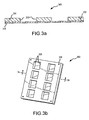
- Fig. 3a is a cross-sectional view of a middle structure comprising a flexible substrate and a support frame in accordance with one embodiment of the present invention
- Fig. 3b illustrates the middle structure of Fig. 3a from another perspective
- Fig. 4 is a cross-sectional view of the top plate, middle plate, and bottom plate of the assembly fixture in accordance with one embodiment of the present invention
- Fig. 5 is a cross-sectional view of the assembled fixture stretching the flexible substrate in accordance with one embodiment of the present invention
- Fig. 6 is a cross-sectional perspective of the assembled fixture of Fig. 5 ;
- Fig. 7 is a flow diagram illustrating a process of using the assembly fixture in accordance with one embodiment of the present invention.
- a component may have other ICs or components such as de-coupling capacitors that are required to complete the circuit. These components are typically assembled onto the component substrate prior to any molding or encapsulation process and typically utilize a solder paste process described above.
- solderable attachment pads or bumps are provided on the component to attach the component to another circuit board. These are often applied after the IC is bonded as described above. Therefore, solder bumps or other termination processing may occur after the IC is assembled. In addition, marking of the component to identify device number, part number, etc. may be required. Those steps are often performed prior to removing or singulating the component from the flex film strip. Finally, individual components are generally singulated into single units.
- the top plate and the bottom plate of the press are generally formed from material which has a low thermal mass.
- the material from which the top plate 100 and bottom plate 200 are formed from should be light and capable of surviving processing temperatures on the order of 300 degrees Celsius.
- materials from which the top plate 100 and bottom plate 200 can made primarily of include, but are not limited to, aluminum, titanium and Delmat.
- top plate 100 comprises a plurality of apertures 110.
- the openings 110 in the top plate allow for the placement of the ICs and other components for bonding to the substrate.
- the apertures 110 form rectangles which are aligned vertically and horizontally.
- the shape of the apertures need not be limited to rectangles.
- Other examples of aperture shapes include any other geometric shape or custom design.
- each aperture 110 on the top plate need not be the same shape.
- the apertures 110 are not aligned vertically and horizontally.
- each plate has screw holes, 120, 220, and 330, to aid in alignment of the structures and to help facilitate compressing the middle structure 300 between the top plate 100 and the bottom plate 200.
- other mechanisms and structures e.g. clamps may be used for the alignment and sandwiching of the plates.
- a die can be assembled by bonding one or more ICs to the flattened substrate through openings in the top carrier using flip chip technologies.
- the top plate, and the bottom plate are removed and the substrate and IC combination are cut away from the carrier by mechanical separation or through laser cutting process.
- the thin substrate ⁇ .001 inches
- the integrated circuit about .008 inches
- the solder used to bond the two together ⁇ .003 inches.
- the resulting packaged IC can be thinner than an IC constructed with conventional approaches.
- other components such as de-coupling capacitors, small resistors, or other ICs may be bonded in close proximity to the primary IC die to create a multi-chip device or module.
- embodiments relate to novel apparatus, methods and arrangements for assembling an IC die by flattening a flexible substrate.
Landscapes
- Wire Bonding (AREA)
Claims (27)
- Vorrichtung zum Glätten eines flexiblen Substrats, mit dem integrierte Schaltkreise kontaktiert werden können, welche Vorrichtung aufweist:eine obere Platte (100) mit mehreren Öffnungen (110);eine untere Platte (200) mit einem Netzwerk aus Kanälen (230), die zwischen sich erhabene Abschnitte (210) bilden, wobei die untere Platte (200) so angeordnet ist, dass jeder erhabene Abschnitt (210) einer Öffnung (110) in der oberen Platte (100) gegenüberliegt;eine mittlere Struktur (300) zwischen der oberen Platte (100) und der unteren Platte (200), wobei die mittlere Struktur (300) erhabene Abschnitte (320), die mit dem Netzwerk aus Kanälen (230), die sich auf der unteren Platte (200) befinden, in Eingriff bringbar sind, und Öffnungen, die den erhabenen Abschnitten (210) der unteren Platte (200) zugewandt sind, aufweist;ein flexibles Substrat (310), das sich zwischen der mittleren Struktur (300) und der unteren Platte (200) befindet;wodurch, wenn die obere Platte (100) auf die mittlere Struktur (300) zu der unteren Platte (200) hin heruntergedrückt wird, Teile des flexiblen Substrats (310) über den erhabenen Abschnitten (210) der unteren Platte (200) gestreckt werden.
- Vorrichtung nach Anspruch 1, bei der die obere Platte mehrere Öffnungen (110) hat, die horizontal und vertikal über die obere Platte angeordnet sind.
- Vorrichtung nach Anspruch 1, bei der die untere Platte (200) ein Netzwerk von Kanälen, die horizontale und vertikale Kanäle aufweisen, enthält.
- Vorrichtung nach Anspruch 1, bei der die erhabenen Abschnitte (320) der mittleren Struktur (300) horizontale und vertikale erhabene Abschnitte aufweisen, die mit den horizontalen und vertikalen Kanälen der unteren Platte ausgerichtet sind.
- Vorrichtung nach Anspruch 1, bei der jeder erhabene Abschnitt der unteren Platte einer Öffnung (110) der oberen Platte (100) zugewandt ist.
- Vorrichtung nach Anspruch 1, bei der das flexible Substrat (310) parallel zwischen dem mittleren Substrat (300) und der unteren Platte (200) angeordnet ist.
- Vorrichtung nach Anspruch 1, bei der die obere Platte (100) und die untere Platte (200) primär aus einem Material mit einer geringen thermischen Masse bestehen.
- Vorrichtung nach Anspruch 1, bei der die obere Platte (100) primär aus Aluminium besteht.
- Vorrichtung nach Anspruch 1, bei der das Netzwerk aus Kanälen (230), die erhabenen Abschnitte zwischen sich bilden, auf der unteren Platte vertikal und horizontal positioniert sind.
- Vorrichtung nach Anspruch 1, bei der das flexible Substrat (310) aus einem Material zusammengesetzt ist, das ausgewählt ist aus der Gruppe aufweisend Polyimid, Flüssigkristallpolymer (LCP) oder Polytetrafluorethylen (EPTFE).
- Vorrichtung nach Anspruch 1, bei der die Dicke des flexiblen Substrats (310) im Bereich von 0,5 mm bis 1 mm liegt.
- Vorrichtung nach Anspruch 1, bei der das Substrat (310) mehrere Schichten enthält.
- Vorrichtung nach Anspruch 1, bei der das Substrat (310) auf der Grundlage eines Satzes von Komponenten, die mit dem Substrat kontaktiert werden, maßgefertigt ist.
- Vorrichtung nach Anspruch 1, bei der eine Lücke durch eine flache Oberfläche der unteren Platte (200) gebildet ist.
- Vorrichtung nach Anspruch 1, bei der Abmessungen der erhabenen Bereiche der unteren Platte über die untere Platte (200) variieren.
- Vorrichtung nach Anspruch 1, bei der die Dicke der zusammengesetzten Vorrichtung im Bereich von 0,05 bis 1 Zoll liegt.
- Vorrichtung nach Anspruch 1, bei der die mittlere Struktur (300) einteilig mit dem Substrat ist, um einen Träger (320) für das Substrat (310) zu bilden.
- Vorrichtung nach Anspruch 17, bei der die Dicke des Trägers (320) für das Substrat im Bereich von 0,015 bis 0,125 Zoll liegt.
- Vorrichtung nach Anspruch 17, bei der der Träger (320) primär aus verstärktem Glaslaminat besteht.
- Vorrichtung nach Anspruch 19, bei der das verstärkte Glaslaminat FR4 ist.
- Verfahren zum Glätten eines flexiblen Substrats, mit dem integrierte Schaltkreise kontaktiert werden können, welches Verfahren aufweist:Ausrichten eines flexiblen Substrats (310) zwischen einem Rahmen (320) und einer unteren Platte (200), wobei die untere Platte (200) erhabene Abschnitte (210) mit Kanälen (230) dazwischen enthält, und wobei der Rahmen (320) Öffnungen enthält, die den erhabenen Abschnitten (210) der unteren Platte (200) zugewandt sind; undZusammendrücken des flexiblen Substrats (310) zwischen dem Rahmen (320) und der unteren Platte (200), derart, dass die Öffnungen des Rahmens und die erhabenen Abschnitte (210) der unteren Platte (200) ineinandergreifen, wodurch Teile des flexiblen Substrats (310) über den erhabenen Abschnitten (210) der unteren Platte (200) gestreckt werden.
- Verfahren nach Anspruch 21, bei dem das Zusammendrücken aufweist:Ausrichten einer oberen Platte (100) über dem Rahmen, wobei die obere Platte Öffnungen (110) hat, die mit den Öffnungen des Rahmens ausgerichtet sind; undHerunterdrücken der oberen Platte (100) auf den die Substratanordnung bildenden Rahmen (320).
- Verfahren nach Anspruch 21, weiterhin aufweisend:Aufbringen von Flussmittel oder eines leitenden Mediums auf das flexible Substrat durch zumindest eine Öffnung der oberen Platte (100);Anordnen von einer oder mehreren Komponentenvorrichtungen auf dem flexiblen Substrat (310) der Substratanordnung durch die zugeordnete, zumindest eine Öffnung der oberen Platte (100);Anbringen von Komponentenvorrichtungsanschlüssen auf gestreckten Bereichen des flexiblen Substrats (310) unter Verwendung von Lötmittel; undErwärmen der Substratanordnung mit angebrachten Komponentenvorrichtungen, um eine oder mehrere zusammengesetzte Komponenten zu bilden.
- Verfahren nach Anspruch 23, weiterhin aufweisend das Trennen der einen oder der mehreren zusammengesetzten Komponenten.
- Verfahren nach Anspruch 23, bei dem das leitende Medium eine Lötmittelpaste ist.
- Verfahren nach Anspruch 23, bei dem die Vorrichtungsanschlüsse nachfolgende Lötmittelbumps sind.
- Verfahren nach Anspruch 23, welches weiterhin aufweist:das Aufbringen einer Unterfüllungs- oder Überformungsverbindung; undHärten der Unterfüllungs- oder Überformungsverbindung.
Applications Claiming Priority (2)
| Application Number | Priority Date | Filing Date | Title |
|---|---|---|---|
| US11/166,461 US7226821B2 (en) | 2005-06-24 | 2005-06-24 | Flip chip die assembly using thin flexible substrates |
| PCT/US2006/024399 WO2007002346A1 (en) | 2005-06-24 | 2006-06-21 | Flip chip die assembly using thin flexible substrates |
Publications (2)
| Publication Number | Publication Date |
|---|---|
| EP1894239A1 EP1894239A1 (de) | 2008-03-05 |
| EP1894239B1 true EP1894239B1 (de) | 2012-08-01 |
Family
ID=37036984
Family Applications (1)
| Application Number | Title | Priority Date | Filing Date |
|---|---|---|---|
| EP06773810A Not-in-force EP1894239B1 (de) | 2005-06-24 | 2006-06-21 | Flip-Chipanordnung mit dünnen, flexiblen Substraten |
Country Status (4)
| Country | Link |
|---|---|
| US (2) | US7226821B2 (de) |
| EP (1) | EP1894239B1 (de) |
| JP (1) | JP5198265B2 (de) |
| WO (1) | WO2007002346A1 (de) |
Families Citing this family (13)
| Publication number | Priority date | Publication date | Assignee | Title |
|---|---|---|---|---|
| US7755162B2 (en) | 2004-05-06 | 2010-07-13 | Sidense Corp. | Anti-fuse memory cell |
| US9123572B2 (en) | 2004-05-06 | 2015-09-01 | Sidense Corporation | Anti-fuse memory cell |
| US8735297B2 (en) | 2004-05-06 | 2014-05-27 | Sidense Corporation | Reverse optical proximity correction method |
| SG153683A1 (en) * | 2007-12-14 | 2009-07-29 | Tezzaron Semiconductor S Pte L | 3d integrated circuit package and method of fabrication thereof |
| US20110147908A1 (en) * | 2009-12-17 | 2011-06-23 | Peng Sun | Module for Use in a Multi Package Assembly and a Method of Making the Module and the Multi Package Assembly |
| US9171794B2 (en) | 2012-10-09 | 2015-10-27 | Mc10, Inc. | Embedding thin chips in polymer |
| US8877558B2 (en) | 2013-02-07 | 2014-11-04 | Harris Corporation | Method for making electronic device with liquid crystal polymer and related devices |
| US9293438B2 (en) | 2013-07-03 | 2016-03-22 | Harris Corporation | Method for making electronic device with cover layer with openings and related devices |
| US9899330B2 (en) * | 2014-10-03 | 2018-02-20 | Mc10, Inc. | Flexible electronic circuits with embedded integrated circuit die |
| US10319619B2 (en) | 2014-12-05 | 2019-06-11 | Samsung Electronics Co., Ltd. | Equipment for manufacturing semiconductor devices and method for use of same for manufacturing semiconductor package components |
| WO2018125125A1 (en) * | 2016-12-29 | 2018-07-05 | Intel IP Corporation | Lead frame with angular deflections and wrapped printed wiring boards for system-in-package apparatus |
| WO2018125208A1 (en) * | 2016-12-30 | 2018-07-05 | Intel IP Corporation | Contoured-on-heat-sink, wrapped printed wiring boards for system-in-package apparatus |
| KR20220036952A (ko) * | 2019-07-12 | 2022-03-23 | 뉴럴링크 코포레이션 | 박막 전극 어레이 및 집적 회로를 위한 샌드위치 어셈블리 방식 |
Family Cites Families (31)
| Publication number | Priority date | Publication date | Assignee | Title |
|---|---|---|---|---|
| US4980219A (en) * | 1988-04-06 | 1990-12-25 | Casio Computer Co., Ltd. | Carrier tape for bonding IC devices and method of using the same |
| US5834339A (en) * | 1996-03-07 | 1998-11-10 | Tessera, Inc. | Methods for providing void-free layers for semiconductor assemblies |
| US5518964A (en) * | 1994-07-07 | 1996-05-21 | Tessera, Inc. | Microelectronic mounting with multiple lead deformation and bonding |
| US6273955B1 (en) * | 1995-08-28 | 2001-08-14 | Canon Kabushiki Kaisha | Film forming apparatus |
| JPH0992689A (ja) * | 1995-09-26 | 1997-04-04 | Shin Etsu Polymer Co Ltd | キャリアテープの製造方法 |
| US5760465A (en) * | 1996-02-01 | 1998-06-02 | International Business Machines Corporation | Electronic package with strain relief means |
| JPH09306948A (ja) * | 1996-05-10 | 1997-11-28 | Hitachi Ltd | インナリード・ボンディング方法および装置 |
| US6225688B1 (en) * | 1997-12-11 | 2001-05-01 | Tessera, Inc. | Stacked microelectronic assembly and method therefor |
| KR100251859B1 (ko) * | 1997-01-28 | 2000-04-15 | 마이클 디. 오브라이언 | 가요성 회로 기판 스트립을 이용하여 제조되는 볼그리드 어레이반도체 패키지의 싱귤레이션 방법 |
| US5919329A (en) * | 1997-10-14 | 1999-07-06 | Gore Enterprise Holdings, Inc. | Method for assembling an integrated circuit chip package having at least one semiconductor device |
| US6060341A (en) * | 1998-01-12 | 2000-05-09 | International Business Machines Corporation | Method of making an electronic package |
| JP3303825B2 (ja) | 1999-03-09 | 2002-07-22 | 日本電気株式会社 | 半導体装置の製造方法 |
| US6980017B1 (en) * | 1999-03-10 | 2005-12-27 | Micron Technology, Inc. | Test interconnect for bumped semiconductor components and method of fabrication |
| JP2002032031A (ja) * | 2000-05-12 | 2002-01-31 | Seiko Epson Corp | 電気光学装置の製造方法、端子の接続方法、電気光学装置および電子機器 |
| US7214566B1 (en) * | 2000-06-16 | 2007-05-08 | Micron Technology, Inc. | Semiconductor device package and method |
| JP3659133B2 (ja) | 2000-06-23 | 2005-06-15 | セイコーエプソン株式会社 | 半導体装置の製造方法 |
| DE10105164A1 (de) | 2000-11-06 | 2002-05-16 | Manfred Michalk | Verfahren und Vorrichtung zum Kontaktieren von Halbleiterchips |
| US20020110956A1 (en) * | 2000-12-19 | 2002-08-15 | Takashi Kumamoto | Chip lead frames |
| US6632704B2 (en) * | 2000-12-19 | 2003-10-14 | Intel Corporation | Molded flip chip package |
| US20020090749A1 (en) * | 2001-01-09 | 2002-07-11 | 3M Innovative Properties Company | Hermetic package for mems devices with integrated carrier |
| JP2003124256A (ja) | 2001-10-12 | 2003-04-25 | Matsushita Electric Ind Co Ltd | フレキシブル基板の実装方法 |
| SG115455A1 (en) * | 2002-03-04 | 2005-10-28 | Micron Technology Inc | Methods for assembly and packaging of flip chip configured dice with interposer |
| US6716754B2 (en) * | 2002-03-12 | 2004-04-06 | Micron Technology, Inc. | Methods of forming patterns and molds for semiconductor constructions |
| JP2003297879A (ja) | 2002-04-03 | 2003-10-17 | Sony Corp | 半導体チップ圧着装置 |
| JP2004039802A (ja) | 2002-07-02 | 2004-02-05 | Renesas Technology Corp | 半導体装置の製造方法および半導体製造装置 |
| US6665193B1 (en) * | 2002-07-09 | 2003-12-16 | Amerasia International Technology, Inc. | Electronic circuit construction, as for a wireless RF tag |
| US7061077B2 (en) * | 2002-08-30 | 2006-06-13 | Fairchild Semiconductor Corporation | Substrate based unmolded package including lead frame structure and semiconductor die |
| TW558913B (en) * | 2002-10-25 | 2003-10-21 | Ritdisplay Corp | OLED device, method of packaging OLED device and a machine of packaging OLED device |
| US6711312B1 (en) * | 2002-12-20 | 2004-03-23 | General Electric Company | Integrated optoelectronic circuit and method of fabricating the same |
| US7202179B2 (en) * | 2004-12-22 | 2007-04-10 | Hewlett-Packard Development Company, L.P. | Method of forming at least one thin film device |
| US7521313B2 (en) * | 2005-01-18 | 2009-04-21 | Hewlett-Packard Development Company, L.P. | Thin film device active matrix by pattern reversal process |
-
2005
- 2005-06-24 US US11/166,461 patent/US7226821B2/en not_active Expired - Fee Related
-
2006
- 2006-06-21 JP JP2008518412A patent/JP5198265B2/ja not_active Expired - Fee Related
- 2006-06-21 EP EP06773810A patent/EP1894239B1/de not_active Not-in-force
- 2006-06-21 WO PCT/US2006/024399 patent/WO2007002346A1/en not_active Ceased
- 2006-08-15 US US11/464,779 patent/US7497911B2/en not_active Expired - Fee Related
Also Published As
| Publication number | Publication date |
|---|---|
| US20060292756A1 (en) | 2006-12-28 |
| US7226821B2 (en) | 2007-06-05 |
| US20060290007A1 (en) | 2006-12-28 |
| JP2008544554A (ja) | 2008-12-04 |
| JP5198265B2 (ja) | 2013-05-15 |
| WO2007002346A1 (en) | 2007-01-04 |
| EP1894239A1 (de) | 2008-03-05 |
| US7497911B2 (en) | 2009-03-03 |
Similar Documents
| Publication | Publication Date | Title |
|---|---|---|
| US6066512A (en) | Semiconductor device, method of fabricating the same, and electronic apparatus | |
| US6770164B1 (en) | Method for attaching a semiconductor die to a substrate | |
| US8039309B2 (en) | Systems and methods for post-circuitization assembly | |
| US6701614B2 (en) | Method for making a build-up package of a semiconductor | |
| US20030227077A1 (en) | Microelectronic package having a bumpless laminated interconnection layer | |
| EP1894239B1 (de) | Flip-Chipanordnung mit dünnen, flexiblen Substraten | |
| JPWO1999035683A1 (ja) | 半導体装置及びその製造方法並びに電子機器 | |
| US7450395B2 (en) | Circuit module and circuit device including circuit module | |
| US8421204B2 (en) | Embedded semiconductor power modules and packages | |
| KR20000010668A (ko) | 성형된 유연 회로 볼 그리드 어레이 및 그 제조방법 | |
| US20100190294A1 (en) | Methods for controlling wafer and package warpage during assembly of very thin die | |
| JP2011171540A (ja) | モジュールの製造方法 | |
| JPH10173003A (ja) | 半導体装置とその製造方法およびフィルムキャリアテープとその製造方法 | |
| JPWO2018008066A1 (ja) | 転写方法および実装方法 | |
| TWI547217B (zh) | 微電子封裝體及用於製造微電子封裝體之方法 | |
| US7804179B2 (en) | Plastic ball grid array ruggedization | |
| CN108400218B (zh) | 一种基于csp型式的led封装方法 | |
| JP4038021B2 (ja) | 半導体装置の製造方法 | |
| CN100466209C (zh) | 半导体器件及其加工和封装方法 | |
| JPH04199723A (ja) | 半導体装置及び半導体装置の製造方法 | |
| US6645794B2 (en) | Method of manufacturing a semiconductor device by monolithically forming a sealing resin for sealing a chip and a reinforcing frame by transfer molding | |
| JP2003037125A (ja) | 回路装置の製造方法 | |
| US20060141666A1 (en) | Method for producing a module including an integrated circuit on a substrate and an integrated module manufactured thereby | |
| KR100666990B1 (ko) | Bga 패키지 및 그 제조방법 | |
| WO1999065076A1 (fr) | Dispositif a semiconducteur et procede de fabrication |
Legal Events
| Date | Code | Title | Description |
|---|---|---|---|
| PUAI | Public reference made under article 153(3) epc to a published international application that has entered the european phase |
Free format text: ORIGINAL CODE: 0009012 |
|
| 17P | Request for examination filed |
Effective date: 20071217 |
|
| AK | Designated contracting states |
Kind code of ref document: A1 Designated state(s): AT BE BG CH CY CZ DE DK EE ES FI FR GB GR HU IE IS IT LI LT LU LV MC NL PL PT RO SE SI SK TR |
|
| DAX | Request for extension of the european patent (deleted) | ||
| RIN1 | Information on inventor provided before grant (corrected) |
Inventor name: SMITH, DAVID, J. Inventor name: PRIMAVERA, ANTHONY, A. Inventor name: UNNIKRISHNAN, VIJESH |
|
| DAX | Request for extension of the european patent (deleted) | ||
| 17Q | First examination report despatched |
Effective date: 20091106 |
|
| GRAP | Despatch of communication of intention to grant a patent |
Free format text: ORIGINAL CODE: EPIDOSNIGR1 |
|
| RIC1 | Information provided on ipc code assigned before grant |
Ipc: H01L 21/48 20060101ALI20120113BHEP Ipc: H01L 23/498 20060101AFI20120113BHEP |
|
| RTI1 | Title (correction) |
Free format text: FLIP CHIP DIE ASSEMBLY USING THIN FLEXIBLE SUBSTRATES |
|
| GRAS | Grant fee paid |
Free format text: ORIGINAL CODE: EPIDOSNIGR3 |
|
| GRAA | (expected) grant |
Free format text: ORIGINAL CODE: 0009210 |
|
| AK | Designated contracting states |
Kind code of ref document: B1 Designated state(s): AT BE BG CH CY CZ DE DK EE ES FI FR GB GR HU IE IS IT LI LT LU LV MC NL PL PT RO SE SI SK TR |
|
| REG | Reference to a national code |
Ref country code: GB Ref legal event code: FG4D |
|
| REG | Reference to a national code |
Ref country code: CH Ref legal event code: EP Ref country code: AT Ref legal event code: REF Ref document number: 569060 Country of ref document: AT Kind code of ref document: T Effective date: 20120815 |
|
| REG | Reference to a national code |
Ref country code: IE Ref legal event code: FG4D |
|
| REG | Reference to a national code |
Ref country code: DE Ref legal event code: R096 Ref document number: 602006031124 Country of ref document: DE Effective date: 20120927 |
|
| REG | Reference to a national code |
Ref country code: NL Ref legal event code: VDEP Effective date: 20120801 |
|
| REG | Reference to a national code |
Ref country code: AT Ref legal event code: MK05 Ref document number: 569060 Country of ref document: AT Kind code of ref document: T Effective date: 20120801 |
|
| REG | Reference to a national code |
Ref country code: LT Ref legal event code: MG4D Effective date: 20120801 |
|
| PG25 | Lapsed in a contracting state [announced via postgrant information from national office to epo] |
Ref country code: IS Free format text: LAPSE BECAUSE OF FAILURE TO SUBMIT A TRANSLATION OF THE DESCRIPTION OR TO PAY THE FEE WITHIN THE PRESCRIBED TIME-LIMIT Effective date: 20121201 Ref country code: AT Free format text: LAPSE BECAUSE OF FAILURE TO SUBMIT A TRANSLATION OF THE DESCRIPTION OR TO PAY THE FEE WITHIN THE PRESCRIBED TIME-LIMIT Effective date: 20120801 Ref country code: CY Free format text: LAPSE BECAUSE OF FAILURE TO SUBMIT A TRANSLATION OF THE DESCRIPTION OR TO PAY THE FEE WITHIN THE PRESCRIBED TIME-LIMIT Effective date: 20120801 Ref country code: LT Free format text: LAPSE BECAUSE OF FAILURE TO SUBMIT A TRANSLATION OF THE DESCRIPTION OR TO PAY THE FEE WITHIN THE PRESCRIBED TIME-LIMIT Effective date: 20120801 Ref country code: FI Free format text: LAPSE BECAUSE OF FAILURE TO SUBMIT A TRANSLATION OF THE DESCRIPTION OR TO PAY THE FEE WITHIN THE PRESCRIBED TIME-LIMIT Effective date: 20120801 |
|
| PG25 | Lapsed in a contracting state [announced via postgrant information from national office to epo] |
Ref country code: SE Free format text: LAPSE BECAUSE OF FAILURE TO SUBMIT A TRANSLATION OF THE DESCRIPTION OR TO PAY THE FEE WITHIN THE PRESCRIBED TIME-LIMIT Effective date: 20120801 Ref country code: SI Free format text: LAPSE BECAUSE OF FAILURE TO SUBMIT A TRANSLATION OF THE DESCRIPTION OR TO PAY THE FEE WITHIN THE PRESCRIBED TIME-LIMIT Effective date: 20120801 Ref country code: GR Free format text: LAPSE BECAUSE OF FAILURE TO SUBMIT A TRANSLATION OF THE DESCRIPTION OR TO PAY THE FEE WITHIN THE PRESCRIBED TIME-LIMIT Effective date: 20121102 Ref country code: PL Free format text: LAPSE BECAUSE OF FAILURE TO SUBMIT A TRANSLATION OF THE DESCRIPTION OR TO PAY THE FEE WITHIN THE PRESCRIBED TIME-LIMIT Effective date: 20120801 Ref country code: BE Free format text: LAPSE BECAUSE OF FAILURE TO SUBMIT A TRANSLATION OF THE DESCRIPTION OR TO PAY THE FEE WITHIN THE PRESCRIBED TIME-LIMIT Effective date: 20120801 Ref country code: LV Free format text: LAPSE BECAUSE OF FAILURE TO SUBMIT A TRANSLATION OF THE DESCRIPTION OR TO PAY THE FEE WITHIN THE PRESCRIBED TIME-LIMIT Effective date: 20120801 Ref country code: PT Free format text: LAPSE BECAUSE OF FAILURE TO SUBMIT A TRANSLATION OF THE DESCRIPTION OR TO PAY THE FEE WITHIN THE PRESCRIBED TIME-LIMIT Effective date: 20121203 |
|
| PG25 | Lapsed in a contracting state [announced via postgrant information from national office to epo] |
Ref country code: NL Free format text: LAPSE BECAUSE OF FAILURE TO SUBMIT A TRANSLATION OF THE DESCRIPTION OR TO PAY THE FEE WITHIN THE PRESCRIBED TIME-LIMIT Effective date: 20120801 |
|
| PG25 | Lapsed in a contracting state [announced via postgrant information from national office to epo] |
Ref country code: DK Free format text: LAPSE BECAUSE OF FAILURE TO SUBMIT A TRANSLATION OF THE DESCRIPTION OR TO PAY THE FEE WITHIN THE PRESCRIBED TIME-LIMIT Effective date: 20120801 Ref country code: CZ Free format text: LAPSE BECAUSE OF FAILURE TO SUBMIT A TRANSLATION OF THE DESCRIPTION OR TO PAY THE FEE WITHIN THE PRESCRIBED TIME-LIMIT Effective date: 20120801 Ref country code: EE Free format text: LAPSE BECAUSE OF FAILURE TO SUBMIT A TRANSLATION OF THE DESCRIPTION OR TO PAY THE FEE WITHIN THE PRESCRIBED TIME-LIMIT Effective date: 20120801 Ref country code: RO Free format text: LAPSE BECAUSE OF FAILURE TO SUBMIT A TRANSLATION OF THE DESCRIPTION OR TO PAY THE FEE WITHIN THE PRESCRIBED TIME-LIMIT Effective date: 20120801 |
|
| PG25 | Lapsed in a contracting state [announced via postgrant information from national office to epo] |
Ref country code: SK Free format text: LAPSE BECAUSE OF FAILURE TO SUBMIT A TRANSLATION OF THE DESCRIPTION OR TO PAY THE FEE WITHIN THE PRESCRIBED TIME-LIMIT Effective date: 20120801 |
|
| PLBE | No opposition filed within time limit |
Free format text: ORIGINAL CODE: 0009261 |
|
| STAA | Information on the status of an ep patent application or granted ep patent |
Free format text: STATUS: NO OPPOSITION FILED WITHIN TIME LIMIT |
|
| 26N | No opposition filed |
Effective date: 20130503 |
|
| PG25 | Lapsed in a contracting state [announced via postgrant information from national office to epo] |
Ref country code: BG Free format text: LAPSE BECAUSE OF FAILURE TO SUBMIT A TRANSLATION OF THE DESCRIPTION OR TO PAY THE FEE WITHIN THE PRESCRIBED TIME-LIMIT Effective date: 20121101 |
|
| REG | Reference to a national code |
Ref country code: DE Ref legal event code: R097 Ref document number: 602006031124 Country of ref document: DE Effective date: 20130503 |
|
| PG25 | Lapsed in a contracting state [announced via postgrant information from national office to epo] |
Ref country code: ES Free format text: LAPSE BECAUSE OF FAILURE TO SUBMIT A TRANSLATION OF THE DESCRIPTION OR TO PAY THE FEE WITHIN THE PRESCRIBED TIME-LIMIT Effective date: 20121112 |
|
| PG25 | Lapsed in a contracting state [announced via postgrant information from national office to epo] |
Ref country code: MC Free format text: LAPSE BECAUSE OF FAILURE TO SUBMIT A TRANSLATION OF THE DESCRIPTION OR TO PAY THE FEE WITHIN THE PRESCRIBED TIME-LIMIT Effective date: 20120801 |
|
| REG | Reference to a national code |
Ref country code: CH Ref legal event code: PL |
|
| GBPC | Gb: european patent ceased through non-payment of renewal fee |
Effective date: 20130621 |
|
| REG | Reference to a national code |
Ref country code: IE Ref legal event code: MM4A |
|
| REG | Reference to a national code |
Ref country code: FR Ref legal event code: ST Effective date: 20140228 |
|
| REG | Reference to a national code |
Ref country code: DE Ref legal event code: R119 Ref document number: 602006031124 Country of ref document: DE Effective date: 20140101 |
|
| PG25 | Lapsed in a contracting state [announced via postgrant information from national office to epo] |
Ref country code: GB Free format text: LAPSE BECAUSE OF NON-PAYMENT OF DUE FEES Effective date: 20130621 Ref country code: CH Free format text: LAPSE BECAUSE OF NON-PAYMENT OF DUE FEES Effective date: 20130630 Ref country code: LI Free format text: LAPSE BECAUSE OF NON-PAYMENT OF DUE FEES Effective date: 20130630 Ref country code: DE Free format text: LAPSE BECAUSE OF NON-PAYMENT OF DUE FEES Effective date: 20140101 Ref country code: IE Free format text: LAPSE BECAUSE OF NON-PAYMENT OF DUE FEES Effective date: 20130621 |
|
| PG25 | Lapsed in a contracting state [announced via postgrant information from national office to epo] |
Ref country code: FR Free format text: LAPSE BECAUSE OF NON-PAYMENT OF DUE FEES Effective date: 20130701 Ref country code: IT Free format text: LAPSE BECAUSE OF NON-PAYMENT OF DUE FEES Effective date: 20130621 |
|
| PG25 | Lapsed in a contracting state [announced via postgrant information from national office to epo] |
Ref country code: TR Free format text: LAPSE BECAUSE OF FAILURE TO SUBMIT A TRANSLATION OF THE DESCRIPTION OR TO PAY THE FEE WITHIN THE PRESCRIBED TIME-LIMIT Effective date: 20120801 |
|
| PG25 | Lapsed in a contracting state [announced via postgrant information from national office to epo] |
Ref country code: HU Free format text: LAPSE BECAUSE OF FAILURE TO SUBMIT A TRANSLATION OF THE DESCRIPTION OR TO PAY THE FEE WITHIN THE PRESCRIBED TIME-LIMIT; INVALID AB INITIO Effective date: 20060621 Ref country code: LU Free format text: LAPSE BECAUSE OF NON-PAYMENT OF DUE FEES Effective date: 20130621 |