EP1894239B1 - Flip chip die assembly using thin flexible substrates - Google Patents
Flip chip die assembly using thin flexible substrates Download PDFInfo
- Publication number
- EP1894239B1 EP1894239B1 EP06773810A EP06773810A EP1894239B1 EP 1894239 B1 EP1894239 B1 EP 1894239B1 EP 06773810 A EP06773810 A EP 06773810A EP 06773810 A EP06773810 A EP 06773810A EP 1894239 B1 EP1894239 B1 EP 1894239B1
- Authority
- EP
- European Patent Office
- Prior art keywords
- bottom plate
- substrate
- top plate
- flexible substrate
- carrier
- Prior art date
- Legal status (The legal status is an assumption and is not a legal conclusion. Google has not performed a legal analysis and makes no representation as to the accuracy of the status listed.)
- Not-in-force
Links
Images


Classifications
-
- H—ELECTRICITY
- H01—ELECTRIC ELEMENTS
- H01L—SEMICONDUCTOR DEVICES NOT COVERED BY CLASS H10
- H01L21/00—Processes or apparatus adapted for the manufacture or treatment of semiconductor or solid state devices or of parts thereof
- H01L21/02—Manufacture or treatment of semiconductor devices or of parts thereof
- H01L21/04—Manufacture or treatment of semiconductor devices or of parts thereof the devices having at least one potential-jump barrier or surface barrier, e.g. PN junction, depletion layer or carrier concentration layer
- H01L21/48—Manufacture or treatment of parts, e.g. containers, prior to assembly of the devices, using processes not provided for in a single one of the subgroups H01L21/06 - H01L21/326
- H01L21/4814—Conductive parts
- H01L21/4846—Leads on or in insulating or insulated substrates, e.g. metallisation
-
- H—ELECTRICITY
- H01—ELECTRIC ELEMENTS
- H01L—SEMICONDUCTOR DEVICES NOT COVERED BY CLASS H10
- H01L23/00—Details of semiconductor or other solid state devices
- H01L23/48—Arrangements for conducting electric current to or from the solid state body in operation, e.g. leads, terminal arrangements ; Selection of materials therefor
- H01L23/488—Arrangements for conducting electric current to or from the solid state body in operation, e.g. leads, terminal arrangements ; Selection of materials therefor consisting of soldered or bonded constructions
- H01L23/498—Leads, i.e. metallisations or lead-frames on insulating substrates, e.g. chip carriers
- H01L23/4985—Flexible insulating substrates
-
- H—ELECTRICITY
- H01—ELECTRIC ELEMENTS
- H01L—SEMICONDUCTOR DEVICES NOT COVERED BY CLASS H10
- H01L23/00—Details of semiconductor or other solid state devices
- H01L23/52—Arrangements for conducting electric current within the device in operation from one component to another, i.e. interconnections, e.g. wires, lead frames
- H01L23/538—Arrangements for conducting electric current within the device in operation from one component to another, i.e. interconnections, e.g. wires, lead frames the interconnection structure between a plurality of semiconductor chips being formed on, or in, insulating substrates
- H01L23/5387—Flexible insulating substrates
-
- H—ELECTRICITY
- H01—ELECTRIC ELEMENTS
- H01L—SEMICONDUCTOR DEVICES NOT COVERED BY CLASS H10
- H01L2924/00—Indexing scheme for arrangements or methods for connecting or disconnecting semiconductor or solid-state bodies as covered by H01L24/00
- H01L2924/0001—Technical content checked by a classifier
- H01L2924/0002—Not covered by any one of groups H01L24/00, H01L24/00 and H01L2224/00
Definitions
- Various embodiments of the present invention generally relate to apparatus and methods for assembling flip chip dies with thin flexible substrates. More specifically, embodiments relate to apparatus and methods flattening thin substrate surfaces by stretching thin flexible substrates to which ICs can be bonded.
- CMOS complementary metal-oxide-semiconductor
- IC integrated circuits
- CMOS complementary metal-oxide-semiconductor
- a flip chip assembly forms a direct electrical connection between an electronic component and a substrate, circuit board, or carrier, by means of conductive bumps on chip bond pads of the electronic component.
- the flip chip die is assembled by stretching thin flexible substrates to which ICs can be bonded. Stretching can be performed using embodiments of a top plate and bottom plate, with the flexible substrate disposed therebetween. Compressing the flexible substrate between the top plate and the bottom plate stretches portions of the flexible substrate over the raised sections of the bottom plate.
- the top plate and bottom plate are positioned such that each raised section of the bottom plate is opposite an aperture of the top plate.
- the middle plate is positioned between the top and the bottom plate in manner such that the carrier portions are above the network of channels created by the raised sections of the bottom plate.
- the top plate is then pressed down on the middle structure toward the bottom plate resulting in portions of the substrate to stretch over the raised sections of the bottom plate.
- Fig. 1a is a plan view of a top plate in accordance with one embodiment of the present invention.
- Fig. 1 b illustrates the top plate of Fig. 1 a from another perspective
- Fig. 2a is a plan view of a bottom plate in accordance with one embodiment of the present invention.
- Fig. 2b illustrates the bottom plate of Fig. 2a from another perspective
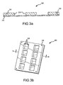
- Fig. 3a is a cross-sectional view of a middle structure comprising a flexible substrate and a support frame in accordance with one embodiment of the present invention
- Fig. 3b illustrates the middle structure of Fig. 3a from another perspective
- Fig. 4 is a cross-sectional view of the top plate, middle plate, and bottom plate of the assembly fixture in accordance with one embodiment of the present invention
- Fig. 5 is a cross-sectional view of the assembled fixture stretching the flexible substrate in accordance with one embodiment of the present invention
- Fig. 6 is a cross-sectional perspective of the assembled fixture of Fig. 5 ;
- Fig. 7 is a flow diagram illustrating a process of using the assembly fixture in accordance with one embodiment of the present invention.
- a component may have other ICs or components such as de-coupling capacitors that are required to complete the circuit. These components are typically assembled onto the component substrate prior to any molding or encapsulation process and typically utilize a solder paste process described above.
- solderable attachment pads or bumps are provided on the component to attach the component to another circuit board. These are often applied after the IC is bonded as described above. Therefore, solder bumps or other termination processing may occur after the IC is assembled. In addition, marking of the component to identify device number, part number, etc. may be required. Those steps are often performed prior to removing or singulating the component from the flex film strip. Finally, individual components are generally singulated into single units.
- the top plate and the bottom plate of the press are generally formed from material which has a low thermal mass.
- the material from which the top plate 100 and bottom plate 200 are formed from should be light and capable of surviving processing temperatures on the order of 300 degrees Celsius.
- materials from which the top plate 100 and bottom plate 200 can made primarily of include, but are not limited to, aluminum, titanium and Delmat.
- top plate 100 comprises a plurality of apertures 110.
- the openings 110 in the top plate allow for the placement of the ICs and other components for bonding to the substrate.
- the apertures 110 form rectangles which are aligned vertically and horizontally.
- the shape of the apertures need not be limited to rectangles.
- Other examples of aperture shapes include any other geometric shape or custom design.
- each aperture 110 on the top plate need not be the same shape.
- the apertures 110 are not aligned vertically and horizontally.
- each plate has screw holes, 120, 220, and 330, to aid in alignment of the structures and to help facilitate compressing the middle structure 300 between the top plate 100 and the bottom plate 200.
- other mechanisms and structures e.g. clamps may be used for the alignment and sandwiching of the plates.
- a die can be assembled by bonding one or more ICs to the flattened substrate through openings in the top carrier using flip chip technologies.
- the top plate, and the bottom plate are removed and the substrate and IC combination are cut away from the carrier by mechanical separation or through laser cutting process.
- the thin substrate ⁇ .001 inches
- the integrated circuit about .008 inches
- the solder used to bond the two together ⁇ .003 inches.
- the resulting packaged IC can be thinner than an IC constructed with conventional approaches.
- other components such as de-coupling capacitors, small resistors, or other ICs may be bonded in close proximity to the primary IC die to create a multi-chip device or module.
- embodiments relate to novel apparatus, methods and arrangements for assembling an IC die by flattening a flexible substrate.
Abstract
Description
- Various embodiments of the present invention generally relate to apparatus and methods for assembling flip chip dies with thin flexible substrates. More specifically, embodiments relate to apparatus and methods flattening thin substrate surfaces by stretching thin flexible substrates to which ICs can be bonded.
- Traditionally, three approaches have been employed for connecting integrated circuits (ICs) to printed circuit boards. These approaches are wire bonding, chip carriers with beam leads, and direct chip connections. Flip chip technology is one of the direct chip connection approaches. In general, a flip chip assembly forms a direct electrical connection between an electronic component and a substrate, circuit board, or carrier, by means of conductive bumps on chip bond pads of the electronic component.
- Flip chip technology has been used since the early 1960's. Compared to other packaging methods, flip chip technology provides increased performance in several areas, such as smaller package sizes, increased performance in high frequency applications, improved thermal capabilities, more I/O connections on a smaller die, and increased reliability. With these advantages, flip chip technology has found applications in the computer industry, automotive applications, electronic watches, cellular phones, pagers, and the like.
- There is a constant push in the industry to achieve smaller die packages. Unfortunately, traditional flip chip assembly techniques have characteristics that limit the minimum thickness that can be achieved. One problem relates to the common use of the relatively thick, rigid polymer substrates. With the current technologies, by bonding of the silicon ICs to a rigid polymer substrate, devices currently in commercial production are on the order of 1 millimeter (mm) in thickness.
- Flexible polymer substrates have been used in some approaches. However, previous direct chip connection approaches using thin flexible polymer substrates have typically been unsuccessful. One problem relates to uneven surfaces common to flexible polymer substrates. Such flexible substrates do not have the proper flatness for accurately bonding ICs using surface mount technologies (e.g., flip chip) with traditional approaches to die assembly. Because the polymers are so thin, it is difficult to manufacture polymers having sufficiently flat surfaces.
- One solution to the problem is disclosed in
US 6,080,603 , where an essentially flat polymer surface is bonded with a microelectronic element by placing the microelectronic element on a rigid surface, placing the polymer substrate on top of the microelectronic element and pushing upon the surface with an added disk to achieve bonding between the microelectronic element and the flexible substrate. Yet this method does not allow to produce substrates which are flattened before the microelectronic elements are bonded to the flexible substrate. - Hence, there exists a need in the art for apparatus and methods for flattening the thin flexible substrates to facilitate accurate bonding of ICs with the substrate.
- Various embodiments of the present invention include apparatus and methods for assembling flip chip dies including thin substrate surfaces. In some embodiments, the flip chip die is assembled by stretching thin flexible substrates to which ICs can be bonded. Stretching can be performed using embodiments of a top plate and bottom plate, with the flexible substrate disposed therebetween. Compressing the flexible substrate between the top plate and the bottom plate stretches portions of the flexible substrate over the raised sections of the bottom plate.
- In a particular embodiment of an apparatus, the top plate and bottom plate are positioned such that each raised section of the bottom plate is opposite an aperture of the top plate. The middle plate is positioned between the top and the bottom plate in manner such that the carrier portions are above the network of channels created by the raised sections of the bottom plate. The top plate is then pressed down on the middle structure toward the bottom plate resulting in portions of the substrate to stretch over the raised sections of the bottom plate.
- A more complete understanding may be derived by referring to the detailed description of preferred embodiments and claims when considered in connection with the figures.
- While multiple embodiments are disclosed, still other embodiments of the present invention will become apparent to those skilled in the art from the following detailed description, which shows and describes illustrative embodiments of the invention.
- In the Figures, similar components and/or features may have the same reference label. Further, various components of the same type may be distinguished by following the reference label with a second label that distinguishes among the similar components. If only the first reference label is used in the specification, the description is applicable to any one of the similar components having the same first reference label irrespective of the second reference label.
-
Fig. 1a is a plan view of a top plate in accordance with one embodiment of the present invention; -
Fig. 1 b illustrates the top plate ofFig. 1 a from another perspective; -
Fig. 2a is a plan view of a bottom plate in accordance with one embodiment of the present invention; -
Fig. 2b illustrates the bottom plate ofFig. 2a from another perspective; -
Fig. 3a is a cross-sectional view of a middle structure comprising a flexible substrate and a support frame in accordance with one embodiment of the present invention; -
Fig. 3b illustrates the middle structure ofFig. 3a from another perspective; -
Fig. 4 is a cross-sectional view of the top plate, middle plate, and bottom plate of the assembly fixture in accordance with one embodiment of the present invention; -
Fig. 5 is a cross-sectional view of the assembled fixture stretching the flexible substrate in accordance with one embodiment of the present invention; -
Fig. 6 is a cross-sectional perspective of the assembled fixture ofFig. 5 ; and -
Fig. 7 is a flow diagram illustrating a process of using the assembly fixture in accordance with one embodiment of the present invention. - While the invention is amenable to various modifications and alternative forms, specific embodiments have been shown by way of example in the drawings and are described in detail below. The intention, however, is not to limit the invention to the particular embodiments described. On the contrary, the invention is intended to cover all modifications, equivalents, and alternatives falling within the scope of the invention as defined by the appended claims.
- Apparatus and methods are described for creating thin substrate surfaces by flattening thin flexible substrates to which ICs can be bonded. Embodiments presented below generally facilitate the manufacture of thinner integrated circuits (ICs) by flatting thin flexible substrates to create a die assembly. ICs can be accurately bonded to the flattened substrate using direct connection technologies, such as surface mount (e.g., flip chip).
- According to one embodiment, the flip chip assembly process generally comprises one or more of the following: (1) fabrication of the component or chip substrate; (2) fabrication of a bumped IC wafer; (3) singulation of the die from the wafer; (4) picking and inspection of die from a die feeder; (5)fluxing the die or carrier site by dipping, transfer, spray, dispensing, or brushing methods; (6)placement of the die onto the fluxed site; (7) fusing of the solder bumps to the attachment pads by reflow soldering; (8) post reflow underfill (e.g., epoxy dispensing); (9) epoxy cure; (10) solder bump attachment; (11) singulation (i.e., the cutting of a wafer into individual die); and (12) test and final processing.
- In general, there are several steps typically performed to fabricate a semiconductor component. At a high level, various embodiments relate to the interconnection of the terminations on the IC with the remaining devices on the circuit board. Typically, the IC termination pads are very small and the spacing (pitch) between conducting pads is equally small. This makes direct connection to the circuit board more challenging. In addition, testing and burn in of the IC is difficult in the raw IC format and thus requires the die to be packaged in a housing of reasonable size etc. to allow testing in sockets or probe stations. Therefore, a component package is useful not only to house the IC but to allow a more robust test configuration and a larger termination pitch for easy assembly.
- There are several methods to interconnect the IC with the circuit board. One way is to package the IC in an organic container (component body). The component will house the IC, protect it and allow for proper testing etc. The first level connection (between the IC and component) can be accomplished in several ways including wirebond, ribbon bond, conductive adhesives and soldering. In the soldering case, for example, the IC has solderable termination pads, onto which solder is deposited at the IC fabricator. To join the IC solder bumps with corresponding attachment pads on a conductive layer in our component a flexible film with copper circuits and attachment pads in our prototypes may be used. The flex film has a circuit pattern that allows the IC bumps to align with the component film pads.
- Flux is most often utilized to clean the attachment pads and the IC bumps prior to solder joining. The flux is a resin most often made of pine tree sap (acidic) that when heated removes all oxides on the metal conductive surfaces and allows for a proper melting of the solder to occur. The flux is deposited onto the attachment pads on the flex film directly (for example fluid dispense, pin transfer, or jetting) or it can be applied the bumps on the IC by dipping the IC into a flux film. A solder paste (flux plus solder particles) may also be used to join the IC pads and circuit pads on the component. Once the flux or paste is applied, the IC is brought into contact with the component by alignment of the IC bumps and component pads in a placement machine.
- The reflow process generally involves heating the assembly in a controlled profile (time and temperature) until the flux activates, oxides are removed, and the solder is melted. Once melted, the solder joins with the attachment pad surface and makes a metallurgical bond. Upon cooling, the solder solidifies and the solder interconnection is complete. Often the IC is further protected by deposition of an encapsulating material either over or in between the IC and component surface. The encapsulation process can be achieved by dispensing or jetting a liquid epoxy or by over-mold injection. Once the resin is cured, it protects the IC and component's fragile circuitry.
- In addition to the primary IC, a component may have other ICs or components such as de-coupling capacitors that are required to complete the circuit. These components are typically assembled onto the component substrate prior to any molding or encapsulation process and typically utilize a solder paste process described above.
- Once the component has the IC and subsequent components attached to the substrate, other features may be required to complete the functional or aesthetic aspects of the device. For example, once finished, the component will be ultimately used in building an electronic device or apparatus of some kind. Typically solderable attachment pads or bumps are provided on the component to attach the component to another circuit board. These are often applied after the IC is bonded as described above. Therefore, solder bumps or other termination processing may occur after the IC is assembled. In addition, marking of the component to identify device number, part number, etc. may be required. Those steps are often performed prior to removing or singulating the component from the flex film strip. Finally, individual components are generally singulated into single units.
- Embodiments described herein beneficially maintain the substrate flatness during the assembly process through singulation. According to one embodiment, the use of a window frame type component carrier allows circuit board manufacturers to process thin laminates and flex films through their manufacturing processes. The flex film is bonded to a rigid carrier. The carrier is placed into a specialized fixture. A bottom pallet with raised regions is created that allows the windowed region of the flex film to be pressed flat. A top portion of the carrier is joined to the bottom part of the carrier such that the windowed region of the flex film is stretched (e.g., like a drum or knitting hoop). The die assembly site is held flat overtop of the raised portion of the carrier to provide a stable vase for placement of the die. The carrier retains the flex board stability during subsequent reflow processes.
- Terminology
- Brief definitions of terms and/or phrases used throughout this application are given below. The terms "connected" or "coupled" and related terms are used in an operational sense and are not necessarily limited to a direct connection or coupling. Thus, for example, two devices may be coupled directly, or via one or more devices. Based on the disclosure provided herein, one of ordinary skill in the art will appreciate a variety of ways in which connection or coupling exists in accordance with the aforementioned definition.
- The phrases "in one embodiment," "according to one embodiment," and the like generally means the particular feature, structure, or characteristic following the phrase is included in at least one embodiment of the present invention, and may be included in more than one embodiment of the present invention. Importantly, such phrases do not necessarily refer to the same embodiment.
- If the specification states a component or feature "may," "can," "could," or "might" be included or have a characteristic, property, or structure, that particular component or feature is not required to be included or have the characteristic, property, or structure.
- According to some embodiments of the invention, a thin polymer substrate is first bonded to a carrier plate. The thin polymer substrate can be a polymer, such as, but not limited to, Kapton-polyimide, liquid crystal polymer (LCP), or EPTFE and can be about .0005 to 0.005 inches thick. The carrier is typically a rigid polymer substrate, such as FR4, and is about .015 to 0.125 inches thick. To flatten out the thin polymer, a press can be used, which includes a top plate and a bottom plate.
- The top plate and the bottom plate of the press are generally formed from material which has a low thermal mass. In addition, the material from which the
top plate 100 andbottom plate 200 are formed from should be light and capable of surviving processing temperatures on the order of 300 degrees Celsius. Thus, as just some examples, materials from which thetop plate 100 andbottom plate 200 can made primarily of include, but are not limited to, aluminum, titanium and Delmat. - Referring now to
Figs. 1a-1b , one embodiment oftop plate 100 in accordance with the present invention is shown. In the illustrated embodiment,top plate 100 comprises a plurality ofapertures 110. Theopenings 110 in the top plate allow for the placement of the ICs and other components for bonding to the substrate. In the embodiment depicted, theapertures 110 form rectangles which are aligned vertically and horizontally. In other embodiments, the shape of the apertures need not be limited to rectangles. Other examples of aperture shapes include any other geometric shape or custom design. Furthermore, eachaperture 110 on the top plate need not be the same shape. In yet other embodiments, theapertures 110 are not aligned vertically and horizontally. - One embodiment of the
bottom plate 200 is depicted inFigs. 2a-2b . The bottom plate includes raisedregions 210. The raisedregions 210 are positioned such that each raised section is aligned with anopening 110 of the top plate. Between the raised regions 210 a network ofchannels 230 is formed. In the illustrated embodiment, the raisedsections 210 are rectangles which are aligned vertically and horizontally. The shape of the raisedsection 210, however, is not limited to rectangles aligned vertically and horizontally. Typically, the shape and placement of the raisedsections 210 should be similar in design and placement as theopenings 110 in the top plate. -
Figs. 3a-3b provide views of one embodiment of themiddle structure 300. A thinflexible substrate 310 is mounted to a carrier, or support frame, 320. Thecarrier 320 forms a raised section capable of meshing with the network ofchannels 230 located on thebottom plate 200. The circuit pattern or design on the flexible substrate depends on the IC design. In this particular embodiment, the thickness of theflexible substrate 310 ranges from 0.0005 to 0.005 inches and may contain multiple layers depending on the design. Examples of primary substrate materials include, but are not limited to, polyimide, liquid crystal polymer and polytetraflouroethylene (EPTFE). Thecarrier 320 typically has a thickness in the range of 0.015 to 0.125 inches. The carrier is typically, but not necessarily, composed of a cheaper material such as a reinforced glass laminate (e.g. FR4). -
Fig. 4 illustrates how thetop plate 100,bottom plate 200, and themiddle structure 300 can be aligned in accordance with one embodiment. Thetop plate 100,bottom plate 200, andmiddle structure 300 are positioned substantially parallel to each other, with the middle structure between thetop plate 100 andbottom plate 200. Theopenings 110 of thetop plate 100 are aligned overtop of the raisedportions 210 of thebottom plate 200. Thesupport frame 320 is aligned with the network ofchannels 230 of thebottom plate 200, such that when thetop plate 100 is pressed down toward thebottom plate 200, thesupport frame 320 meshes with the network ofchannels 230. - In accordance with the particular embodiment illustrated in
Figs. 5-6 , the flex film substrate and carrier are sandwiched between totop plate 100 andbottom plate 200. By pressing the plates together, the raised regions of thebottom plate 200 push the flex film substrate upward and around the carrier. By pressing the thin substrate upward, the substrate is stretched like a drum head, thereby flattening thesubstrate 310. In the embodiments depicted inFigs. 1-4 , each plate has screw holes, 120, 220, and 330, to aid in alignment of the structures and to help facilitate compressing themiddle structure 300 between thetop plate 100 and thebottom plate 200. In other embodiments, other mechanisms and structures (e.g. clamps) may be used for the alignment and sandwiching of the plates. - Having described an exemplary assembly apparatus, a block diagram 700 representing a high level overview of the use according to one embodiment of the present invention will now be described with reference to
Fig. 7 . Atstep 710, the middle fixture and substrate are placed over the bottom plate in such a manner that the network of channels in the bottom plate are aligned with the support frame of the middle structure. On top of the middle structure the top plate is aligned in a manner that the openings of the top plate are positioned over the raised sections of the bottom plate atstep 720. The substrate is compressed between the top and bottom plate atstep 730 causing the substrate to stretch across the raised portions of the bottom plate. - After the flexible substrate is stretched, a die can be assembled by bonding one or more ICs to the flattened substrate through openings in the top carrier using flip chip technologies. In some embodiments, after the ICs are bonded to the thin substrate, the top plate, and the bottom plate are removed and the substrate and IC combination are cut away from the carrier by mechanical separation or through laser cutting process. Thus, all that remains is the thin substrate (< .001 inches), the integrated circuit (about .008 inches), and the solder used to bond the two together (< .003 inches). The resulting packaged IC can be thinner than an IC constructed with conventional approaches. Additionally, other components such as de-coupling capacitors, small resistors, or other ICs may be bonded in close proximity to the primary IC die to create a multi-chip device or module.
- In conclusion, embodiments relate to novel apparatus, methods and arrangements for assembling an IC die by flattening a flexible substrate.
Claims (27)
- An apparatus for flattening a flexible substrate to which integrated circuits can be bonded, the apparatus comprising:a top plate (100) having a plurality of apertures (110);a bottom plate (200) having a network of channels (230) forming raised sections (210) therebetween, the bottom plate (200) positioned such that each raised section (210) is opposite an aperture (110) of the top plate (100);a middle structure (300) between the top plate (100) and the bottom plate (200), the middle structure (300) comprising raised sections (320) meshing with the network of channels (230) located on the bottom plate (200) and openings facing the raised sections (210) of the bottom plate (200);a flexible substrate (310) disposed between the middle structure (300) and the bottom plate (200);whereby when the top plate (100) is pressed down on the middle structure (300) toward the bottom plate (200), portions of the flexible substrate (310) stretch over the raised sections (210) of the bottom plate (200).
- The apparatus of claim 1, wherein the top plate has a plurality of apertures (110) that are positioned horizontally and vertically around the top plate.
- The apparatus of claim 1, wherein the bottom plate (200) includes a network of channels comprises horizontal and vertical channels.
- The apparatus of claim 1, wherein the raised sections (320) of the middle structure (300) comprise horizontal and vertical raised sections that are aligned with the horizontal and vertical channels of the bottom plate.
- The apparatus of claim 1, wherein each raised section of the bottom plate faces an aperture (110) of the top plate (100).
- The apparatus of claim 1, wherein the flexible substrate (310) is paralleledly disposed between the middle substrate (300) and the bottom plate (200).
- The apparatus of claim 1, wherein the top plate (100) and the bottom plate (200) are primarily comprised of a material with a low thermal mass.
- The apparatus of claim 1, wherein the top plate (100) is comprised primarily of aluminum.
- The apparatus of claim 1, wherein the network of channels (230) forming raised sections therebetween are vertically and horizontally positioned on the bottom plate.
- The apparatus of claim 1, wherein the flexible substrate (310) is composed of a material selected from a group comprising: polyimide, liquid crystal polymer (LCP), or polytetrafluoroethylene (EPTFE).
- The apparatus of claim 1, wherein the thickness of the flexible substrate (310) ranges from .5 mm to 1 mm.
- The apparatus of claim 1, wherein the substrate (310) contains multiple layers.
- The apparatus of claim 1, wherein the substrate (310) contains a custom design based on a set of components which will be bonded to the substrate.
- The apparatus of claim 1, wherein a void is formed by a flat surface of the bottom plate (200).
- The apparatus of claim 1, wherein dimensions of the raised portions of the bottom plate varies across the bottom plate (200).
- The apparatus of claim 1, wherein the thickness of the assembled fixture ranges from 0.05 to 1 inches.
- The apparatus of claim 1, wherein the middle structure (300) is integrated with the substrate to form a carrier (320) for the substrate (310).
- The apparatus of claim 17, wherein the thickness of the carrier (320) for the substrate ranges from 0.015 to 0.125 inches.
- The apparatus of claim 17, wherein the carrier (320) is primarily composed of reinforced glass laminate.
- The apparatus of claim 19, wherein the reinforced glass laminate is FR4.
- A method for flattening a flexible substrate to which integrated circuits can be bonded, the method comprising:aligning a flexible substrate (310) between a frame (320) and a bottom plate (200), wherein the bottom plate (200) includes raised sections (210) having channels (230) therebetween, and wherein the frame (320) includes openings facing the raised sections (210) of the bottom plate (200); andcompressing the flexible substrate (310) between the frame (320) and the bottom plate (200), such that the openings of the frame mesh with the raised sections (210) of the bottom plate (200), thereby stretching portions of the flexible substrate (310) across the raised sections (210) of the bottom plate (200).
- The method of claim 21, wherein compressing comprises:aligning a top plate (100) above the frame, the top plate having openings (110) aligned with the openings of the frame; andpressing the top plate (100) down upon the frame (320) forming a substrate assembly.
- The method of claim 21 further comprising:depositing flux or a conductive media on the flexible substrate through at least one opening of the top plate (100);placing one or more component devices on the flexible substrate (310) of the substrate assembly through the associated at least one opening of the top plate (100);attaching component device terminations to stretched portions of the flexible substrate (310) using solder; andheating the substrate assembly with attached component devices to form one or more assembled components.
- The method of claim 23, further comprising separating the one or more assembled components.
- The method of claim 23, wherein the conductive media is a solder paste.
- The method of claim 23, wherein the device terminations are subsequent solder bumps.
- The method of claim 23, further comprising:the deposition of an underfill or overmold compounds; andcuring of said underfill or overmold compounds.
Applications Claiming Priority (2)
| Application Number | Priority Date | Filing Date | Title |
|---|---|---|---|
| US11/166,461 US7226821B2 (en) | 2005-06-24 | 2005-06-24 | Flip chip die assembly using thin flexible substrates |
| PCT/US2006/024399 WO2007002346A1 (en) | 2005-06-24 | 2006-06-21 | Flip chip die assembly using thin flexible substrates |
Publications (2)
| Publication Number | Publication Date |
|---|---|
| EP1894239A1 EP1894239A1 (en) | 2008-03-05 |
| EP1894239B1 true EP1894239B1 (en) | 2012-08-01 |
Family
ID=37036984
Family Applications (1)
| Application Number | Title | Priority Date | Filing Date |
|---|---|---|---|
| EP06773810A Not-in-force EP1894239B1 (en) | 2005-06-24 | 2006-06-21 | Flip chip die assembly using thin flexible substrates |
Country Status (4)
| Country | Link |
|---|---|
| US (2) | US7226821B2 (en) |
| EP (1) | EP1894239B1 (en) |
| JP (1) | JP5198265B2 (en) |
| WO (1) | WO2007002346A1 (en) |
Families Citing this family (13)
| Publication number | Priority date | Publication date | Assignee | Title |
|---|---|---|---|---|
| US9123572B2 (en) | 2004-05-06 | 2015-09-01 | Sidense Corporation | Anti-fuse memory cell |
| US8735297B2 (en) | 2004-05-06 | 2014-05-27 | Sidense Corporation | Reverse optical proximity correction method |
| US7755162B2 (en) | 2004-05-06 | 2010-07-13 | Sidense Corp. | Anti-fuse memory cell |
| SG153683A1 (en) * | 2007-12-14 | 2009-07-29 | Tezzaron Semiconductor S Pte L | 3d integrated circuit package and method of fabrication thereof |
| US20110147908A1 (en) * | 2009-12-17 | 2011-06-23 | Peng Sun | Module for Use in a Multi Package Assembly and a Method of Making the Module and the Multi Package Assembly |
| US9171794B2 (en) | 2012-10-09 | 2015-10-27 | Mc10, Inc. | Embedding thin chips in polymer |
| US8877558B2 (en) | 2013-02-07 | 2014-11-04 | Harris Corporation | Method for making electronic device with liquid crystal polymer and related devices |
| US9293438B2 (en) | 2013-07-03 | 2016-03-22 | Harris Corporation | Method for making electronic device with cover layer with openings and related devices |
| US9899330B2 (en) * | 2014-10-03 | 2018-02-20 | Mc10, Inc. | Flexible electronic circuits with embedded integrated circuit die |
| CN107004671B (en) * | 2014-12-05 | 2019-11-19 | 三星电子株式会社 | The method for manufacturing the equipment of semiconductor device and manufacturing semiconductor package part using it |
| US11145577B2 (en) | 2016-12-29 | 2021-10-12 | Intel Corporation | Lead frame with angular deflections and wrapped printed wiring boards for system-in-package apparatus |
| US11037855B2 (en) * | 2016-12-30 | 2021-06-15 | Intel IP Corporation | Contoured-on-heat-sink, wrapped printed wiring boards for system-in-package apparatus |
| US11444056B2 (en) | 2019-07-12 | 2022-09-13 | Neuralink Corp. | Sandwich assembly scheme for thin film electrode array and integrated circuits on both sides of printed circuit board (PCB) and method of manufacture |
Family Cites Families (31)
| Publication number | Priority date | Publication date | Assignee | Title |
|---|---|---|---|---|
| US4980219A (en) | 1988-04-06 | 1990-12-25 | Casio Computer Co., Ltd. | Carrier tape for bonding IC devices and method of using the same |
| US5834339A (en) | 1996-03-07 | 1998-11-10 | Tessera, Inc. | Methods for providing void-free layers for semiconductor assemblies |
| US5518964A (en) * | 1994-07-07 | 1996-05-21 | Tessera, Inc. | Microelectronic mounting with multiple lead deformation and bonding |
| US6273955B1 (en) * | 1995-08-28 | 2001-08-14 | Canon Kabushiki Kaisha | Film forming apparatus |
| JPH0992689A (en) * | 1995-09-26 | 1997-04-04 | Shin Etsu Polymer Co Ltd | Manufacture of carrier tape |
| US5760465A (en) * | 1996-02-01 | 1998-06-02 | International Business Machines Corporation | Electronic package with strain relief means |
| JPH09306948A (en) * | 1996-05-10 | 1997-11-28 | Hitachi Ltd | Method and apparatus for bonding inner leads |
| US6225688B1 (en) | 1997-12-11 | 2001-05-01 | Tessera, Inc. | Stacked microelectronic assembly and method therefor |
| KR100251859B1 (en) | 1997-01-28 | 2000-04-15 | 마이클 디. 오브라이언 | Singulation method of ball grid array semiconductor package manufacturing by using flexible circuit board strip |
| US5919329A (en) | 1997-10-14 | 1999-07-06 | Gore Enterprise Holdings, Inc. | Method for assembling an integrated circuit chip package having at least one semiconductor device |
| US6060341A (en) * | 1998-01-12 | 2000-05-09 | International Business Machines Corporation | Method of making an electronic package |
| JP3303825B2 (en) | 1999-03-09 | 2002-07-22 | 日本電気株式会社 | Method for manufacturing semiconductor device |
| US6980017B1 (en) | 1999-03-10 | 2005-12-27 | Micron Technology, Inc. | Test interconnect for bumped semiconductor components and method of fabrication |
| JP2002032031A (en) * | 2000-05-12 | 2002-01-31 | Seiko Epson Corp | Method for manufacturing electro-optic device, method for connecting terminal, electro-optic device and electronic apparatus |
| US7214566B1 (en) | 2000-06-16 | 2007-05-08 | Micron Technology, Inc. | Semiconductor device package and method |
| JP3659133B2 (en) | 2000-06-23 | 2005-06-15 | セイコーエプソン株式会社 | Manufacturing method of semiconductor device |
| DE10105164A1 (en) | 2000-11-06 | 2002-05-16 | Manfred Michalk | Semiconductor chip contacting method has chip transfer tool mounting semiconductor chips in given layout on flexible substrate before fixing via common chip fixing tool |
| US20020110956A1 (en) | 2000-12-19 | 2002-08-15 | Takashi Kumamoto | Chip lead frames |
| US6632704B2 (en) | 2000-12-19 | 2003-10-14 | Intel Corporation | Molded flip chip package |
| US20020090749A1 (en) * | 2001-01-09 | 2002-07-11 | 3M Innovative Properties Company | Hermetic package for mems devices with integrated carrier |
| JP2003124256A (en) | 2001-10-12 | 2003-04-25 | Matsushita Electric Ind Co Ltd | Mounting method of flexible substrate |
| SG115455A1 (en) | 2002-03-04 | 2005-10-28 | Micron Technology Inc | Methods for assembly and packaging of flip chip configured dice with interposer |
| US6716754B2 (en) * | 2002-03-12 | 2004-04-06 | Micron Technology, Inc. | Methods of forming patterns and molds for semiconductor constructions |
| JP2003297879A (en) | 2002-04-03 | 2003-10-17 | Sony Corp | Semiconductor chip press-fixing device |
| JP2004039802A (en) | 2002-07-02 | 2004-02-05 | Renesas Technology Corp | Method of manufacturing semiconductor device, and semiconductor manufacturing apparatus |
| US6665193B1 (en) | 2002-07-09 | 2003-12-16 | Amerasia International Technology, Inc. | Electronic circuit construction, as for a wireless RF tag |
| US7061077B2 (en) | 2002-08-30 | 2006-06-13 | Fairchild Semiconductor Corporation | Substrate based unmolded package including lead frame structure and semiconductor die |
| TW558913B (en) * | 2002-10-25 | 2003-10-21 | Ritdisplay Corp | OLED device, method of packaging OLED device and a machine of packaging OLED device |
| US6711312B1 (en) | 2002-12-20 | 2004-03-23 | General Electric Company | Integrated optoelectronic circuit and method of fabricating the same |
| US7202179B2 (en) * | 2004-12-22 | 2007-04-10 | Hewlett-Packard Development Company, L.P. | Method of forming at least one thin film device |
| US7521313B2 (en) * | 2005-01-18 | 2009-04-21 | Hewlett-Packard Development Company, L.P. | Thin film device active matrix by pattern reversal process |
-
2005
- 2005-06-24 US US11/166,461 patent/US7226821B2/en not_active Expired - Fee Related
-
2006
- 2006-06-21 JP JP2008518412A patent/JP5198265B2/en not_active Expired - Fee Related
- 2006-06-21 EP EP06773810A patent/EP1894239B1/en not_active Not-in-force
- 2006-06-21 WO PCT/US2006/024399 patent/WO2007002346A1/en active Application Filing
- 2006-08-15 US US11/464,779 patent/US7497911B2/en not_active Expired - Fee Related
Also Published As
| Publication number | Publication date |
|---|---|
| JP2008544554A (en) | 2008-12-04 |
| US7497911B2 (en) | 2009-03-03 |
| JP5198265B2 (en) | 2013-05-15 |
| WO2007002346A1 (en) | 2007-01-04 |
| US20060292756A1 (en) | 2006-12-28 |
| US20060290007A1 (en) | 2006-12-28 |
| US7226821B2 (en) | 2007-06-05 |
| EP1894239A1 (en) | 2008-03-05 |
Similar Documents
| Publication | Publication Date | Title |
|---|---|---|
| EP1894239B1 (en) | Flip chip die assembly using thin flexible substrates | |
| US6066512A (en) | Semiconductor device, method of fabricating the same, and electronic apparatus | |
| US6770164B1 (en) | Method for attaching a semiconductor die to a substrate | |
| US8039309B2 (en) | Systems and methods for post-circuitization assembly | |
| US6701614B2 (en) | Method for making a build-up package of a semiconductor | |
| US6388340B2 (en) | Compliant semiconductor chip package with fan-out leads and method of making same | |
| US20030227077A1 (en) | Microelectronic package having a bumpless laminated interconnection layer | |
| US20100190294A1 (en) | Methods for controlling wafer and package warpage during assembly of very thin die | |
| US7450395B2 (en) | Circuit module and circuit device including circuit module | |
| US8421204B2 (en) | Embedded semiconductor power modules and packages | |
| JP2001060758A (en) | Method and device for sticking adhesive material, wiring board, semiconductor device, manufacture of the semiconductor device, circuit board, and electronic equipment | |
| KR101354894B1 (en) | Semiconductor package and method for manufacturing the same and semiconductor package module having the same | |
| JPH10173003A (en) | Semiconductor device and its manufacturing method, and film carrier tape and its manufacturing method | |
| JPWO2018008066A1 (en) | Transfer method and mounting method | |
| TWI547217B (en) | Microelectronic package and method of manufacturing same | |
| US7804179B2 (en) | Plastic ball grid array ruggedization | |
| JP4038021B2 (en) | Manufacturing method of semiconductor device | |
| CN108074824B (en) | Manufacturing method of semiconductor device | |
| JPH04199723A (en) | Semiconductor device and manufacture thereof | |
| JP2003037125A (en) | Method for manufacturing circuit device | |
| KR100666990B1 (en) | Ball grid array package and method for fabricating the same | |
| US7652369B1 (en) | Integrated circuit package and apparatus and method of producing an integrated circuit package | |
| US6645794B2 (en) | Method of manufacturing a semiconductor device by monolithically forming a sealing resin for sealing a chip and a reinforcing frame by transfer molding | |
| US20060141666A1 (en) | Method for producing a module including an integrated circuit on a substrate and an integrated module manufactured thereby | |
| JP2005522028A (en) | Semiconductor device packaging system |
Legal Events
| Date | Code | Title | Description |
|---|---|---|---|
| PUAI | Public reference made under article 153(3) epc to a published international application that has entered the european phase |
Free format text: ORIGINAL CODE: 0009012 |
|
| 17P | Request for examination filed |
Effective date: 20071217 |
|
| AK | Designated contracting states |
Kind code of ref document: A1 Designated state(s): AT BE BG CH CY CZ DE DK EE ES FI FR GB GR HU IE IS IT LI LT LU LV MC NL PL PT RO SE SI SK TR |
|
| DAX | Request for extension of the european patent (deleted) | ||
| RIN1 | Information on inventor provided before grant (corrected) |
Inventor name: SMITH, DAVID, J. Inventor name: PRIMAVERA, ANTHONY, A. Inventor name: UNNIKRISHNAN, VIJESH |
|
| DAX | Request for extension of the european patent (deleted) | ||
| 17Q | First examination report despatched |
Effective date: 20091106 |
|
| GRAP | Despatch of communication of intention to grant a patent |
Free format text: ORIGINAL CODE: EPIDOSNIGR1 |
|
| RIC1 | Information provided on ipc code assigned before grant |
Ipc: H01L 21/48 20060101ALI20120113BHEP Ipc: H01L 23/498 20060101AFI20120113BHEP |
|
| RTI1 | Title (correction) |
Free format text: FLIP CHIP DIE ASSEMBLY USING THIN FLEXIBLE SUBSTRATES |
|
| GRAS | Grant fee paid |
Free format text: ORIGINAL CODE: EPIDOSNIGR3 |
|
| GRAA | (expected) grant |
Free format text: ORIGINAL CODE: 0009210 |
|
| AK | Designated contracting states |
Kind code of ref document: B1 Designated state(s): AT BE BG CH CY CZ DE DK EE ES FI FR GB GR HU IE IS IT LI LT LU LV MC NL PL PT RO SE SI SK TR |
|
| REG | Reference to a national code |
Ref country code: GB Ref legal event code: FG4D |
|
| REG | Reference to a national code |
Ref country code: CH Ref legal event code: EP Ref country code: AT Ref legal event code: REF Ref document number: 569060 Country of ref document: AT Kind code of ref document: T Effective date: 20120815 |
|
| REG | Reference to a national code |
Ref country code: IE Ref legal event code: FG4D |
|
| REG | Reference to a national code |
Ref country code: DE Ref legal event code: R096 Ref document number: 602006031124 Country of ref document: DE Effective date: 20120927 |
|
| REG | Reference to a national code |
Ref country code: NL Ref legal event code: VDEP Effective date: 20120801 |
|
| REG | Reference to a national code |
Ref country code: AT Ref legal event code: MK05 Ref document number: 569060 Country of ref document: AT Kind code of ref document: T Effective date: 20120801 |
|
| REG | Reference to a national code |
Ref country code: LT Ref legal event code: MG4D Effective date: 20120801 |
|
| PG25 | Lapsed in a contracting state [announced via postgrant information from national office to epo] |
Ref country code: IS Free format text: LAPSE BECAUSE OF FAILURE TO SUBMIT A TRANSLATION OF THE DESCRIPTION OR TO PAY THE FEE WITHIN THE PRESCRIBED TIME-LIMIT Effective date: 20121201 Ref country code: AT Free format text: LAPSE BECAUSE OF FAILURE TO SUBMIT A TRANSLATION OF THE DESCRIPTION OR TO PAY THE FEE WITHIN THE PRESCRIBED TIME-LIMIT Effective date: 20120801 Ref country code: CY Free format text: LAPSE BECAUSE OF FAILURE TO SUBMIT A TRANSLATION OF THE DESCRIPTION OR TO PAY THE FEE WITHIN THE PRESCRIBED TIME-LIMIT Effective date: 20120801 Ref country code: LT Free format text: LAPSE BECAUSE OF FAILURE TO SUBMIT A TRANSLATION OF THE DESCRIPTION OR TO PAY THE FEE WITHIN THE PRESCRIBED TIME-LIMIT Effective date: 20120801 Ref country code: FI Free format text: LAPSE BECAUSE OF FAILURE TO SUBMIT A TRANSLATION OF THE DESCRIPTION OR TO PAY THE FEE WITHIN THE PRESCRIBED TIME-LIMIT Effective date: 20120801 |
|
| PG25 | Lapsed in a contracting state [announced via postgrant information from national office to epo] |
Ref country code: SE Free format text: LAPSE BECAUSE OF FAILURE TO SUBMIT A TRANSLATION OF THE DESCRIPTION OR TO PAY THE FEE WITHIN THE PRESCRIBED TIME-LIMIT Effective date: 20120801 Ref country code: SI Free format text: LAPSE BECAUSE OF FAILURE TO SUBMIT A TRANSLATION OF THE DESCRIPTION OR TO PAY THE FEE WITHIN THE PRESCRIBED TIME-LIMIT Effective date: 20120801 Ref country code: GR Free format text: LAPSE BECAUSE OF FAILURE TO SUBMIT A TRANSLATION OF THE DESCRIPTION OR TO PAY THE FEE WITHIN THE PRESCRIBED TIME-LIMIT Effective date: 20121102 Ref country code: PL Free format text: LAPSE BECAUSE OF FAILURE TO SUBMIT A TRANSLATION OF THE DESCRIPTION OR TO PAY THE FEE WITHIN THE PRESCRIBED TIME-LIMIT Effective date: 20120801 Ref country code: BE Free format text: LAPSE BECAUSE OF FAILURE TO SUBMIT A TRANSLATION OF THE DESCRIPTION OR TO PAY THE FEE WITHIN THE PRESCRIBED TIME-LIMIT Effective date: 20120801 Ref country code: LV Free format text: LAPSE BECAUSE OF FAILURE TO SUBMIT A TRANSLATION OF THE DESCRIPTION OR TO PAY THE FEE WITHIN THE PRESCRIBED TIME-LIMIT Effective date: 20120801 Ref country code: PT Free format text: LAPSE BECAUSE OF FAILURE TO SUBMIT A TRANSLATION OF THE DESCRIPTION OR TO PAY THE FEE WITHIN THE PRESCRIBED TIME-LIMIT Effective date: 20121203 |
|
| PG25 | Lapsed in a contracting state [announced via postgrant information from national office to epo] |
Ref country code: NL Free format text: LAPSE BECAUSE OF FAILURE TO SUBMIT A TRANSLATION OF THE DESCRIPTION OR TO PAY THE FEE WITHIN THE PRESCRIBED TIME-LIMIT Effective date: 20120801 |
|
| PG25 | Lapsed in a contracting state [announced via postgrant information from national office to epo] |
Ref country code: DK Free format text: LAPSE BECAUSE OF FAILURE TO SUBMIT A TRANSLATION OF THE DESCRIPTION OR TO PAY THE FEE WITHIN THE PRESCRIBED TIME-LIMIT Effective date: 20120801 Ref country code: CZ Free format text: LAPSE BECAUSE OF FAILURE TO SUBMIT A TRANSLATION OF THE DESCRIPTION OR TO PAY THE FEE WITHIN THE PRESCRIBED TIME-LIMIT Effective date: 20120801 Ref country code: EE Free format text: LAPSE BECAUSE OF FAILURE TO SUBMIT A TRANSLATION OF THE DESCRIPTION OR TO PAY THE FEE WITHIN THE PRESCRIBED TIME-LIMIT Effective date: 20120801 Ref country code: RO Free format text: LAPSE BECAUSE OF FAILURE TO SUBMIT A TRANSLATION OF THE DESCRIPTION OR TO PAY THE FEE WITHIN THE PRESCRIBED TIME-LIMIT Effective date: 20120801 |
|
| PG25 | Lapsed in a contracting state [announced via postgrant information from national office to epo] |
Ref country code: SK Free format text: LAPSE BECAUSE OF FAILURE TO SUBMIT A TRANSLATION OF THE DESCRIPTION OR TO PAY THE FEE WITHIN THE PRESCRIBED TIME-LIMIT Effective date: 20120801 |
|
| PLBE | No opposition filed within time limit |
Free format text: ORIGINAL CODE: 0009261 |
|
| STAA | Information on the status of an ep patent application or granted ep patent |
Free format text: STATUS: NO OPPOSITION FILED WITHIN TIME LIMIT |
|
| 26N | No opposition filed |
Effective date: 20130503 |
|
| PG25 | Lapsed in a contracting state [announced via postgrant information from national office to epo] |
Ref country code: BG Free format text: LAPSE BECAUSE OF FAILURE TO SUBMIT A TRANSLATION OF THE DESCRIPTION OR TO PAY THE FEE WITHIN THE PRESCRIBED TIME-LIMIT Effective date: 20121101 |
|
| REG | Reference to a national code |
Ref country code: DE Ref legal event code: R097 Ref document number: 602006031124 Country of ref document: DE Effective date: 20130503 |
|
| PG25 | Lapsed in a contracting state [announced via postgrant information from national office to epo] |
Ref country code: ES Free format text: LAPSE BECAUSE OF FAILURE TO SUBMIT A TRANSLATION OF THE DESCRIPTION OR TO PAY THE FEE WITHIN THE PRESCRIBED TIME-LIMIT Effective date: 20121112 |
|
| PG25 | Lapsed in a contracting state [announced via postgrant information from national office to epo] |
Ref country code: MC Free format text: LAPSE BECAUSE OF FAILURE TO SUBMIT A TRANSLATION OF THE DESCRIPTION OR TO PAY THE FEE WITHIN THE PRESCRIBED TIME-LIMIT Effective date: 20120801 |
|
| REG | Reference to a national code |
Ref country code: CH Ref legal event code: PL |
|
| GBPC | Gb: european patent ceased through non-payment of renewal fee |
Effective date: 20130621 |
|
| REG | Reference to a national code |
Ref country code: IE Ref legal event code: MM4A |
|
| REG | Reference to a national code |
Ref country code: FR Ref legal event code: ST Effective date: 20140228 |
|
| REG | Reference to a national code |
Ref country code: DE Ref legal event code: R119 Ref document number: 602006031124 Country of ref document: DE Effective date: 20140101 |
|
| PG25 | Lapsed in a contracting state [announced via postgrant information from national office to epo] |
Ref country code: GB Free format text: LAPSE BECAUSE OF NON-PAYMENT OF DUE FEES Effective date: 20130621 Ref country code: CH Free format text: LAPSE BECAUSE OF NON-PAYMENT OF DUE FEES Effective date: 20130630 Ref country code: LI Free format text: LAPSE BECAUSE OF NON-PAYMENT OF DUE FEES Effective date: 20130630 Ref country code: DE Free format text: LAPSE BECAUSE OF NON-PAYMENT OF DUE FEES Effective date: 20140101 Ref country code: IE Free format text: LAPSE BECAUSE OF NON-PAYMENT OF DUE FEES Effective date: 20130621 |
|
| PG25 | Lapsed in a contracting state [announced via postgrant information from national office to epo] |
Ref country code: FR Free format text: LAPSE BECAUSE OF NON-PAYMENT OF DUE FEES Effective date: 20130701 Ref country code: IT Free format text: LAPSE BECAUSE OF NON-PAYMENT OF DUE FEES Effective date: 20130621 |
|
| PG25 | Lapsed in a contracting state [announced via postgrant information from national office to epo] |
Ref country code: TR Free format text: LAPSE BECAUSE OF FAILURE TO SUBMIT A TRANSLATION OF THE DESCRIPTION OR TO PAY THE FEE WITHIN THE PRESCRIBED TIME-LIMIT Effective date: 20120801 |
|
| PG25 | Lapsed in a contracting state [announced via postgrant information from national office to epo] |
Ref country code: HU Free format text: LAPSE BECAUSE OF FAILURE TO SUBMIT A TRANSLATION OF THE DESCRIPTION OR TO PAY THE FEE WITHIN THE PRESCRIBED TIME-LIMIT; INVALID AB INITIO Effective date: 20060621 Ref country code: LU Free format text: LAPSE BECAUSE OF NON-PAYMENT OF DUE FEES Effective date: 20130621 |