EP1892833A2 - Transkonduktor und Filterschaltung - Google Patents
Transkonduktor und Filterschaltung Download PDFInfo
- Publication number
- EP1892833A2 EP1892833A2 EP20070114767 EP07114767A EP1892833A2 EP 1892833 A2 EP1892833 A2 EP 1892833A2 EP 20070114767 EP20070114767 EP 20070114767 EP 07114767 A EP07114767 A EP 07114767A EP 1892833 A2 EP1892833 A2 EP 1892833A2
- Authority
- EP
- European Patent Office
- Prior art keywords
- differential
- circuit
- output
- output current
- differential output
- Prior art date
- Legal status (The legal status is an assumption and is not a legal conclusion. Google has not performed a legal analysis and makes no representation as to the accuracy of the status listed.)
- Ceased
Links
- 238000000034 method Methods 0.000 claims description 17
- 239000003990 capacitor Substances 0.000 claims description 15
- 238000001914 filtration Methods 0.000 claims description 13
- 238000004519 manufacturing process Methods 0.000 claims description 2
- 230000008878 coupling Effects 0.000 claims 10
- 238000010168 coupling process Methods 0.000 claims 10
- 238000005859 coupling reaction Methods 0.000 claims 10
- 230000006870 function Effects 0.000 description 10
- 238000010586 diagram Methods 0.000 description 8
- 238000012545 processing Methods 0.000 description 5
- 238000012546 transfer Methods 0.000 description 4
- 238000013461 design Methods 0.000 description 3
- 239000004065 semiconductor Substances 0.000 description 3
- 239000002131 composite material Substances 0.000 description 2
- 230000003542 behavioural effect Effects 0.000 description 1
- 230000003139 buffering effect Effects 0.000 description 1
- 238000006243 chemical reaction Methods 0.000 description 1
- 238000012986 modification Methods 0.000 description 1
- 230000004048 modification Effects 0.000 description 1
- 238000004088 simulation Methods 0.000 description 1
- 235000013599 spices Nutrition 0.000 description 1
Images


Classifications
-
- H—ELECTRICITY
- H03—ELECTRONIC CIRCUITRY
- H03H—IMPEDANCE NETWORKS, e.g. RESONANT CIRCUITS; RESONATORS
- H03H11/00—Networks using active elements
- H03H11/02—Multiple-port networks
- H03H11/04—Frequency selective two-port networks
-
- H—ELECTRICITY
- H03—ELECTRONIC CIRCUITRY
- H03H—IMPEDANCE NETWORKS, e.g. RESONANT CIRCUITS; RESONATORS
- H03H11/00—Networks using active elements
- H03H11/02—Multiple-port networks
- H03H11/04—Frequency selective two-port networks
- H03H11/12—Frequency selective two-port networks using amplifiers with feedback
- H03H11/1213—Frequency selective two-port networks using amplifiers with feedback using transistor amplifiers
-
- H—ELECTRICITY
- H03—ELECTRONIC CIRCUITRY
- H03H—IMPEDANCE NETWORKS, e.g. RESONANT CIRCUITS; RESONATORS
- H03H11/00—Networks using active elements
- H03H11/02—Multiple-port networks
- H03H11/28—Impedance matching networks
-
- H—ELECTRICITY
- H03—ELECTRONIC CIRCUITRY
- H03H—IMPEDANCE NETWORKS, e.g. RESONANT CIRCUITS; RESONATORS
- H03H11/00—Networks using active elements
- H03H11/02—Multiple-port networks
- H03H11/32—Balance-unbalance networks
Definitions
- the invention relates generally to the field of electronic circuits, and more particularly, to a transconductor and filter circuit.
- circuits which are intended to provide conversion of a differential voltage input signal into an output current. These circuits have proven value in a variety of ever expanding communications applications.
- One example of such circuits is a triple differential amplifier that uses parallel- or series-connected sets of differential pairs of bipolar transistors whose inputs and outputs are connected in parallel, as described in detail in " The Multi-tanh Principle: A tutorial Overview," by Sortie Gilbert, published in the IEEE Journal of Solid-State Circuits, Vol. 33, No. 1, January 1998 .
- a transconductor and filter circuit is described.
- a front end module within the transconductor and filter circuit converts a differential input voltage signal into a differential output current and supplies the output current at a differential output.
- a filter module coupled to the differential output of the front end module receives the differential output current, converts the output current into an intermediary differential voltage, and filters the differential voltage to obtain a filtered differential output voltage signal having low output impedance.
- the invention is used within a multistage transconductor and filter circuit comprising a plurality of adjacently coupled stages. With each stage further comprising a front end module for converting a differential input voltage signal into a differential output current and for supplying said output current at a differential output; and a filter module coupled to said differential output of said front end module for receiving said output current converting said output current into a differential voltage and for filtering said differential voltage to obtain a filtered differential output voltage signal having a low output impedance.
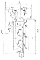
- FIG. 1 is a block diagram illustrating a multistage transconductor and filter circuit 15 according to an exemplary embodiment of the invention.
- the multistage transconductor and filter circuit 100 includes multiple similar stages 101.
- each stage 101 is a transconductor and filter circuit, which includes a front end module 102 coupled to a filter module 103, as described in further detail below.
- the front end module 102 and the filter module 103 may be implemented on separate circuits.
- the front end module 102 receives a differential input voltage signal (V IN ) 111 and converts the differential input voltage signal 111 into a differential output current (I OUT ) 112.
- the filter module 103 receives the differential output current 112 and outputs a differential output voltage signal (V OUT ) 113, which is further supplied to a subsequent stage 101 within the multistage transconductor and filter circuit 100.
- FIG. 2 is a circuit, diagram illustrating an exemplary prior art front end module within one stage of the multistage transconductor and filter circuit.
- the front end module 102 is a differential amplifier, such as, for example, a triple differential amplifier or "triplet" circuit, as described in further detail in " The Multi-tanh Principle: A tutorial Overview," by Barrie Gilbert, published in the IEEE Journal of Solid-State Circuits, Vol. 33, No. 1, January 1998 .
- the front end module 102 includes one or more differential transistor pairs configured to convert V IN 111 into I OUT 112.
- the front end module 102 shown in Figure 2 includes three differential pairs of transistors 201-202, 203-204, and 205-206, having inputs and outputs coupled in parallel.
- the emitters of each differential transistor pair 201 -202, 203-204, 205-206 are coupled to corresponding collectors of transistors 207, 208, 209.
- the bases of transistors 207, 208, 209 are coupled to receive a bias voltage V BIAS .
- the outer differential pairs 201-202 and 205-206 have opposing emitter-area ratios of A and operate at equal tail currents.
- the emitter bias current transmitted to this center pair 203-204 is set to K times the emitter bias current transmitted to the outer pairs, where K is a factor less than 1.
- K is a factor less than 1.
- Figure 3 is a graph illustrating the effective transconductance g M as a function of the differential input voltage V IN 111 for the prior art front end module 102.
- the graphic representations 301, 302, and 303 correspond to the differential transistor pairs 201-202, 203-204, and 205-206, respectively, and are offset due to the performance of each respective differential transistor pair.
- a composite graphic representation 304 illustrates the transconductance g M of the front end module 102 as a function of the differential input voltage V IN 111.
- FIG. 4 is a circuit diagram illustrating a transconductor and filter circuit 101 according to an exemplary embodiment of the invention.
- the transconductor and filter circuit 101 includes a front end module 102 similar to the front end module described in detail in connection with Figure 2, having three differential pairs of transistor devices 401-402, 403-404, and 405-406, having inputs and outputs coupled in parallel.
- the circuit 101 may include any number of differential transistor pairs.
- the emitters of each differential transistor pair 401-402, 403-404, 405-406 are coupled to corresponding collectors of transistor devices 401, 408, 409.
- the bases of transistor devices 407, 408, 409 are coupled to receive a bias voltage V BIAS .
- the differential output current 112 is supplied to the filter module 103 at the output of the front end module 102.
- the filter module 103 includes resistor devices (R 1 ) 411, 412, 413 and 414. Each resistor device 411, 412 is coupled from V CC to each output current 112. This arrangement converts the differential output current 112 into an intermediary differential voltage.
- Each resistor device 413, 414 is coupled in series to one line of the differential output of the front end module 102.
- the resistor devices 411, 412, 413 and 414 have an identical resistance value R 1 .
- the filter module 103 further includes capacitor devices 415 and 416 coupled to the corresponding resistor devices 413 and 414.
- a further capacitor device 417 is coupled between the two resistor devices 413 and 414.
- the capacitor devices 415 and 416 have an identical capacitance value C 1 and the capacitor device 417 has a capacitance value C 2 .
- the resistor devices 413, 414 and the capacitor devices 415, 416, and 417 may be implemented on a separate circuit coupled to the front end module 102.
- the differential voltage is further supplied to a pair of emitter followers 418, 419.
- the voltage gain of the emitter followers 418, 419 has a value of less than 1 and provides a low output impedance to drive a subsequent stage 101.
- the base of each transistor device 418, 419 is coupled to a respective resistor device 413, 414.
- the emitter of each transistor device 418, 419 is coupled to a corresponding collector of transistor devices 421, 422, which have their bases coupled to receive a bias voltage V11
- g M is the effective transconductance of the circuit 101
- ⁇ 0 is the corner frequency of the filter module 103
- a is a coefficient determined by the selection of the resistance R 1 , and of the capacitances C 1
- C 2 and g M R 1 is the effective gain of the circuit 101.
- the low pass filter function can thus be implemented with a voltage gain of g M R 1 .
- FIG. 5 is a graph illustrating the total transconductance for the transconductor and filter circuit 101 according to an exemplary embodiment of the invention
- the total transconductance g M . as a function of the differential input voltage V IN 111 is a composite of the transconductance values for the corresponding differential transistor pairs 401-402, 403-404, 405-406, which are displaced in center voltage.
- the circuit 101 has a broader signal handling range before it becomes non-linear.
- Figure 6 is a graph illustrating the effective gain for the transconductor and fitter circuit 101 according to an exemplary embodiment of the invention.
- the effective gain of the circuit 101 which is defined as the differential voltage across the two resistors 411 and 412 divided by the differential input voltage 111, is a function of the transconductance g M times the value R 1 of the resistors 411, 412.
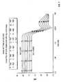
- Figure us a graph illustrating the voltage gain of a fourth order Butterworth filter for various values of a control current I AGC according to an exemplary embodiment of the invention.
- the voltage gain in decibels (dB)
- dB decibels
- ⁇ A microAmpers
- a fourth order Butterworth filter is implemented with two transconductor and filter circuits 101 cascaded together, as shown in the multistage circuit 100 of Figure 1.
- the two transconductor and filter circuits 101 are not identical, having different values for the capacitance of capacitors 415, 416 and 417.
- a Bessel filter may be implemented using the transconductor and filter circuit 101.
- an approximation of a Gaussian filter may be implemented using the transconductor and filter circuit 101.
- a transitional filter may be implemented using the transconductor and filter circuit 101.
- R 1 C 1 ' and C 2 ' are the values used in Figure x with two cascaded sections. These values directly map into the differential circuit of Figure 4 with the exception of C 2 ' which maps into Figure 4 with a scale factor of 1 ⁇ 2 % due to the differential nature of Figure 4.
- FIG. 8 is a flow diagram illustrating a method for low pass filtering within the transconductor and filter circuit according to an exemplary embodiment of the invention.
- a differential input voltage signal is received at processing block 801 at processing block 802.
- the differential input voltage signal is converted into a differential output current.
- the differential output current is converted into an intermediary differential voltage.
- the intermediary differential voltage is filtered to obtain a filtered differential output voltage signal having low output impedance.
- embodiments of the present invention may be implemented not only within a physical circuit (e.g. on a semiconductor chip), but also within machine-readable media.
- the circuits and designs discussed above may be stored upon and/or embedded within machine-readable media associated with a design tool used for designing semiconductor devices. Examples include a netlist formatted in the VHSIC Hardware Description Language (VHDL). Verilog language, or Spice language.
- VHDL VHSIC Hardware Description Language
- Verilog language Verilog language
- Spice language Spice
- Some netlist examples include: a behavioral level netlist, a register transfer level (RTL) netlist, a gate level netlist, and a transistor level netlist.
- Machine-readable media also include media having layout information such as a GUS-II file.
- netlist files or other machine-readable media for semiconductor chip design may be used in a simulation environment to perform the methods of the teachings described above.
- embodiments of this invention may be used as or to support a software program executed upon some form of a processing core (such as the CPU of a computer) or otherwise implemented or realized upon or within a machine-readable medium, which includes any mechanism for storing or transmitting information in a form readable by a machine (e.g. a computer).
Applications Claiming Priority (1)
| Application Number | Priority Date | Filing Date | Title |
|---|---|---|---|
| US11/510,443 US7504879B2 (en) | 2006-08-24 | 2006-08-24 | Transconductor and filter circuit |
Publications (2)
| Publication Number | Publication Date |
|---|---|
| EP1892833A2 true EP1892833A2 (de) | 2008-02-27 |
| EP1892833A3 EP1892833A3 (de) | 2011-07-13 |
Family
ID=38662630
Family Applications (1)
| Application Number | Title | Priority Date | Filing Date |
|---|---|---|---|
| EP20070114767 Ceased EP1892833A3 (de) | 2006-08-24 | 2007-08-22 | Transkonduktor und Filterschaltung |
Country Status (3)
| Country | Link |
|---|---|
| US (1) | US7504879B2 (de) |
| EP (1) | EP1892833A3 (de) |
| AU (1) | AU2007211908B2 (de) |
Families Citing this family (1)
| Publication number | Priority date | Publication date | Assignee | Title |
|---|---|---|---|---|
| RU2507676C1 (ru) * | 2012-08-14 | 2014-02-20 | Федеральное государственное бюджетное образовательное учреждение высшего профессионального образования "Южно-Российский государственный университет экономики и сервиса" (ФГБОУ ВПО "ЮРГУЭС") | Избирательный усилитель |
Citations (3)
| Publication number | Priority date | Publication date | Assignee | Title |
|---|---|---|---|---|
| US5293087A (en) * | 1991-10-17 | 1994-03-08 | Fujitsu Limited | Filter circuit and filter integrated circuit |
| US6381449B1 (en) * | 1998-06-30 | 2002-04-30 | Kabushiki Kaisha Toshiba | Frequency converter |
| EP1689082A1 (de) * | 2005-02-02 | 2006-08-09 | Stmicroelectronics SA | Ein rauscharmes Tiefpassfilter |
Family Cites Families (47)
| Publication number | Priority date | Publication date | Assignee | Title |
|---|---|---|---|---|
| US3829774A (en) | 1970-09-08 | 1974-08-13 | Triplett Corp | Micropower autopolarity voltmeter |
| US3746984A (en) | 1970-09-08 | 1973-07-17 | Triplett Corp | Autopolarity voltmeter circuit |
| FR2561468B1 (fr) | 1984-03-13 | 1989-10-20 | Thomson Csf | Filtre actif hyperfrequence |
| GB2168864A (en) | 1984-12-19 | 1986-06-25 | Philips Electronic Associated | Radio receiver/transmitter filters |
| GB2191660B (en) | 1986-06-14 | 1990-04-25 | Marconi Instruments Ltd | Measuring adjacent channel power |
| FR2694149B1 (fr) | 1992-07-21 | 1994-09-30 | Ezran Philippe | Procédé et dispositif de démodulation tout numérique de signal analogique. |
| JPH06244889A (ja) | 1993-02-15 | 1994-09-02 | Fujitsu Ltd | モデム復調部用受信レベル調整回路 |
| US5495200A (en) | 1993-04-06 | 1996-02-27 | Analog Devices, Inc. | Double sampled biquad switched capacitor filter |
| US5381148A (en) | 1993-07-12 | 1995-01-10 | Analog Devices, Inc. | Method and apparatus for calibrating a gain control circuit |
| JPH07245546A (ja) * | 1994-03-03 | 1995-09-19 | Nippon Motorola Ltd | アクティブローパスフィルタ |
| US6011431A (en) | 1994-11-23 | 2000-01-04 | Analog Devices, Inc. | Automatically tracking multiple-pole active filter |
| US5606731A (en) | 1995-03-07 | 1997-02-25 | Motorola, Inc. | Zerox-IF receiver with tracking second local oscillator and demodulator phase locked loop oscillator |
| US6111911A (en) | 1995-06-07 | 2000-08-29 | Sanconix, Inc | Direct sequence frequency ambiguity resolving receiver |
| US5623744A (en) | 1995-12-08 | 1997-04-29 | Triplett; Timothy | Vacuum cleaner |
| US5901347A (en) | 1996-01-17 | 1999-05-04 | Motorola, Inc. | Fast automatic gain control circuit and method for zero intermediate frequency receivers and radiotelephone using same |
| KR100188692B1 (ko) | 1996-01-20 | 1999-06-01 | 윤종용 | 디지탈필터 |
| US5949820A (en) | 1996-08-01 | 1999-09-07 | Nec Electronics Inc. | Method for optimizing an equalization and receive filter |
| US6138190A (en) | 1997-09-16 | 2000-10-24 | Cirrus Logic, Inc. | Analog front end and digital signal processing device and method |
| US6014554A (en) | 1997-09-30 | 2000-01-11 | Lucent Technologies, Inc. | Method and apparatus for tuning analog filters |
| FR2774831B1 (fr) | 1998-02-11 | 2000-04-07 | Agence Spatiale Europeenne | Recepteur adaptatif de signaux pour systeme de communications a acces pultiples par repartition a codes |
| US6064277A (en) | 1998-02-27 | 2000-05-16 | Analog Devices, Inc. | Automatic biasing scheme for reducing oscillator phase noise |
| WO2000044090A1 (fr) | 1999-01-19 | 2000-07-27 | Hitachi, Ltd. | Circuit integre a semiconducteur |
| US6317016B1 (en) | 1999-05-14 | 2001-11-13 | Koninklijke Philips Electronics | Method and arrangement for gyration filtering with low power consumption |
| US6407658B2 (en) | 1999-05-14 | 2002-06-18 | Koninklijke Philips Electronics N.V. | Method and arrangement for filtering with common mode feedback for low power consumption |
| US6262623B1 (en) | 1999-05-28 | 2001-07-17 | Conexant Systems, Inc. | Log-domain filter having a variable dynamic range window |
| KR100450932B1 (ko) | 1999-06-24 | 2004-10-02 | 삼성전자주식회사 | 이중모드 단말기에서 가변대역 기저대역 필터링을 위한 아날로그 복조장치 |
| US6194958B1 (en) | 1999-09-30 | 2001-02-27 | Analog Devices, Inc. | Filter having minimized cut-off frequency variations |
| US6335656B1 (en) | 1999-09-30 | 2002-01-01 | Analog Devices, Inc. | Direct conversion receivers and filters adapted for use therein |
| JP2001119268A (ja) | 1999-10-21 | 2001-04-27 | Matsushita Electric Ind Co Ltd | フィルタ調整方法及びフィルタ調整装置 |
| DE19962760A1 (de) * | 1999-12-23 | 2001-06-28 | Rohde & Schwarz | Anordnung zum Erzeugen eines analogen I/Q-Signals aus zwei oder mehreren Datenströmen |
| US6429720B1 (en) | 2000-05-12 | 2002-08-06 | Analog Devices, Inc. | RMS-DC converter using a variable gain amplifier to drive a squaring cell |
| DE10004996C2 (de) | 2000-02-04 | 2002-09-26 | Infineon Technologies Ag | Vorrichtung und Verfahren zur Selbstkalibrierung von Faltungs-Analog/Digitalwandlern |
| GB2359680B (en) | 2000-02-25 | 2002-05-15 | Motorola Israel Ltd | Apparatus for linear transmitter with improved loop gain stabilization |
| EP1128547A3 (de) | 2000-02-28 | 2001-09-05 | Deutsche Thomson-Brandt Gmbh | Gilbert-Multiplizierer-Zelle Mischer |
| JP3489621B2 (ja) | 2000-09-28 | 2004-01-26 | 日本電気株式会社 | ダイレクトコンバージョン受信機のベースバンド回路 |
| US6433626B1 (en) | 2001-01-16 | 2002-08-13 | Motorola, Inc. | Current-mode filter with complex zeros |
| EP1233319A1 (de) | 2001-02-15 | 2002-08-21 | STMicroelectronics Limited | Stromquelle |
| JP3584893B2 (ja) | 2001-03-14 | 2004-11-04 | ソニー株式会社 | フィルタ回路 |
| EP1289123A1 (de) | 2001-08-10 | 2003-03-05 | Asulab S.A. | Frequenzumsetzer für ein GPS-Empfänger |
| US6683505B2 (en) * | 2001-08-24 | 2004-01-27 | Koninklijke Philips Electronics N.V. | High speed voltage controlled oscillator |
| US20030080811A1 (en) | 2001-10-05 | 2003-05-01 | Toshifumi Nakatani | Variable gain amplifying apparatus and wireless communication apparatus |
| US6602438B2 (en) | 2001-12-07 | 2003-08-05 | Protectronics Technology Corporation | Structure for polymeric thermistor and method of making the same |
| JP2003298441A (ja) | 2002-04-01 | 2003-10-17 | Hitachi Ltd | 低消費電力受信装置 |
| US6661267B2 (en) * | 2002-05-06 | 2003-12-09 | International Business Machines Corporation | Coarse calibration circuit using variable step sizes to reduce jitter and a dynamic course calibration (DCC) circuit for a 2 GHz VCO |
| US6686801B1 (en) | 2002-07-23 | 2004-02-03 | Mediatek Inc. | Power amplifier with distributed capacitor |
| US7002403B2 (en) * | 2002-09-13 | 2006-02-21 | Broadcom Corporation | Transconductance/C complex band-pass filter |
| US7215182B2 (en) * | 2005-09-12 | 2007-05-08 | Analog Devices, Inc. | High-performance, low-noise reference generators |
-
2006
- 2006-08-24 US US11/510,443 patent/US7504879B2/en active Active
-
2007
- 2007-08-22 EP EP20070114767 patent/EP1892833A3/de not_active Ceased
- 2007-08-23 AU AU2007211908A patent/AU2007211908B2/en active Active
Patent Citations (3)
| Publication number | Priority date | Publication date | Assignee | Title |
|---|---|---|---|---|
| US5293087A (en) * | 1991-10-17 | 1994-03-08 | Fujitsu Limited | Filter circuit and filter integrated circuit |
| US6381449B1 (en) * | 1998-06-30 | 2002-04-30 | Kabushiki Kaisha Toshiba | Frequency converter |
| EP1689082A1 (de) * | 2005-02-02 | 2006-08-09 | Stmicroelectronics SA | Ein rauscharmes Tiefpassfilter |
Non-Patent Citations (4)
| Title |
|---|
| PENG-UN SU ET AL: "A 0.25/spl mu/m CMOS OPLL transmitter IC for GSM and DCS", RADIO FREQUENCY INTEGRATED CIRCUITS (RFIC) SYMPOSIUM, 2004. DIGEST OF PAPERS. 2004 IEEE FORT WORTH, TX, USA JUNE 6-8, 2004, PISCATAWAY, NJ, USA,IEEE, 6 June 2004 (2004-06-06), pages 435 - 438, XP010713849, ISBN: 978-0-7803-8333-3, DOI: 10.1109/RFIC.2004.1320645 * |
| WYATT M A: "ACTIVE FILTER GETS HIGHER FREQUENCIES", ELECTRONIC DESIGN, PENTON MEDIA, CLEVELAND, OH, US, vol. 39, no. 16, 22 August 1991 (1991-08-22), pages 108, XP000259742, ISSN: 0013-4872 * |
| WYATT M A: "FILTER IMPROVES STOP-BAND REJECTION", ELECTRONIC DESIGN, PENTON MEDIA, CLEVELAND, OH, US, vol. 42, no. 11, 30 May 1994 (1994-05-30), pages 92, XP000464762, ISSN: 0013-4872 * |
| WYATT M: "ACTIVE FILTER MAKES COMPONENT SELECTION EASIER", EDN ELECTRICAL DESIGN NEWS, REED BUSINESS INFORMATION, HIGHLANDS RANCH, CO, US, vol. 37, no. 2, 20 January 1992 (1992-01-20), pages 136, XP000281184, ISSN: 0012-7515 * |
Also Published As
| Publication number | Publication date |
|---|---|
| AU2007211908B2 (en) | 2011-03-24 |
| AU2007211908A1 (en) | 2008-03-13 |
| EP1892833A3 (de) | 2011-07-13 |
| US7504879B2 (en) | 2009-03-17 |
| US20080122530A1 (en) | 2008-05-29 |
Similar Documents
| Publication | Publication Date | Title |
|---|---|---|
| Gilmore et al. | Practical RF Circuit Design for Modern Wireless Systems: Active Circuits and Systems, Volume 2 | |
| KR970008793B1 (ko) | 필터 장치 | |
| Yuce et al. | CCII-based PID controllers employing grounded passive components | |
| US20060164159A1 (en) | Filter circuit | |
| EP1977507A1 (de) | Verstärker mit mehreren eingängen und mehreren ausgängen | |
| Ferri et al. | High-valued passive element simulation using low-voltage low-power current conveyors for fully integrated applications | |
| US4147997A (en) | Active filters utilizing networks of resistors and negative impedance converters | |
| EP1892833A2 (de) | Transkonduktor und Filterschaltung | |
| EP1993202A1 (de) | Ausgeglichener Operationsverstärker und aktiver RC-Filter mit einem derartigen Verstärker | |
| JP2571811B2 (ja) | 集積能動電子フィルタ | |
| SE508697C2 (sv) | Förfarande och anordning för tidskontinuerlig filtrering i digital CMOS-process | |
| US20200220509A1 (en) | Trans-Impedance Amplifier, Chip, and Communications Device | |
| US7522023B2 (en) | Gyrator with feedback resistors | |
| US6239653B1 (en) | Biquadratic basic cell for programmable analog time-continuous filter | |
| JP2539301B2 (ja) | 有極型リ−プフロッグ・フィルタ | |
| JP3005413B2 (ja) | フィルタ回路 | |
| EP1424773A1 (de) | Schaltungsvorrichtung zur Herstellung eines nicht-lineares Skaliernetzwerk mit reaktiven Elementen | |
| JP2809994B2 (ja) | 完全に差動的な非演算増幅器に基づく正帰還形のバイポーラ接合形トランジスタバイクワッドフィルタ | |
| JP2000236266A (ja) | アナログ復号化装置 | |
| Malcher et al. | Digitally programmable modified current differencing transconductance amplifier in 40‐nm technology: design flow, parameter analyses and applications | |
| JPH01316014A (ja) | アクティブフィルター回路 | |
| CN116842886A (zh) | 一种通用的传递函数电路建模的模块化方法 | |
| US7138869B2 (en) | Amplifier circuit | |
| JPH10198909A (ja) | 磁気情報読取り装置 | |
| El Feki et al. | Optimization of a rail to rail low voltage current conveyor and high frequency current-mode filter applications |
Legal Events
| Date | Code | Title | Description |
|---|---|---|---|
| PUAI | Public reference made under article 153(3) epc to a published international application that has entered the european phase |
Free format text: ORIGINAL CODE: 0009012 |
|
| AK | Designated contracting states |
Kind code of ref document: A2 Designated state(s): AT BE BG CH CY CZ DE DK EE ES FI FR GB GR HU IE IS IT LI LT LU LV MC MT NL PL PT RO SE SI SK TR |
|
| AX | Request for extension of the european patent |
Extension state: AL BA HR MK YU |
|
| PUAL | Search report despatched |
Free format text: ORIGINAL CODE: 0009013 |
|
| AK | Designated contracting states |
Kind code of ref document: A3 Designated state(s): AT BE BG CH CY CZ DE DK EE ES FI FR GB GR HU IE IS IT LI LT LU LV MC MT NL PL PT RO SE SI SK TR |
|
| AX | Request for extension of the european patent |
Extension state: AL BA HR MK RS |
|
| 17P | Request for examination filed |
Effective date: 20110801 |
|
| 17Q | First examination report despatched |
Effective date: 20111017 |
|
| AKX | Designation fees paid |
Designated state(s): DE FR GB |
|
| RAP1 | Party data changed (applicant data changed or rights of an application transferred) |
Owner name: EXELIS INC. |
|
| STAA | Information on the status of an ep patent application or granted ep patent |
Free format text: STATUS: THE APPLICATION HAS BEEN REFUSED |
|
| 18R | Application refused |
Effective date: 20150420 |