EP1887635B1 - Light-emitting device - Google Patents
Light-emitting device Download PDFInfo
- Publication number
- EP1887635B1 EP1887635B1 EP07015539.5A EP07015539A EP1887635B1 EP 1887635 B1 EP1887635 B1 EP 1887635B1 EP 07015539 A EP07015539 A EP 07015539A EP 1887635 B1 EP1887635 B1 EP 1887635B1
- Authority
- EP
- European Patent Office
- Prior art keywords
- light
- substrate
- emitting element
- emitting device
- external connection
- Prior art date
- Legal status (The legal status is an assumption and is not a legal conclusion. Google has not performed a legal analysis and makes no representation as to the accuracy of the status listed.)
- Active
Links
Images

Classifications
-
- H—ELECTRICITY
- H10—SEMICONDUCTOR DEVICES; ELECTRIC SOLID-STATE DEVICES NOT OTHERWISE PROVIDED FOR
- H10H—INORGANIC LIGHT-EMITTING SEMICONDUCTOR DEVICES HAVING POTENTIAL BARRIERS
- H10H20/00—Individual inorganic light-emitting semiconductor devices having potential barriers, e.g. light-emitting diodes [LED]
- H10H20/80—Constructional details
- H10H20/85—Packages
- H10H20/857—Interconnections, e.g. lead-frames, bond wires or solder balls
-
- H—ELECTRICITY
- H01—ELECTRIC ELEMENTS
- H01L—SEMICONDUCTOR DEVICES NOT COVERED BY CLASS H10
- H01L2224/00—Indexing scheme for arrangements for connecting or disconnecting semiconductor or solid-state bodies and methods related thereto as covered by H01L24/00
- H01L2224/01—Means for bonding being attached to, or being formed on, the surface to be connected, e.g. chip-to-package, die-attach, "first-level" interconnects; Manufacturing methods related thereto
- H01L2224/02—Bonding areas; Manufacturing methods related thereto
- H01L2224/04—Structure, shape, material or disposition of the bonding areas prior to the connecting process
- H01L2224/05—Structure, shape, material or disposition of the bonding areas prior to the connecting process of an individual bonding area
- H01L2224/0554—External layer
- H01L2224/0556—Disposition
- H01L2224/0557—Disposition the external layer being disposed on a via connection of the semiconductor or solid-state body
-
- H—ELECTRICITY
- H01—ELECTRIC ELEMENTS
- H01L—SEMICONDUCTOR DEVICES NOT COVERED BY CLASS H10
- H01L2224/00—Indexing scheme for arrangements for connecting or disconnecting semiconductor or solid-state bodies and methods related thereto as covered by H01L24/00
- H01L2224/01—Means for bonding being attached to, or being formed on, the surface to be connected, e.g. chip-to-package, die-attach, "first-level" interconnects; Manufacturing methods related thereto
- H01L2224/02—Bonding areas; Manufacturing methods related thereto
- H01L2224/04—Structure, shape, material or disposition of the bonding areas prior to the connecting process
- H01L2224/05—Structure, shape, material or disposition of the bonding areas prior to the connecting process of an individual bonding area
- H01L2224/0554—External layer
- H01L2224/0556—Disposition
- H01L2224/05571—Disposition the external layer being disposed in a recess of the surface
-
- H—ELECTRICITY
- H01—ELECTRIC ELEMENTS
- H01L—SEMICONDUCTOR DEVICES NOT COVERED BY CLASS H10
- H01L2224/00—Indexing scheme for arrangements for connecting or disconnecting semiconductor or solid-state bodies and methods related thereto as covered by H01L24/00
- H01L2224/01—Means for bonding being attached to, or being formed on, the surface to be connected, e.g. chip-to-package, die-attach, "first-level" interconnects; Manufacturing methods related thereto
- H01L2224/02—Bonding areas; Manufacturing methods related thereto
- H01L2224/04—Structure, shape, material or disposition of the bonding areas prior to the connecting process
- H01L2224/05—Structure, shape, material or disposition of the bonding areas prior to the connecting process of an individual bonding area
- H01L2224/0554—External layer
- H01L2224/05573—Single external layer
-
- H—ELECTRICITY
- H01—ELECTRIC ELEMENTS
- H01L—SEMICONDUCTOR DEVICES NOT COVERED BY CLASS H10
- H01L2224/00—Indexing scheme for arrangements for connecting or disconnecting semiconductor or solid-state bodies and methods related thereto as covered by H01L24/00
- H01L2224/01—Means for bonding being attached to, or being formed on, the surface to be connected, e.g. chip-to-package, die-attach, "first-level" interconnects; Manufacturing methods related thereto
- H01L2224/10—Bump connectors; Manufacturing methods related thereto
- H01L2224/15—Structure, shape, material or disposition of the bump connectors after the connecting process
- H01L2224/16—Structure, shape, material or disposition of the bump connectors after the connecting process of an individual bump connector
- H01L2224/161—Disposition
- H01L2224/16151—Disposition the bump connector connecting between a semiconductor or solid-state body and an item not being a semiconductor or solid-state body, e.g. chip-to-substrate, chip-to-passive
- H01L2224/16221—Disposition the bump connector connecting between a semiconductor or solid-state body and an item not being a semiconductor or solid-state body, e.g. chip-to-substrate, chip-to-passive the body and the item being stacked
- H01L2224/16225—Disposition the bump connector connecting between a semiconductor or solid-state body and an item not being a semiconductor or solid-state body, e.g. chip-to-substrate, chip-to-passive the body and the item being stacked the item being non-metallic, e.g. insulating substrate with or without metallisation
-
- H—ELECTRICITY
- H01—ELECTRIC ELEMENTS
- H01L—SEMICONDUCTOR DEVICES NOT COVERED BY CLASS H10
- H01L2224/00—Indexing scheme for arrangements for connecting or disconnecting semiconductor or solid-state bodies and methods related thereto as covered by H01L24/00
- H01L2224/01—Means for bonding being attached to, or being formed on, the surface to be connected, e.g. chip-to-package, die-attach, "first-level" interconnects; Manufacturing methods related thereto
- H01L2224/42—Wire connectors; Manufacturing methods related thereto
- H01L2224/47—Structure, shape, material or disposition of the wire connectors after the connecting process
- H01L2224/48—Structure, shape, material or disposition of the wire connectors after the connecting process of an individual wire connector
- H01L2224/4805—Shape
- H01L2224/4809—Loop shape
- H01L2224/48091—Arched
-
- H—ELECTRICITY
- H01—ELECTRIC ELEMENTS
- H01L—SEMICONDUCTOR DEVICES NOT COVERED BY CLASS H10
- H01L2224/00—Indexing scheme for arrangements for connecting or disconnecting semiconductor or solid-state bodies and methods related thereto as covered by H01L24/00
- H01L2224/73—Means for bonding being of different types provided for in two or more of groups H01L2224/10, H01L2224/18, H01L2224/26, H01L2224/34, H01L2224/42, H01L2224/50, H01L2224/63, H01L2224/71
- H01L2224/732—Location after the connecting process
- H01L2224/73251—Location after the connecting process on different surfaces
- H01L2224/73265—Layer and wire connectors
-
- H—ELECTRICITY
- H01—ELECTRIC ELEMENTS
- H01L—SEMICONDUCTOR DEVICES NOT COVERED BY CLASS H10
- H01L2924/00—Indexing scheme for arrangements or methods for connecting or disconnecting semiconductor or solid-state bodies as covered by H01L24/00
- H01L2924/0001—Technical content checked by a classifier
- H01L2924/00014—Technical content checked by a classifier the subject-matter covered by the group, the symbol of which is combined with the symbol of this group, being disclosed without further technical details
-
- H—ELECTRICITY
- H01—ELECTRIC ELEMENTS
- H01L—SEMICONDUCTOR DEVICES NOT COVERED BY CLASS H10
- H01L2924/00—Indexing scheme for arrangements or methods for connecting or disconnecting semiconductor or solid-state bodies as covered by H01L24/00
- H01L2924/01—Chemical elements
- H01L2924/01078—Platinum [Pt]
-
- H—ELECTRICITY
- H01—ELECTRIC ELEMENTS
- H01L—SEMICONDUCTOR DEVICES NOT COVERED BY CLASS H10
- H01L2924/00—Indexing scheme for arrangements or methods for connecting or disconnecting semiconductor or solid-state bodies as covered by H01L24/00
- H01L2924/01—Chemical elements
- H01L2924/01079—Gold [Au]
-
- H—ELECTRICITY
- H10—SEMICONDUCTOR DEVICES; ELECTRIC SOLID-STATE DEVICES NOT OTHERWISE PROVIDED FOR
- H10H—INORGANIC LIGHT-EMITTING SEMICONDUCTOR DEVICES HAVING POTENTIAL BARRIERS
- H10H20/00—Individual inorganic light-emitting semiconductor devices having potential barriers, e.g. light-emitting diodes [LED]
- H10H20/80—Constructional details
- H10H20/85—Packages
- H10H20/8506—Containers
Definitions
- the present invention relates to a light-emitting device, and more particularly, to a light-emitting device which can effectively use light from a light-emitting element connected to a wiring substrate.
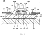
- Fig. 1 is a sectional view illustrating a known light-emitting device.
- a light-emitting device 100 includes a light-emitting element 101, a sub-mount substrate 102, a board substrate 103, external connection terminals 104 and 105, and a heat-sinking plate 107.
- the light-emitting element 101 is an element which emits light from the entire surface thereof.
- the light-emitting element 101 has power supply terminals 111 and 112.
- the light-emitting element 101 is connected to the sub-mount substrate 102 in a flip-chip bonding manner.
- the sub-mount substrate is fixed to the board substrate 103 by the use of a bonding method using an Au-Sn alloy which has thermal conductivity higher than solder.
- the sub-mount substrate 102 includes a substrate body 114 and wiring patterns 115 and 116.
- the substrate body 114 serves to mount the wiring patterns 115 and 116 thereon.
- the substrate body 114 can be made of a material having high thermal conductivity, such as AlN.
- the wiring patterns 115 and 116 are formed on the substrate body 114.
- the wiring pattern 115 is electrically connected to the power supply terminal 111 via a bump 118 and the wiring pattern 116 is electrically connected to the power supply terminal 112 via a bump 118.
- the sub-mount substrate 102 serves to raise the light-emitting element 101 so as to protrude higher than the top surfaces 104A and 105A of portions of the external connection leads 104 and 105, in which the portions are disposed on the board substrate 103.
- the board substrate 103 includes a substrate body 121 and wiring patterns 122 and 123.
- the substrate body 121 serves to mount the wiring patterns 122 and 123 thereon.
- the substrate body 121 can be made of a material having high thermal conductivity, such as AlN or ceramic.
- the wiring patterns 122 and 123 are disposed on the substrate body 121.
- the wiring pattern 122 is electrically connected to the wiring pattern 115 via a wire 125A.
- the wiring pattern 123 is electrically connected to the wiring pattern 116 via a wire 125B. That is, the sub-mount substrate 102 is connected to the board substrate 103 in a wire bonding manner.
- the external connection terminal 104 is fixed onto the wiring pattern 122 using Ag paste 127 as an adhesive.
- the external connection lead 105 is fixed onto the wiring pattern 123 using the Ag paste 127 as an adhesive.
- the heat-sinking plate 107 is fixed onto the bottom surface of the substrate body 121 by using Ag paste.
- the heat-sinking plate 107 serves to release heat, which is generated when the light-emitting element 101 emits light, outside the light-emitting device 100.
- the heat which is generated when the light-emitting element 101 emits light is transmitted to the heat-sinking plate 107 via the sub-mount substrate 102 and the board substrate 103 (see Unexamined Japanese Patent Application Publication No. 2005-203448 ).
- the related-art light-emitting device 100 has a problem with increase in cost because the sub-mount substrate 102 is fixed to the board substrate 103 using an expensive material of an Au-Sn alloy by the use of an Au-Sn bonding method.
- JP 2005-109282 describes a face-down type LED element which is mounted on a sub-mount loaded on a metallic base part. Thereby, heat of the LED element which may be generated at the time of power supply is transmitted to the metallic base part through the sub-mount and discharged by the metallic base part. Tip parts of lead parts are attached to and connected to both sides of the sub-mount in a state insulated from the metallic base part
- EP 1 231 650 describes a reflector-containing semiconductor component which comprises a radiation-emitting LED. The semiconductor component is seated in a housing which comprises at least one base part and a reflector for the radiation from the LED, the LED being fastened on a platform in the vertex of the reflector.
- JP S5-124886 describes another LED element.
- JP 2006-135276 describes a semiconductor light emitting element mounting package.
- the mounting package comprises a silicon substrate having a region in which a semiconductor light emitting element is mounted.
- a groove surrounding the mounting region for the semiconductor light emitting element is formed on the surface, and a reflecting film is formed on the inner surface of the groove.
- the sub-mount substrate provided in the related-art light-emitting device becomes unnecessary because the light-emitting device uses the substrate body having the protruding portion at the position where the light-emitting element is disposed. It is therefore possible to effectively use light emitted from the entire surface of the light-emitting element while reducing the cost thereof.
- the Au-Sn bonding method which incurs high cost becomes unnecessary, the cost of the light-emitting device can be reduced.
- the substrate body having the protruding portion at the position where the light-emitting element is disposed is provided, the wiring pattern electrically connected to the first power supply terminal is formed on the surface of the substrate body on which the protruding portion is disposed, the penetrating electrode which penetrates the substrate body is formed in the protruding portion, and the penetrating electrode is electrically connected to the second power supply terminal. Accordingly, it is possible to effectively use light emitted from the entire surface of the light-emitting element and it is possible to reduce the size of the substrate body, resulting in cost reduction of the light-emitting device.
- light emitted from the entire surface of the light-emitting element can be effectively used and the cost of the light-emitting device can be reduced.
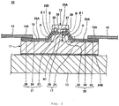
- Fig. 2 is a cross-sectional view illustrating a light-emitting device according to a first embodiment of the invention.
- the light-emitting device 100 includes a wiring substrate 11, a light-emitting element 12, a heat-sinking plate 13 and external connection leads 14 and 15.
- the wiring substrate 11 includes a substrate body 17, an insulation layer 18, a first wiring pattern 21 and a second wiring pattern 22.
- the substrate body 17 comprises a substrate portion 21 and a protruding portion 25.
- the protruding portion 25 is integrated into the substrate portion 24.
- the protruding portion 25 is formed on the top surface 24A of the substrate portion 24 and protrudes from the top surface 24A of the substrate portion 24.
- the top surface 25A of the protruding portion 25 protrudes higher than the top surface 14A of the external connection lead 14 disposed on the first wiring pattern 21 and the top surface 15A of external connection lead 15 disposed on the second wiring pattern 22.
- the protruding portion 25 serves to enable the light-emitting element 12 to be positioned higher than the top surface 14A of the external connection lead 14 and the top surface 15A of the external connection lead 15 at positions where the external connection leads 14 and 15 are disposed on the first wiring pattern 21 and the second wiring pattern 22, respectively.
- a height H1 (height measured when the top surface 24A of the substrate portion 24 is a base level) of the protruding portion 25 can be about 400 ⁇ m.
- the sub-mount substrate 102 provided in the related-art light-emitting device 100 becomes unnecessary.
- the light-emitting device 10 use two substrates (the sub-mount substrate 102 and the board substrate 103) like the related-art light-emitting device 100. That is, a single substrate (the wiring substrate 11) is enough to use for the light-emitting device 10. Accordingly, the cost of the light-emitting device 10 can be reduced.
- the protruding portion 25 takes a form of which a width decreases toward an upper portion (the top surface 25A of the protruding portion 25) from a lower portion thereof.
- a side surface 25B of the protruding portion 25 is an inclined surface inclined at an angle of ⁇ 1 with respect to the top surface 24A of the substrate portion 24.
- the angle ⁇ 1 can be, for example, 54.7° or 90°.
- a material for the substrate body 17 can be silicon.
- An advantage of using silicon as a material for the substrate body 17 is that it is easy to form the protruding portion 25 having the inclined side surface 25B.
- the insulation layer is formed on the top surface 24A of the substrate portion 24 and the top surface 25A and the side surface 25B of the protruding portion 25.
- the insulation layer 18 serves to insulate the first and second wiring patterns 21 and 22 from the substrate body 17.
- the first wiring pattern 21 comprises a light-emitting element connection pad 27, a lead connection portion 28 and a wiring portion 29.
- the light-emitting element connection pad 27 is disposed on the insulation layer 18 formed on the top surface 25A of the protruding portion 25.
- the light-emitting element connection pad 27 is electrically connected to the first power supply terminal 36 of the light-emitting element 12.
- the lead connection portion 28 is disposed on the insulation layer 18 formed on the top surface 24A of the substrate portion 24.
- the lead connection portion 28 is electrically connected to the external connection lead 14.
- the wiring portion 29 is disposed on the insulation layer 18 formed on the side surface 25B of the protruding portion 25 and the top surface 24A of the substrate portion 24.
- the wiring portion 29 is connected to the light-emitting element connection pad 27 at an end thereof and connected to the lead connection portion 28 at the other end thereof.
- the wiring portion 29 serves to electrically connect the light-emitting element pad 27 with the lead connection portion 28.
- the second wiring pattern 22 comprises a light-emitting element connection pad 32, a lead connection portion 33 and a wiring portion 34.
- the light-emitting element connection pad 32 is disposed on the insulation layer 18 formed on the top surface 25A of the protruding portion 25.
- the light-emitting element connection pad 32 is electrically connected to the second power supply terminal 37 of the light-emitting element 12.
- the lead connection portion 33 is disposed on the insulation layer 18 formed on the top surface 24A of the substrate portion 24.
- the lead connection portion 33 is electrically connected to the external connection lead 15.
- the wiring portion 34 is disposed on the insulation layer 18 formed on the side surface 25B of the protruding portion and the top surface 24A of the substrate portion 24.
- the wiring portion 34 is connected to the light-emitting element connection pad 32 at an end thereof and connected to the lead connection portion 33 at the other end thereof.
- the wiring portion 34 serves to electrically connect the light-emitting element connection pad 32 with the lead connection portion 33.
- the light-emitting element 12 is an element which emits light from the entire surface thereof.
- the light-emitting element 12 has a first power supply terminal 36 and a second power supply terminal 37.
- the first power supply terminal 36 is electrically connected to the light-emitting element connection pad 27 via a bump 38.
- the second power supply terminal 37 is electrically connected to the light-emitting element connection pad 32 via a bump 39. That is, the light-emitting element 12 is connected to the first and second wiring patterns 21 and 22 in a flip-chip bonding manner.
- the light-emitting element 12 is disposed at a position higher than the top surface 14A of the external connection lead 14 and the top surface 15A of the external connection lead 15 at positions where the external connection lead 14 and the external connection lead 15 are connected to the first wiring pattern 21 and the second wiring pattern 22, respectively.
- the light-emitting element 12 is disposed to be higher than the top surface 14A of the portion of the external connection lead 14, the portion connected to the first wiring pattern 21, and than the top surface 15A of the portion of the external connection lead 15, the portion connected to the second wiring pattern 22, light emitted from the entire surface of the light-emitting element 12 can be used effectively.
- the heat-sinking plate is attached to the bottom surface 24B of the substrate portion 24 using Ag paste as an adhesive. Accordingly, it is possible to release the heat generated when the light-emitting element 12 emits light since the heat-sinking plate 13 is installed on the bottom surface 24B of the substrate portion 24.
- the external connection lead 14 is attached to the lead connection portion 28 using Ag paste as an adhesive.
- the external connection lead 14 is electrically connected to the first power supply terminal 36 via the first wiring pattern 21.
- the external connection lead 15 is electrically connected to the second power supply terminal 37 via the second wiring pattern 22.
- the external connection leads 14 and 15 are connected to a not-shown power supply source.
- the protruding portion 25 which enables the light-emitting element 12 to protrude higher than the upper faces 14A and 15A of the external connection leads 14 and 15 connected to the wiring substrate 11 is installed on the substrate body 17, the sub-mount substrate provided in the related-art light-emitting device 100 becomes unnecessary. As a result, light from the light-emitting element 12 can be effectively used.
- the light-emitting device 10 there is no necessity to use two substrates (the sub-mount substrate 102 and the board substrate 103) unlike the related-art light-emitting device 100. That is, a single substrate (the wiring substrate 11) is enough to use. As a result, the cost of the light emitting device 10 can be reduced.
- the Au-Sn bonding method which incurs high cost becomes unnecessary. Accordingly, the cost of the light-emitting device 10 can be further reduced.
- the external connection lead 14 and the first wiring pattern 21 can be electrically connected and the external connection lead 14 and the second wiring pattern 22 can be electrically connected.
- the wiring substrate 11 and the heat-sinking plate 13 are placed in a casing and a frame-shaped body designed to expose the light-emitting element 12 is pressed against the external connection leads 14 and 15 the frame-shaped body is held by the casing.
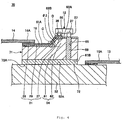
- Fig. 3 is a sectional view illustrating a light-emitting device according to a second embodiment of the invention.
- the light-emitting device 50 has external connection leads 14 and 15, a wiring substrate 51, a heat-sinking plate 52 and a light-emitting element 12.
- the wiring substrate 51 has a substrate body 54, an insulation layer 18, a first wiring pattern 21 and a penetrating electrode 55.
- the substrate body 54 has a substrate portion 61 and a protruding portion 62.
- the protruding portion 62 is integrated into the substrate portion 61.
- the protruding portion 62 is disposed on the top surface 61A of the substrate portion 61 and protrudes from the top surface 61A of the substrate portion 61.
- the top surface 62A of the protruding portion 62 protrudes higher than the top surface 14A of a portion of the external connection lead, the portion disposed on the first wiring pattern 21.
- the protruding portion 62 serves to enable the light-emitting element 12 to protrude higher than the top surface 14A of the portion of the external connection lead 14, the portion disposed on the first wiring pattern 21.
- a Height H2 (height measured when the top surface 61A of the substrate portion 61 is a base level) of the protruding portion 62 may be about 400 ⁇ m.
- the protruding portion 62 which enables the light-emitting element 12 to protrude higher than the top surface 14A of the portion of the external connection lead 14.
- the sub-mount substrate 102 (see Fig. 1 ) provided in the related-art light-emitting device 100 becomes unnecessary. Accordingly, it is possible to effectively use light emitted from the entire surface of the light-emitting element 12. Further, in the light-emitting device 50, since there is no necessity to use two substrates (the sub-mount substrate 102 and the board substrate 103) unlike the conventional light-emitting device 100 but a single wiring substrate 51 is enough to use, the cost of the light-emitting device 50 can be reduced.
- the protruding portion 62 has a side surface 62B on which the insulation layer 18 is formed.
- the side surface 62B of the protruding portion 62 is an inclined surface inclined at an angle of ⁇ 2 with respect to the top surface 61A of the substrate portion 61.
- the angle ⁇ 2 can be, for example, 54.7° or 90°.
- the substrate body 51 has a penetrating hole 65 which penetrates the protruding portion 62 and the substrate portion 61 disposed under the protruding portion 62.
- a material for the substrate body 54 can be silicon.
- An advantage of using silicon as a material for the substrate body 54 is that it is easy to form the protruding portion 62 having the inclined side surface 62B.
- the insulation layer 18 covers the top surface 61A of the substrate portion 61 and the top surface 62A and the side surface 62B of the protruding portion 62.
- the insulation layer 18 is a layer for electrically insulating the first wiring pattern 21 from the penetrating electrode 55.
- the first wiring pattern 21 includes a light-emitting element connection pad 27, a lead connection portion 28 and a wiring portion 29.
- the light-emitting element connection pad 27 is disposed on the insulation layer 18 formed on the protruding portion 62.
- the light-emitting element connection pad 27 is electrically connected to the first power supply terminal 36 of the light-emitting element 12 via a bump 56.
- the lead connection portion 28 is disposed on the insulation layer 18 formed on the top surface 61A of the substrate portion 61.
- the lead connection portion 28 is electrically connected to the external connection lead 14.
- the wiring portion 29 is disposed on the insulation layer 18 formed on the side surface 62B of the protruding portion 62 and the top surface 61A of the substrate portion 61.
- the wiring portion 29 is connected to the light-emitting element connection pad 27 at an end thereof and to the lead connection portion 28 at the other end thereof.
- the wiring portion 29 serves to electrically connect the light-emitting element connection pad 27 with the lead connection portion 28.
- the penetrating electrode 55 is formed in the penetrating hole 65.
- a top end portion of the penetrating electrode 55 and the top surface 18A of the insulation layer 18 are in almost the same plane.
- the top end portion of the penetrating electrode 55 is electrically connected to the second power supply terminal of the light-emitting element 12 via a bump 57.
- a bottom end portion of the penetrating electrode 55 and the bottom surface61B of the substrate portion 61 are in almost the same plane.
- the bottom end portion of the penetrating electrode 55 is electrically and thermally connected to the heat-sinking plate 52 having electrical conductivity by using Ag paste as an adhesive.
- the penetrating electrode 55 is preferably made of a material having thermal conductivity higher than silicon and having electrical conductivity. In detail, it is possible to use copper Cu as the material for the penetrating electrode 55.
- the penetrating electrode can be manufactured, for example by using a plating method.
- the size of the substrate body 54 can be reduced. As a result, the cost of the light-emitting device 50 can be reduced.
- the penetrating electrode 55 is formed of as a material having thermal conductivity higher silicon and having electrical conductivity, it is possible to effectively transmit heat generated when the light-emitting element 12 emits light to the heat-sinking plate 52.
- the heat-sinking plate 52 is attached to the bottom surface 51B of the wiring substrate 51 by using Ag paste as an adhesive.
- the heat-sinking plate 52 is preferably made of a material having electrical conductivity and high thermal conductivity.
- a material for the heat-sinking plate 52 can be copper Cu which has high thermal conductivity.
- the heat-sinking plate 52 is made of a conductive material, it is possible to electrically connect the penetrating electrode 55 with the external connection lead 15.
- the heat-sinking plate 52 is made of a material having electrical conductivity and high thermal conductivity, it is possible to enhance heat-sinking efficiency of the heat-sinking plate 52.
- the external connection lead 14 is attached to the lead connection portion 28 by using Ag paste as an adhesive. Thanks to such configuration, the external connection lead 14 can be electrically connected to the first power supply terminal 36 via the first wiring pattern 21.
- the external connection lead 15 is attached to the heat-sinking plate 52 by using Ag paste as an adhesive. Thanks to such configuration, the external connection lead 15 is electrically connected to the second power supply terminal 37 via the heat-sinking plate 52 and the penetrating electrode 55.
- the light-emitting element 12 is disposed at the position higher than the top surface 14A of the external connection lead 14 formed on the first wiring pattern 21. Thanks to such configuration in which the light-emitting element 12 is disposed at the position higher than the top surface 14A of the external connection lead 14 formed on the first wiring pattern 21, it is possible to effectively use light emitted from the entire surface of the light-emitting element 12.
- the light-emitting element 12 includes the first power supply terminal 36 and the second power supply terminal 37.
- the first power supply terminal 36 is electrically connected to the light-emitting element connection pad 27 via the bump 56.
- the second power supply terminal 37 is electrically connected to the penetrating electrode 55 via the bump 57.
- the penetrating electrode 55 which penetrates the protruding portion 62 and the substrate portion 61 disposed under the protruding portion 62 is provided and the penetrating electrode 55 and the second power supply terminal 37 are electrically connected. It is therefore possible to reduce the size of the substrate body 54, resulting in cost reduction of the light-emitting device 50.
- the penetrating electrode 55 is made of a material having electrical conductivity and thermal conductivity higher than silicon, it is therefore possible to effectively transmit the heat generated when the light-emitting element 12 emits light to the heat-sinking plate 52.
- the light-emitting device 50 according to this embodiment can attain the same advantages as the light-emitting device 10 according to the first embodiment.
- Ag paste is used as an adhesive in the light-emitting device 50 according to this embodiment
- another adhesives can be also used as long as they are electrically conductive.
- Ag paste is used in the light-emitting device 50 according to this embodiment in order to make connections between the external connection lead 14 and the first wiring pattern 21 and between the external connection lead 15 and the heat-sinking plate 52
- such connections can be realized in an alternative manner. That is, the external connection lead 14 and the first wiring pattern 21 may be electrically connected and the external connection lead 15 and the heat-sinking plate 52 may be made electrically connected, without using a conductive adhesive such as Ag paste.
- the wiring substrate 51 and the heat-sinking plate 52 are placed in a casing, a frame-shaped body designed to expose the light-emitting element 12 is pressed against the external connection leads 14 and 15, and the frame body is held by the casing.
- Fig. 4 is a sectional view illustrating a light-emitting device according to a third embodiment of the invention.
- a light-emitting device 70 according to the third embodiment of the invention is configured in the same manner as the light-emitting device 50 according to the second embodiment, except one thing that the wiring substrate 51 in the second embodiment is substituted with a wiring substrate 71.
- the wiring substrate 71 is configured in the same manner as the wiring substrate 51 explained with reference to the second embodiment, except one thing that the wiring substrate 71 additionally includes a metal layer in.
- the metal layer 72 is made of a metal having high thermal conductivity.
- the metal layer 72 is formed on the bottom surface 61B of a substrate portion 61.
- the metal layer 72 is connected to a lower end portion of a penetrating electrode 55. Thanks to such configuration, the metal layer 72 is electrically and thermally connected to a second power supply terminal 37 via the penetrating electrode 55.
- the metal layer is fixed to the heat-sinking plate 52 by using Ag paste as an adhesive. That is, the metal layer 72 is disposed between the substrate portion 61 and the heat-sinking plate 52. Thanks to such configuration, the heat-sinking plate is electrically and thermally connected to the second power supply terminal of the light-emitting element 12.
- the metal layer 72 can be made of copper Cu.
- the metal layer 72 can be manufactured for example by using a plating method.
- a thickness of the metal layer may be about 5 ⁇ m.
- the metal layer 72 having high thermal conductivity and connected to the penetrating electrode 55 is provided between the substrate portion 61 and the heat-sinking plate 52. It is therefore possible to transmit the heat generated when the light-emitting element 12 emits light to the heat-sinking plate 51, so that heat-sinking efficiency can be enhanced.
- the metal layer 72 is fixed to the heat-sinking plate 52 using Ag paste as an adhesive
- the metal layer may be fixed to the heat-sinking plate 52 by using a direct bonding method without using Ag paste.
- the direct bonding method the bottom surface 72A of the metal layer 72 and the top surface 52A of the heat-sinking plate are activated by plasma to be smooth and flat, then the bottom surface72A of the metal layer 72 is pressed against the top surface 52A of the heat-sinking plate 52, and finally the metal layer 72 and the heat-sinking plate 52 are bonded.
- the metal layer 72 and the heat-sinking plate 52 may be heated so as to be bonded.
- Ag paste is used as an adhesive in the light-emitting device 70 according to this embodiment
- another adhesives also may be used as long as they are electrically conductive.
- the external connection lead 14 and the first wiring pattern 21 may be electrically connected and also the external connection lead 15 and the heat-sinking plate 52 may be electrically connected without using a conductive adhesive such as Ag paste.
- the wiring substrate 71 and the heat-sinking plate 52 are placed in a casing, a frame body designed to expose the light-emitting element 12 is pressed against the external connection leads 14 and 15, and the frame body is held by the casing.
- the invention can be applied to light-emitting devices which can effectively use light emitted from the entire surface of light-emitting elements and can reduce the cost thereof.
Landscapes
- Led Device Packages (AREA)
Applications Claiming Priority (1)
| Application Number | Priority Date | Filing Date | Title |
|---|---|---|---|
| JP2006214700A JP5214121B2 (ja) | 2006-08-07 | 2006-08-07 | 発光装置 |
Publications (3)
| Publication Number | Publication Date |
|---|---|
| EP1887635A2 EP1887635A2 (en) | 2008-02-13 |
| EP1887635A3 EP1887635A3 (en) | 2012-12-26 |
| EP1887635B1 true EP1887635B1 (en) | 2017-05-10 |
Family
ID=38657872
Family Applications (1)
| Application Number | Title | Priority Date | Filing Date |
|---|---|---|---|
| EP07015539.5A Active EP1887635B1 (en) | 2006-08-07 | 2007-08-07 | Light-emitting device |
Country Status (4)
| Country | Link |
|---|---|
| US (1) | US7816690B2 (enExample) |
| EP (1) | EP1887635B1 (enExample) |
| JP (1) | JP5214121B2 (enExample) |
| TW (1) | TW200810160A (enExample) |
Families Citing this family (6)
| Publication number | Priority date | Publication date | Assignee | Title |
|---|---|---|---|---|
| TWI353657B (en) * | 2007-09-28 | 2011-12-01 | Ind Tech Res Inst | An island submount |
| CN102881812B (zh) * | 2011-07-15 | 2015-03-25 | 赛恩倍吉科技顾问(深圳)有限公司 | 发光二极管封装结构的制造方法 |
| JP6006525B2 (ja) * | 2012-05-15 | 2016-10-12 | スタンレー電気株式会社 | 半導体発光装置及びそれを用いた灯具 |
| KR101978941B1 (ko) * | 2013-01-28 | 2019-05-15 | 엘지이노텍 주식회사 | 발광소자 패키지 |
| KR102153041B1 (ko) * | 2013-12-04 | 2020-09-07 | 삼성전자주식회사 | 반도체소자 패키지 및 그 제조방법 |
| JP7311595B2 (ja) * | 2019-06-11 | 2023-07-19 | 京セラ株式会社 | 発光素子基板および表示装置、ならびに表示装置の製造方法 |
Family Cites Families (20)
| Publication number | Priority date | Publication date | Assignee | Title |
|---|---|---|---|---|
| JPS54389B2 (enExample) * | 1975-05-06 | 1979-01-10 | ||
| JPH0513820A (ja) * | 1991-07-02 | 1993-01-22 | Omron Corp | 半導体装置 |
| DE4242842C2 (de) * | 1992-02-14 | 1999-11-04 | Sharp Kk | Lichtemittierendes Bauelement zur Oberflächenmontage und Verfahren zu dessen Herstellung |
| DE10006738C2 (de) * | 2000-02-15 | 2002-01-17 | Osram Opto Semiconductors Gmbh | Lichtemittierendes Bauelement mit verbesserter Lichtauskopplung und Verfahren zu seiner Herstellung |
| US6600231B2 (en) * | 2000-05-11 | 2003-07-29 | Mitutoyo Corporation | Functional device unit and method of producing the same |
| DE10163799B4 (de) * | 2000-12-28 | 2006-11-23 | Matsushita Electric Works, Ltd., Kadoma | Halbleiterchip-Aufbausubstrat und Verfahren zum Herstellen eines solchen Aufbausubstrates |
| DE10105802A1 (de) * | 2001-02-07 | 2002-08-08 | Patent Treuhand Ges Fuer Elektrische Gluehlampen Mbh | Reflektorbehaftetes Halbleiterbauelement |
| JP2003031895A (ja) * | 2001-07-13 | 2003-01-31 | Sharp Corp | 半導体発光装置およびその製造方法 |
| JP4045781B2 (ja) * | 2001-08-28 | 2008-02-13 | 松下電工株式会社 | 発光装置 |
| DE10148227B4 (de) * | 2001-09-28 | 2015-03-05 | Osram Opto Semiconductors Gmbh | Strahlungsemittierender Halbleiterchip, Verfahren zu dessen Herstellung und strahlungsemittierendes Bauelement |
| CN100338786C (zh) * | 2002-06-19 | 2007-09-19 | 三垦电气株式会社 | 半导体发光装置及其制法和半导体发光装置用反射器 |
| JP3993475B2 (ja) * | 2002-06-20 | 2007-10-17 | ローム株式会社 | Ledチップの実装構造、およびこれを備えた画像読み取り装置 |
| CN100587560C (zh) * | 2003-04-01 | 2010-02-03 | 夏普株式会社 | 发光装置用组件、发光装置、背侧光照射装置、显示装置 |
| JP4192742B2 (ja) * | 2003-09-30 | 2008-12-10 | 豊田合成株式会社 | 発光装置 |
| JP2005136224A (ja) * | 2003-10-30 | 2005-05-26 | Asahi Kasei Electronics Co Ltd | 発光ダイオード照明モジュール |
| TWI227570B (en) * | 2003-12-11 | 2005-02-01 | South Epitaxy Corp | Light-emitting diode packaging structure |
| JP2005203448A (ja) | 2004-01-13 | 2005-07-28 | Toyoda Gosei Co Ltd | 発光装置 |
| JP4614679B2 (ja) | 2004-01-29 | 2011-01-19 | 京セラ株式会社 | 発光装置およびその製造方法ならびに照明装置 |
| JP2006135276A (ja) * | 2004-10-04 | 2006-05-25 | Hitachi Ltd | 半導体発光素子搭載用パッケージ及びその製造方法 |
| JP2006324324A (ja) * | 2005-05-17 | 2006-11-30 | Sumitomo Electric Ind Ltd | 発光装置、発光装置の製造方法および窒化物半導体基板 |
-
2006
- 2006-08-07 JP JP2006214700A patent/JP5214121B2/ja active Active
-
2007
- 2007-08-06 US US11/882,812 patent/US7816690B2/en active Active
- 2007-08-07 TW TW096128945A patent/TW200810160A/zh unknown
- 2007-08-07 EP EP07015539.5A patent/EP1887635B1/en active Active
Also Published As
| Publication number | Publication date |
|---|---|
| EP1887635A3 (en) | 2012-12-26 |
| US7816690B2 (en) | 2010-10-19 |
| EP1887635A2 (en) | 2008-02-13 |
| JP5214121B2 (ja) | 2013-06-19 |
| JP2008041953A (ja) | 2008-02-21 |
| TW200810160A (en) | 2008-02-16 |
| US20080030139A1 (en) | 2008-02-07 |
Similar Documents
| Publication | Publication Date | Title |
|---|---|---|
| TWI235469B (en) | Thermally enhanced semiconductor package with EMI shielding | |
| KR101095291B1 (ko) | 고온 동작을 위한 패키징된 발광 다이오드들 | |
| US8916958B2 (en) | Semiconductor package with multiple chips and substrate in metal cap | |
| CN102148316B (zh) | 采用电表面安装的发光晶片封装 | |
| JP4841836B2 (ja) | フリップチップ式発光ダイオードの発光装置製造方法 | |
| EP3602626B1 (en) | Lighting device with led elements on a mounting element on a flat carrier and method of manufacturing the same | |
| US20060006405A1 (en) | Surface mountable light emitting diode assemblies packaged for high temperature operation | |
| US20090174044A1 (en) | Multi-chip package | |
| US20100059783A1 (en) | Light Emitting Chip Package With Metal Leads For Enhanced Heat Dissipation | |
| CN101292360A (zh) | 可用于多芯片模块中的用于热应力释放的集成电路安装 | |
| JP2006525679A5 (enExample) | ||
| EP1466357B1 (en) | Surface mounted package with die bottom spaced from support board | |
| EP1887635B1 (en) | Light-emitting device | |
| US7176563B2 (en) | Electronically grounded heat spreader | |
| JP2013532894A (ja) | オプトエレクトロニクス発光モジュール及び自動車用ヘッドライト | |
| EP2852975B1 (en) | Surface mountable semiconductor device | |
| JP2006073699A (ja) | 発光素子収納用パッケージ | |
| JP2015046495A (ja) | 発光素子搭載用基板および発光装置 | |
| US8237188B2 (en) | Light source | |
| JP2008504711A (ja) | 発光ダイオードモジュール | |
| JP5912471B2 (ja) | 半導体デバイス | |
| US7310224B2 (en) | Electronic apparatus with thermal module | |
| JPS63190363A (ja) | パワ−パツケ−ジ | |
| JP4797621B2 (ja) | 半導体装置およびその製造方法 | |
| KR100638881B1 (ko) | 금속 기판에 led 패키지를 삽입한 led 어셈블리 |
Legal Events
| Date | Code | Title | Description |
|---|---|---|---|
| PUAI | Public reference made under article 153(3) epc to a published international application that has entered the european phase |
Free format text: ORIGINAL CODE: 0009012 |
|
| AK | Designated contracting states |
Kind code of ref document: A2 Designated state(s): AT BE BG CH CY CZ DE DK EE ES FI FR GB GR HU IE IS IT LI LT LU LV MC MT NL PL PT RO SE SI SK TR |
|
| AX | Request for extension of the european patent |
Extension state: AL BA HR MK YU |
|
| PUAL | Search report despatched |
Free format text: ORIGINAL CODE: 0009013 |
|
| AK | Designated contracting states |
Kind code of ref document: A3 Designated state(s): AT BE BG CH CY CZ DE DK EE ES FI FR GB GR HU IE IS IT LI LT LU LV MC MT NL PL PT RO SE SI SK TR |
|
| AX | Request for extension of the european patent |
Extension state: AL BA HR MK RS |
|
| RIC1 | Information provided on ipc code assigned before grant |
Ipc: H01L 33/62 20100101AFI20121119BHEP Ipc: H01L 33/48 20100101ALN20121119BHEP |
|
| 17P | Request for examination filed |
Effective date: 20130626 |
|
| RBV | Designated contracting states (corrected) |
Designated state(s): AT BE BG CH CY CZ DE DK EE ES FI FR GB GR HU IE IS IT LI LT LU LV MC MT NL PL PT RO SE SI SK TR |
|
| RBV | Designated contracting states (corrected) |
Designated state(s): AT BE BG CH CY CZ DE DK EE ES FI FR GB GR HU IE IS IT LI LT LU LV MC MT NL PL PT RO SE SI SK TR |
|
| RBV | Designated contracting states (corrected) |
Designated state(s): AT BE BG CH CY CZ DE DK EE ES FI FR GB GR HU IE IS IT LI LT LU LV MC MT NL PL PT RO SE SI SK TR |
|
| REG | Reference to a national code |
Ref country code: DE Ref legal event code: R079 Ref document number: 602007050904 Country of ref document: DE Free format text: PREVIOUS MAIN CLASS: H01L0033000000 Ipc: H01L0033620000 |
|
| GRAP | Despatch of communication of intention to grant a patent |
Free format text: ORIGINAL CODE: EPIDOSNIGR1 |
|
| RIC1 | Information provided on ipc code assigned before grant |
Ipc: H01L 33/48 20100101ALN20161128BHEP Ipc: H01L 33/62 20100101AFI20161128BHEP |
|
| INTG | Intention to grant announced |
Effective date: 20161213 |
|
| GRAS | Grant fee paid |
Free format text: ORIGINAL CODE: EPIDOSNIGR3 |
|
| GRAA | (expected) grant |
Free format text: ORIGINAL CODE: 0009210 |
|
| AK | Designated contracting states |
Kind code of ref document: B1 Designated state(s): AT BE BG CH CY CZ DE DK EE ES FI FR GB GR HU IE IS IT LI LT LU LV MC MT NL PL PT RO SE SI SK TR |
|
| REG | Reference to a national code |
Ref country code: GB Ref legal event code: FG4D |
|
| REG | Reference to a national code |
Ref country code: AT Ref legal event code: REF Ref document number: 893159 Country of ref document: AT Kind code of ref document: T Effective date: 20170515 Ref country code: CH Ref legal event code: EP |
|
| REG | Reference to a national code |
Ref country code: IE Ref legal event code: FG4D |
|
| REG | Reference to a national code |
Ref country code: DE Ref legal event code: R096 Ref document number: 602007050904 Country of ref document: DE |
|
| REG | Reference to a national code |
Ref country code: NL Ref legal event code: MP Effective date: 20170510 |
|
| REG | Reference to a national code |
Ref country code: LT Ref legal event code: MG4D |
|
| REG | Reference to a national code |
Ref country code: AT Ref legal event code: MK05 Ref document number: 893159 Country of ref document: AT Kind code of ref document: T Effective date: 20170510 |
|
| PG25 | Lapsed in a contracting state [announced via postgrant information from national office to epo] |
Ref country code: ES Free format text: LAPSE BECAUSE OF FAILURE TO SUBMIT A TRANSLATION OF THE DESCRIPTION OR TO PAY THE FEE WITHIN THE PRESCRIBED TIME-LIMIT Effective date: 20170510 Ref country code: LT Free format text: LAPSE BECAUSE OF FAILURE TO SUBMIT A TRANSLATION OF THE DESCRIPTION OR TO PAY THE FEE WITHIN THE PRESCRIBED TIME-LIMIT Effective date: 20170510 Ref country code: FI Free format text: LAPSE BECAUSE OF FAILURE TO SUBMIT A TRANSLATION OF THE DESCRIPTION OR TO PAY THE FEE WITHIN THE PRESCRIBED TIME-LIMIT Effective date: 20170510 Ref country code: AT Free format text: LAPSE BECAUSE OF FAILURE TO SUBMIT A TRANSLATION OF THE DESCRIPTION OR TO PAY THE FEE WITHIN THE PRESCRIBED TIME-LIMIT Effective date: 20170510 Ref country code: GR Free format text: LAPSE BECAUSE OF FAILURE TO SUBMIT A TRANSLATION OF THE DESCRIPTION OR TO PAY THE FEE WITHIN THE PRESCRIBED TIME-LIMIT Effective date: 20170811 |
|
| PG25 | Lapsed in a contracting state [announced via postgrant information from national office to epo] |
Ref country code: LV Free format text: LAPSE BECAUSE OF FAILURE TO SUBMIT A TRANSLATION OF THE DESCRIPTION OR TO PAY THE FEE WITHIN THE PRESCRIBED TIME-LIMIT Effective date: 20170510 Ref country code: BG Free format text: LAPSE BECAUSE OF FAILURE TO SUBMIT A TRANSLATION OF THE DESCRIPTION OR TO PAY THE FEE WITHIN THE PRESCRIBED TIME-LIMIT Effective date: 20170810 Ref country code: SE Free format text: LAPSE BECAUSE OF FAILURE TO SUBMIT A TRANSLATION OF THE DESCRIPTION OR TO PAY THE FEE WITHIN THE PRESCRIBED TIME-LIMIT Effective date: 20170510 Ref country code: PL Free format text: LAPSE BECAUSE OF FAILURE TO SUBMIT A TRANSLATION OF THE DESCRIPTION OR TO PAY THE FEE WITHIN THE PRESCRIBED TIME-LIMIT Effective date: 20170510 Ref country code: NL Free format text: LAPSE BECAUSE OF FAILURE TO SUBMIT A TRANSLATION OF THE DESCRIPTION OR TO PAY THE FEE WITHIN THE PRESCRIBED TIME-LIMIT Effective date: 20170510 Ref country code: IS Free format text: LAPSE BECAUSE OF FAILURE TO SUBMIT A TRANSLATION OF THE DESCRIPTION OR TO PAY THE FEE WITHIN THE PRESCRIBED TIME-LIMIT Effective date: 20170910 |
|
| PG25 | Lapsed in a contracting state [announced via postgrant information from national office to epo] |
Ref country code: EE Free format text: LAPSE BECAUSE OF FAILURE TO SUBMIT A TRANSLATION OF THE DESCRIPTION OR TO PAY THE FEE WITHIN THE PRESCRIBED TIME-LIMIT Effective date: 20170510 Ref country code: SK Free format text: LAPSE BECAUSE OF FAILURE TO SUBMIT A TRANSLATION OF THE DESCRIPTION OR TO PAY THE FEE WITHIN THE PRESCRIBED TIME-LIMIT Effective date: 20170510 Ref country code: CZ Free format text: LAPSE BECAUSE OF FAILURE TO SUBMIT A TRANSLATION OF THE DESCRIPTION OR TO PAY THE FEE WITHIN THE PRESCRIBED TIME-LIMIT Effective date: 20170510 Ref country code: DK Free format text: LAPSE BECAUSE OF FAILURE TO SUBMIT A TRANSLATION OF THE DESCRIPTION OR TO PAY THE FEE WITHIN THE PRESCRIBED TIME-LIMIT Effective date: 20170510 Ref country code: RO Free format text: LAPSE BECAUSE OF FAILURE TO SUBMIT A TRANSLATION OF THE DESCRIPTION OR TO PAY THE FEE WITHIN THE PRESCRIBED TIME-LIMIT Effective date: 20170510 |
|
| REG | Reference to a national code |
Ref country code: DE Ref legal event code: R097 Ref document number: 602007050904 Country of ref document: DE |
|
| PG25 | Lapsed in a contracting state [announced via postgrant information from national office to epo] |
Ref country code: IT Free format text: LAPSE BECAUSE OF FAILURE TO SUBMIT A TRANSLATION OF THE DESCRIPTION OR TO PAY THE FEE WITHIN THE PRESCRIBED TIME-LIMIT Effective date: 20170510 |
|
| PLBE | No opposition filed within time limit |
Free format text: ORIGINAL CODE: 0009261 |
|
| STAA | Information on the status of an ep patent application or granted ep patent |
Free format text: STATUS: NO OPPOSITION FILED WITHIN TIME LIMIT |
|
| REG | Reference to a national code |
Ref country code: CH Ref legal event code: PL |
|
| PG25 | Lapsed in a contracting state [announced via postgrant information from national office to epo] |
Ref country code: MC Free format text: LAPSE BECAUSE OF FAILURE TO SUBMIT A TRANSLATION OF THE DESCRIPTION OR TO PAY THE FEE WITHIN THE PRESCRIBED TIME-LIMIT Effective date: 20170510 |
|
| 26N | No opposition filed |
Effective date: 20180213 |
|
| GBPC | Gb: european patent ceased through non-payment of renewal fee |
Effective date: 20170810 |
|
| PG25 | Lapsed in a contracting state [announced via postgrant information from national office to epo] |
Ref country code: CH Free format text: LAPSE BECAUSE OF NON-PAYMENT OF DUE FEES Effective date: 20170831 Ref country code: LI Free format text: LAPSE BECAUSE OF NON-PAYMENT OF DUE FEES Effective date: 20170831 |
|
| REG | Reference to a national code |
Ref country code: FR Ref legal event code: ST Effective date: 20180430 |
|
| REG | Reference to a national code |
Ref country code: IE Ref legal event code: MM4A |
|
| PG25 | Lapsed in a contracting state [announced via postgrant information from national office to epo] |
Ref country code: SI Free format text: LAPSE BECAUSE OF FAILURE TO SUBMIT A TRANSLATION OF THE DESCRIPTION OR TO PAY THE FEE WITHIN THE PRESCRIBED TIME-LIMIT Effective date: 20170510 |
|
| REG | Reference to a national code |
Ref country code: BE Ref legal event code: MM Effective date: 20170831 |
|
| PG25 | Lapsed in a contracting state [announced via postgrant information from national office to epo] |
Ref country code: LU Free format text: LAPSE BECAUSE OF NON-PAYMENT OF DUE FEES Effective date: 20170807 |
|
| PG25 | Lapsed in a contracting state [announced via postgrant information from national office to epo] |
Ref country code: IE Free format text: LAPSE BECAUSE OF NON-PAYMENT OF DUE FEES Effective date: 20170807 Ref country code: GB Free format text: LAPSE BECAUSE OF NON-PAYMENT OF DUE FEES Effective date: 20170810 |
|
| PG25 | Lapsed in a contracting state [announced via postgrant information from national office to epo] |
Ref country code: FR Free format text: LAPSE BECAUSE OF NON-PAYMENT OF DUE FEES Effective date: 20170831 Ref country code: BE Free format text: LAPSE BECAUSE OF NON-PAYMENT OF DUE FEES Effective date: 20170831 |
|
| PG25 | Lapsed in a contracting state [announced via postgrant information from national office to epo] |
Ref country code: MT Free format text: LAPSE BECAUSE OF NON-PAYMENT OF DUE FEES Effective date: 20170807 |
|
| PG25 | Lapsed in a contracting state [announced via postgrant information from national office to epo] |
Ref country code: HU Free format text: LAPSE BECAUSE OF FAILURE TO SUBMIT A TRANSLATION OF THE DESCRIPTION OR TO PAY THE FEE WITHIN THE PRESCRIBED TIME-LIMIT; INVALID AB INITIO Effective date: 20070807 |
|
| PG25 | Lapsed in a contracting state [announced via postgrant information from national office to epo] |
Ref country code: CY Free format text: LAPSE BECAUSE OF NON-PAYMENT OF DUE FEES Effective date: 20170510 |
|
| PG25 | Lapsed in a contracting state [announced via postgrant information from national office to epo] |
Ref country code: TR Free format text: LAPSE BECAUSE OF FAILURE TO SUBMIT A TRANSLATION OF THE DESCRIPTION OR TO PAY THE FEE WITHIN THE PRESCRIBED TIME-LIMIT Effective date: 20170510 |
|
| PG25 | Lapsed in a contracting state [announced via postgrant information from national office to epo] |
Ref country code: PT Free format text: LAPSE BECAUSE OF FAILURE TO SUBMIT A TRANSLATION OF THE DESCRIPTION OR TO PAY THE FEE WITHIN THE PRESCRIBED TIME-LIMIT Effective date: 20170510 |
|
| REG | Reference to a national code |
Ref country code: DE Ref legal event code: R079 Ref document number: 602007050904 Country of ref document: DE Free format text: PREVIOUS MAIN CLASS: H01L0033620000 Ipc: H10H0020857000 |
|
| PGFP | Annual fee paid to national office [announced via postgrant information from national office to epo] |
Ref country code: DE Payment date: 20250702 Year of fee payment: 19 |