EP1835261A2 - Verfahren und Schaltung zur Korrektur von temperaturabhängigen Sensoreigenschaften - Google Patents
Verfahren und Schaltung zur Korrektur von temperaturabhängigen Sensoreigenschaften Download PDFInfo
- Publication number
- EP1835261A2 EP1835261A2 EP06124192A EP06124192A EP1835261A2 EP 1835261 A2 EP1835261 A2 EP 1835261A2 EP 06124192 A EP06124192 A EP 06124192A EP 06124192 A EP06124192 A EP 06124192A EP 1835261 A2 EP1835261 A2 EP 1835261A2
- Authority
- EP
- European Patent Office
- Prior art keywords
- correction
- circuit
- data
- temperature
- points
- Prior art date
- Legal status (The legal status is an assumption and is not a legal conclusion. Google has not performed a legal analysis and makes no representation as to the accuracy of the status listed.)
- Withdrawn
Links
Images





Classifications
-
- G—PHYSICS
- G01—MEASURING; TESTING
- G01D—MEASURING NOT SPECIALLY ADAPTED FOR A SPECIFIC VARIABLE; ARRANGEMENTS FOR MEASURING TWO OR MORE VARIABLES NOT COVERED IN A SINGLE OTHER SUBCLASS; TARIFF METERING APPARATUS; MEASURING OR TESTING NOT OTHERWISE PROVIDED FOR
- G01D3/00—Indicating or recording apparatus with provision for the special purposes referred to in the subgroups
- G01D3/02—Indicating or recording apparatus with provision for the special purposes referred to in the subgroups with provision for altering or correcting the law of variation
- G01D3/022—Indicating or recording apparatus with provision for the special purposes referred to in the subgroups with provision for altering or correcting the law of variation having an ideal characteristic, map or correction data stored in a digital memory
-
- G—PHYSICS
- G01—MEASURING; TESTING
- G01D—MEASURING NOT SPECIALLY ADAPTED FOR A SPECIFIC VARIABLE; ARRANGEMENTS FOR MEASURING TWO OR MORE VARIABLES NOT COVERED IN A SINGLE OTHER SUBCLASS; TARIFF METERING APPARATUS; MEASURING OR TESTING NOT OTHERWISE PROVIDED FOR
- G01D3/00—Indicating or recording apparatus with provision for the special purposes referred to in the subgroups
- G01D3/028—Indicating or recording apparatus with provision for the special purposes referred to in the subgroups mitigating undesired influences, e.g. temperature, pressure
- G01D3/036—Indicating or recording apparatus with provision for the special purposes referred to in the subgroups mitigating undesired influences, e.g. temperature, pressure on measuring arrangements themselves
- G01D3/0365—Indicating or recording apparatus with provision for the special purposes referred to in the subgroups mitigating undesired influences, e.g. temperature, pressure on measuring arrangements themselves the undesired influence being measured using a separate sensor, which produces an influence related signal
Definitions
- the present invention relates to a method and circuit for correcting an output signal of a sensor, such as an angular velocity sensor or an acceleration sensor.
- Sensors have been miniaturized over recent years and have finer output signals.
- Such a sensor requires an amplification circuit for detecting and amplifying sensor output. Output signals from the sensor and the amplification circuit are dependent on temperature. Thus, the amplification circuit is required to correct such temperature dependent characteristics. Accordingly, there is a need for performing such a correction process accurately and easily.
- a digital correction process and an analog correction process have been employed by sensor amplification circuits to correct the temperature dependent characteristic of a sensor output.
- the digital correction process uses correction data prestored for every predetermined temperature step in a storage means.
- the amplification circuit reads correction data corresponding to an ambient temperature from the storage means and generates an output signal by correcting the sensor output based on the correction data.
- a gradient is set for the temperature characteristic of the amplification circuit to offset the predetermined gradient of the sensor output.
- the sensor output changes along a curve with respect to temperature changes, the sensor output is approximated with a plurality of straight lines to switch the gradient of the temperature dependent characteristic of the amplification circuit in accordance with the temperature. In this way, the amplification circuit corrects the sensor output to generate the output signal.
- Fig. 1 is a schematic block circuit diagram of a conventional sensor amplification circuit 2 including a digital correction function.
- the amplification circuit 2 is formed by an IC chip and connected to a bridge type sensor 1.
- the amplification circuit 2 includes an amplification circuit unit 4 for amplifying the output of the sensor 1 and generating an output signal Vout.
- the amplification circuit unit 4 includes a digital correction function for correcting the output of the sensor 1 in a digital manner.
- the sensor 1 is supplied with constant current from a current source 3 in the amplification circuit 2. Output voltages Vs1 and Vs2 of the sensor 1 are supplied to the amplification circuit unit 4.
- the amplification circuit unit 4 includes input-stage amplifiers 5a and 5b for receiving the output voltages Vs1 and Vs2 of the sensor 1, an amplifier 6 for amplifying the difference between output voltages of the input-stage amplifiers 5a and 5b, an amplifier 7 for amplifying an output signal of the amplifier 6, and an output-stage amplifier 8 for amplifying an output voltage of the amplifier 7.
- the input-stage amplifiers 5a and 5b is respectively connected to the feedback resistors R1a and R1b, which are variable resistors.
- the resistances of the feedback resistors R1a and R1b are adjusted to adjust the gain of the amplification circuit unit 4.
- the amplifier 6 includes two input terminals, one of which is connected to ground GND via a voltage adjustment circuit 9.
- the voltage adjustment circuit 9 has a voltage that is adjusted to adjust the offset voltage of the amplification circuit unit 4.
- the amplifier 7 is connected to a feedback resistor R2, which is a variable resistor.
- the resistance of the feedback resistor R2 is adjusted to adjust the gain of the amplification circuit unit 4.
- the output-stage amplifier 8 includes two input terminals, one of which is connected to ground GND via a voltage adjustment circuit 10.
- the voltage adjustment circuit 10 has a voltage that is adjusted to adjust the offset voltage of the amplification circuit unit 4.
- Each of the resistors R1a, R1b, and R2 includes a plurality of resistors connected in series and a plurality of switches respectively connected in parallel to the resistors. The switches for each of the resistors R1a, R1b, and R2 are controlled to adjust the resistance of each of the resistors R1a, R1b, and R2 in steps.
- Each of the voltage adjustment circuits 9 and 10 includes a plurality of resistors connected in series and a plurality of switches respectively connected in parallel to the resistors. The switches for each of the voltage adjustment circuits 9 and 10 are controlled to adjust the voltage in steps for each of the voltage adjustment circuits 9 and 10.
- the amplification circuit unit 4 digitally corrects the temperature characteristic of the sensor 1 in accordance with the operation of a control circuit 11.
- the amplification circuit unit 4 amplifies the output of the sensor 1 to generate an output signal Vout, which is not dependent on the temperature.
- the control circuit 11 is connected to a temperature sensor 12 and a memory device 13a.
- the temperature sensor 12 detects the ambient temperature.
- the memory device 13a prestores correction data for adjusting the resistances of the resistors R1a, R1b, and R2 and the voltage adjustment circuits 9 and 10 in accordance with the temperature detected by the temperature sensor 12.
- the control circuit 11 reads correction data corresponding to the ambient temperature from the memory device 13a based on a detection signal from the temperature sensor 12.
- the memory device 13a converts the correction data into control data and stores the control data in a data latch unit 13b.
- the resistances of the resistors R1a, R1b, and R2 and the voltage adjustment circuits 9 and 10 are adjusted based on the control data stored in the data latch unit 13b.
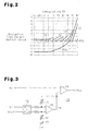
- Fig. 2 is a graph schematically showing the output characteristic of the sensor amplification circuit 2.
- Characteristic curve X1 indicates the output characteristic of the amplification circuit unit 4 when digital correction is not performed. As shown in Fig. 2, the characteristic curve X1 increases as the temperature increases. However, it is preferable that the characteristic curve X1 be corrected in a manner that the temperature characteristic is flat at a predetermined target value (zero level in Fig. 2) regardless of the temperature.
- Characteristic curve X2 indicates the output characteristic of the amplification circuit unit 4 after digital correction. As the characteristic curve X2 of Fig. 2 shows, the resistances of the resistors R1a, R1b, and R2 and the voltage adjustment circuits 9 and 10 are adjusted in intervals of 10°C at correction points P1 to P10.
- the characteristic curve X2 indicates that the level of the output signal converges on its target value at each of the correction points P1 to P10. However, the characteristic curve X2 deviates from the target value in the temperatures between the correction points P1 to P10 in accordance with the temperature dependent characteristic expressed by the characteristic curve X1. Thus, the characteristic curve X2 is plotted in a sawtooth-like manner depending on the temperature. As a result, the characteristic curve X2 is still temperature dependent and not flat.
- Fig. 3 is a schematic circuit diagram of a conventional sensor amplification circuit 20 including an analog correction function.
- An output-stage amplifier 14 includes two input terminals, one of which is supplied with output voltage Vs of a sensor and the other of which is supplied with output voltage Va of an analog correction amplifier 15.
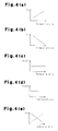
- Temperature dependent voltage Vt which is temperature dependent as shown in Fig. 4(b), and reference voltage Vref, which is not temperature dependent and constant as shown in Fig. 4(c), are respectively supplied to the two input terminals of the analog correction amplifier 15 via a switch circuit 16.
- the temperature dependent voltage Vt is generated by a forward voltage at a PN junction of a transistor or a diode.
- the temperature dependent voltage Vt changes linearly with respect to temperature changes at a gradient of, for example, - 2 mV/°C.
- the reference voltage Vref is generated using a bandgap reference voltage.
- the switch circuit 16 supplies the temperature dependent voltage Vt and the reference voltage Vref respectively to the two input terminals of the analog correction amplifier 15. If one of the input terminals of the amplifier 15 is supplied with the temperature dependent voltage Vt, the other one of the input terminals of the amplifier is supplied with the reference voltage Vref. If one of the input terminals of the amplifier 15 is supplied with the reference voltage Vref, the other one of the input terminals of the amplifier is supplied with the temperature dependent voltage Vt.
- a variable resistor R4 and a voltage adjustment circuit 17 are connected in series between the other one of the input terminals of the analog correction amplifier 15 and ground GND.
- the resistors R3 and R4 and the voltage adjustment circuit 17 are each configured in a manner similar to the resistors R1a, R1b, and R2 and the voltage adjustment circuits 9 and 10 shown in Fig. 1. Accordingly, the resistances of the resistors R3 and R4 and the voltage of the voltage adjustment circuit 17 are adjusted in steps.
- the output voltage Va of the analog correction amplifier 15 changes linearly based on changes in the ambient temperature as shown in Fig. 4(e).
- the switch circuit 16 switches the output voltage Va between the gradient of the solid line shown in Fig.4 (e) and the gradient of the broken line shown in Fig. 4(e).
- the gradient of the output voltage Va is changed by adjusting the resistances of the resistors R3 and R4.
- the offset voltage of the output signal Vout of the output-stage amplifier 14 is changed by adjusting the voltage value of the voltage adjustment circuit 17.
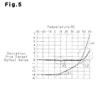
- Fig. 5 is a graph schematically showing the output characteristic of the sensor amplification circuit 20 shown in Fig. 3.
- Characteristic curve X1 shows the output characteristic of the amplifier 14 when analog correction is not performed.
- the amplification circuit 20 approximates the characteristic curve X1 from two straight lines L1 and L2 and switches the resistances of the resistors R3 and R4 and the voltage adjustment circuit 17 so as to offset the gradients and the offset values of the straight lines L1 and L2. For example, the resistances of the resistors R3 and R4 are switched at 10°C to switch from the approximate straight line L1 to the approximate straight line L2.
- the characteristic curve X3 is substantially converged to the target value (level represented by zero in Fig. 5) at temperatures in which the characteristic curve X1 coincides with the approximate straight lines L1 and L2.
- the characteristic curve X3 deviates from the target value in the vicinity of 10°C at which the switching between the approximate straight lines L1 and L2 occurs. Accordingly, a flat temperature characteristic cannot be obtained.
- Japanese Laid-Open Patent Publication No. 2003-84728 describes a voltage generation circuit that includes a circuit for performing temperature compensation through analog control and a circuit for performing temperature compensation through digital control.
- the voltage generation circuit switches between analog control and digital control in accordance with the temperature region.
- Japanese Laid-Open Patent Publication No. 11-64123 describes a bridge circuit that includes a compensation resistor for performing rough compensation for an output that changes in accordance with the temperature and a compensation unit for performing fine compensation for that output.
- Japanese Laid-Open Patent Publication No. 11-194061 describes a sensor drive circuit for performing temperature compensation in a sensor drive circuit with a digital compensation means.
- Japanese Laid-Open Patent Publication No. 2001-143183 describes a structure similar to the analog correction amplifier 15 shown in Fig. 3.
- the characteristic curve X2 digitally corrected by the sensor amplification circuit 2 shown in Figs. 1 and 2 converges on the target value at the correction points P1 to P10 that are set at intervals of 10°C but deviates from the target value between the correction points P1 to P10.
- the characteristic curve X2 changes in a sawtooth-like manner depending on the temperature.
- the characteristic curve X2 cannot show a flat temperature characteristic.
- the deviations from the target value may be reduced by increasing the correction points.
- an increase in the number of correction points increases the amount of data stored in the memory device 13a. This enlarges the memory device 13a.
- the number of times for reading correction data corresponding to each temperature from the memory device 13a increases, and the number of times the resistances are changed in the sensor amplification circuit 2 increases. This increases power supply noise and power consumption of the sensor amplification circuit 2.
- the characteristic curve X3 obtained through analog correction by the sensor amplification circuit 20 shown in Figs. 3 and 5 deviates from the target value at temperatures region in which the characteristic curve X1 deviates from the approximate straight lines L1 and Z2.
- the deviations from the target value may be reduced by increasing approximate lines.
- an increase in the number of approximate straight lines increases the number of times the resistances of the resistors R3 and R4 are changed to switch the approximate straight line gradient. This increases power supply noise and power consumption.
- the present invention provides a method and circuit for preventing an output signal, which has been corrected through digital correction and analog correction, from being deviated from a target value, while preventing power supply noise and power consumption from increasing.
- One embodiment of the present invention is a method for correcting an input signal having a temperature dependent characteristic.
- the method includes setting correction data for each of a plurality of correction points set at a predetermined temperature interval, performing a first correction for correcting the input signal with the correction data, calculating gradient data between two of the correction points that are adjacent to each other from the correction data for each of the two adjacent correction points, and performing a second correction for correcting the input signal with the gradient data.
- the correction circuit includes a memory device for storing correction data for each of a plurality of correction points set at a predetermined temperature interval.
- a first correction circuit corrects the input signal at each correction point based on the correction data corresponding to each correction point.
- a second correction circuit corrects the input signal between two of the correction points that are adjacent to each other based on gradient data calculated from the correction data for each of the two adjacent correction points.
- a sensor detects the temperature.
- a control circuit reads the correction data corresponding to the temperature detected by the temperature sensor from the memory device and controlling operation of the first correction circuit and the second correction circuit based on the correction data.
- a sensor amplification circuit 21 according to a first embodiment of the present invention will now be described with reference to Figs.6 to 10.
- Fig. 6 is a schematic block circuit diagram showing the sensor amplification circuit 21.
- the amplification circuit 21, which is formed by an IC chip, is connected to a bridge type sensor 1.
- the amplification circuit 21 has an amplification circuit unit 22.
- the amplification circuit unit 22 includes a digital correction circuit 18 (first correction circuit) for performing digital correction on a temperature dependent characteristic of an output of the sensor 1 and an analog correction circuit 19 (second correction circuit) for performing analog correction on the temperature dependent characteristic of the output of the sensor 1.
- the digital correction circuit 18 includes 5a, 5b, 6, and 7, resistors R1a, R1b, and R2, and a voltage adjustment circuit 9.
- the analog correction circuit 19 includes an amplifier 15, a switch circuit 16, a voltage adjustment circuit 17, and resistors R3 and R4.
- the bridge type sensor 1 is supplied with constant current from a current source 3 in the amplification circuit 21. Output voltages Vs1 and Vs2 of the sensor 1 are supplied to the amplification circuit unit 22 in the amplification circuit 21.
- the amplification circuit unit 22 includes input-stage amplifiers 5a and 5b for respectively receiving the output voltages Vs1 and Vs2 of the sensor 1, an amplifier 6 for amplifying the difference between output voltages of the input-stage amplifiers 5a and 5b, an amplifier 7 for amplifying an output signal of the amplifier 6, and an output-stage amplifier 8 for amplifying an output voltage of the amplifier 7.
- the amplifier 5b and 5a is respectively connected to the feedback resistors R1a and R1b, which are variable resistors.
- the resistances of the feedback resistors R1a and R1b are adjusted to adjust the gain of the amplification circuit unit 22.
- the amplifier 6 includes two input terminals, one of which is connected to ground GND via a voltage adjustment circuit 9.
- the voltage of the voltage adjustment circuit 9 is adjusted to adjust the offset voltage of the amplification circuit unit 22.
- the amplifier 7 is connected to a feedback resistor R2, which is a variable resistor.
- the resistance of the feedback resistor R2 is adjusted to adjust the gain of the amplification circuit unit 22.
- the amplifier 8 is supplied with an output signal of the amplifier 7 and an output voltage Va of an analog correction amplifier 15.
- the amplifier 8 generates an output signal Vout based on the input signals.
- each of the feedback resistors R1a, R1b, and R2 and the voltage adjustment circuit 9 includes a plurality of resistors r connected in series and a plurality of switches sw respectively connected in parallel to the resistors. Each of the switches sw is controlled to adjust in steps the resistance of each of the resistors R1a and R1b and the voltage of the voltage adjustment circuit 9.
- Temperature dependent voltage Vt which is dependent on the temperature
- a reference voltage Vref which has a constant temperature regardless of the temperature
- the temperature dependent voltage Vt is generated from a forward voltage at a PN junction of a transistor or a diode. Further, the temperature dependent voltage Vt linearly changes with respect to temperature changes at a gradient of, for example, - 2 mV/°C.
- the reference voltage Vref is generated by a reference voltage generation circuit 23 using, for example, a bandgap reference voltage.
- the switch circuit 16 supplies the temperature dependent voltage Vt and the reference voltage Vref to the two input terminals of the analog correction amplifier 15. When one of the input terminals of the amplifier 15 is supplied with the temperature dependent voltage Vt, the other input terminal of the amplifier 15 is supplied with the reference voltage Vref. When one of the input terminals of the amplifier 15 is supplied with the reference voltage Vref, the other input terminal of the amplifier 15 is supplied with the temperature dependent voltage Vt.
- a variable resistor R4 and a voltage adjustment circuit 17 are connected in series between the other input terminal of the analog correction amplifier 15 and ground GND.
- each of the resistors R3 and R4 and the voltage adjustment circuit 17 includes a plurality of resistors r connected in series and a plurality of switches sw respectively connected in parallel to the resistors. Each of the switches sw is closed and opened to adjust in steps the resistance of each of the resistors R3 and R4 and the voltage (more specifically, the resistance) of the voltage adjustment circuit 17.
- the amplification circuit unit 22 performs digital and analog correction on the output of the sensor 1 based on the operation of the control circuit 24.
- the amplification circuit unit 22 amplifies the output of the sensor 1 and generates the output signal Vout, which is not dependent on the temperature. That is, the amplification circuit 22 performs digital correction and analog correction to correct temperature dependency in each of the sensor and the amplification circuit unit 22.
- the control circuit 24 is connected to a temperature sensor 12 and a memory device 25.
- the temperature sensor 12 detects the ambient temperature.
- the memory device 25 stores correction data segments D0 to Dn respectively corresponding to a plurality of correction points set at, for example, 10°C intervals.
- the resistances of the feedback resistors R1a, R1b, and R2 and the voltage adjustment circuit 9 are corrected based on the correction data segments D0 to Dn.
- the control circuit 24 reads the correction data corresponding to a correction point from the memory device 25 based on a detection signal of the temperature sensor 12.
- the memory device 13a converts the correction data into predetermined control data and stores the control data in a data latch unit 26.
- the amplification circuit unit 4 adjusts the resistances of the feedback resistors R1a, R1b, and R2 at each correction point with the control data stored in the data latch unit 26.
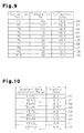
- Fig. 9 shows some of the control data segments D0 to Dn stored in the memory device 25 of Fig. 7.
- the correction data segments D0 to D9 shown in Fig. 9 are stored at predetermined addresses in the memory device 25.
- the correction data segments D0 to D9 are used for digital correction at correction points P1 to P10, which are set at 10°C intervals with respect to the characteristic curve X1 shown in Fig. 8.
- the characteristic curve X1 shows the output signal Vout of the amplification circuit unit 22 when the output of the sensor 1 is not corrected.
- the amplification circuit unit 22 corrects the output of the sensor with the correction data segments D0 to D9 in correspondence with the correction points P1 to P10.
- the characteristic curve X1 is converged to the target value (zero in Fig. 8) regardless of the temperature.
- the amplification circuit unit 22 uses the correction data segment D0 corresponding to the correction point P1 to adjust the resistances of the resistors R1a, R1b, and R2 and the voltage adjustment circuit 9. As a result, +4 is added to the value for the characteristic curve X1 at correction point P1.
- the control circuit 24 is connected to a gradient calculation circuit 27. Based on the correction data for each correction point, the gradient calculation circuit 27 calculates gradient data for performing analog correction on the output of the sensor 1 between correction points and provides the gradient data to the data latch unit 26. Based on the gradient data stored in the data latch unit 26, the amplification circuit unit 22 adjusts the resistances of the resistors R3 and R4 and the voltage adjustment circuit 17 between the correction points.
- Fig. 10 shows gradient data segments S0 to S8 calculated from the correction data segments D0 to D9 shown in Fig. 9.
- the gradient data segments S0 to S8 are calculated from the difference between the correction data segments D0 to D9.
- the resistances of the resistors R3 and R4 and the voltage adjustment circuit 17 are adjusted based on the gradient data segments S0 to S8 at the temperatures between the correction points P1 to P10.
- the switch circuit 16 changes the gradient direction.
- Fig. 8 is a graph schematically showing the output characteristic of the sensor amplification circuit 21 shown in Fig. 6.
- the characteristic curve X1 prior to correction is temperature dependent and has an output level that increases as the temperature rises.
- the characteristic curve X11 shows the output characteristic of the sensor amplification circuit after correction by the amplification circuit unit 22.
- the control circuit 24 reads the correction data corresponding to the temperature from the memory device 25 to adjust the resistances of the resistors R1a, R1b, and R2 and the voltage adjustment circuit 9.
- the digital correction circuit 18 functions to correct the characteristic curve X1 to the target value (the level of zero in Fig. 8) at each of the correction points P1 to P10.
- the characteristic curve X1 is corrected based on the gradient data segments S0 to S8 calculated by the gradient calculation circuit 27 at the temperatures between the correction points P1 to P10.
- the gradient data segment S5 is calculated so as to offset the gradient of the characteristic curve X1 based on the correction data segments D5 and D6.
- the resistances of the resistors R3 and R4 and the voltage adjustment circuit 17 are adjusted based on the gradient data segment S5.
- the gradients shown by the broken lines represent the gradient of the output voltage Va of the analog correction amplifier 15 adjusted based on the gradient data segments S0 to S8.
- the analog correction circuit 19 performs corrections so that the characteristic curve X1 approaches the predetermined target value at temperatures between the correction points P1 to P10.
- the temperature dependency of the characteristic curve X1 is eliminated. That is, the characteristic curve X1 is corrected to the characteristic curve X11, which is flat and generally approximated to the target value.
- the sensor amplification circuit 21 of the first embodiment has the advantages described below.
- the temperature interval between the correction points P1 to P10 is narrowed as the gradient of the characteristic curve X1 becomes steep.
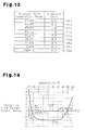
- the memory device 25 stores correction data segments D0a, D1a, D2a, D3a, D4a, D5a, D6a, D7a, D8a, and D9a, which respectively correspond to the correction points P1 to P10.
- Fig. 13 shows gradient data segments S0a, S1a, S2a, S3a, S4a, S5a, S6a, S7a, and S8a for between the correction points P1 to P10 from the correction data of Fig. 12.
- the digital correction circuit18 corrects the characteristic curve X1 to the predetermined target value at the correction points P1 to P10.
- the analog correction circuit 19 corrects the characteristic curve X1 based on the gradient data (Fig. 12) calculated by the gradient calculation circuit 27 at temperatures between the correction points P1 to P10.
- the analog correction is further optimized from the first embodiment. More specifically, the temperature intervals between the correction points P1 to P10 are changed in accordance with the gradient of the characteristic curve X1. This improves the accuracy of the gradient data (Fig. 12). Accordingly, the characteristic curve X1 between the correction points P1 to P10 is corrected to further become closer to the predetermined target value.
- the characteristic curve X1a has a large gradient in a low temperature region (-30°C through 60°C) and a high temperature region (30°C through 60°C).
- the temperature interval is narrowed between the correction points P1 to P6 in the low temperature region.
- the temperature interval is also narrowed between the correction points P7 to P10 in the high temperature region.
- the memory device 25 stores the correction data (not shown) corresponding to the correction points P1 to P10.
- the characteristic curve X1a is corrected to the predetermined target value by the digital correction circuit 18.
- the characteristic curve X1a is corrected by the analog correction circuit 10 based on the inclination data (not shown) calculated by the gradient calculation circuit 27.
- the analog correction is optimized in the third embodiment. That is, the temperature intervals between the correction points P1 to P10 are changed in accordance with the gradient of the characteristic curve X1a shown in Fig. 14. This improves the accuracy of the gradient data. Accordingly, the characteristic curve X12 after correction is even flatter.
- the control circuit 24 determines whether or not correction with the correction data must be performed based on the correction data read from the memory device 25 at each correction point. That is, based on the correction data, the control circuit 24 determines whether or not resistance adjustment must be performed by the digital correction circuit 18 and the analog correction circuit 19 based on the correction data. Resistance adjustment is not performed when it is not necessary.
- control circuit 24 of the fourth embodiment includes a determination unit 28 for determining whether or not resistance adjustment is necessary in the digital correction circuit 18 and the analog correction circuit 19.
- the memory device 25 stores correction data segments D0 to D9 (Fig. 9) respectively corresponding to the correction points P1 to P10 of the characteristic curve X1 (Fig. 8).
- the correction data segment D0 is read from the memory device 25 and the resistance of the digital correction circuit 18 is adjusted based on the correction data segment D0.
- the characteristic curve X1 at the correction point P1 is corrected to the target value.
- the resistance of the analog correction circuit 19 is adjusted based on the gradient data S0 calculated from the correction data segments D0 and D1 for the correction points P1 and P2.
- the characteristic curve X1 is corrected to the target value between the correction points P1 and P2.
- the correction data segment D1 is identical to the correction data segment D0 for the correction point P1.
- the determination unit 28 determines that the resistance of the digital correction circuit 18 at the correction point P2 is not necessary. Accordingly, the resistance adjustment of the digital correction circuit 18 is not performed. Thus, the resistance of the analog correction circuit 19 between the correction points P2 and P3 is not adjusted.
- the correction data segment D2 for correction point P3 is identical to the correction data segment D1 of the correction point P2.
- the resistance of the digital correction circuit 18 is not adjusted.
- the correction data segments D2 and D3 for the correction points P3 and P4 are identical.
- the resistance of the analog correction circuit 19 is not adjusted.
- the correction data segment D3 is identical to the correction data segment D2 for the correction point P3.
- the resistance of the digital correction circuit 18 is not adjusted.
- the gradient data segment S3 differs from the gradient data segment S2 between the correction points P3 and P4.
- the resistance of the analog correction circuit 19 is adjusted based on the gradient data segment S3.
- the correction data segment D4 differs from the correction data segment D3 for the correction point P4.
- the resistance of the digital correction circuit 18 is adjusted.
- the gradient data segment S4 is identical to the gradient data segment S3 between the correction points P4 and P5 for the temperatures between the correction points P5 and P6.
- the resistance of the analog correction circuit 19 is not adjusted.
- the determination unit 28 determines whether or not resistance adjustment of the digital correction circuit 18 or the analog correction circuit 19 is necessary based on the correction data for the correction points P1 to P10.
- the fourth embodiment has the advantages described below.
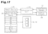
- a fifth embodiment of the present invention will now be discussed with reference to Fig. 17.
- the necessity for resistance adjustment at the correction points P1 to P10 that is, the temperature for reading correction data from the memory device 25 is determined beforehand.
- a determination unit 29 reads all of the correction data stored in the memory device 25 and determines beforehand the temperature of the correction point requiring resistance adjustment (temperature for changing correction data) of the digital correction circuit 18 or the analog correction circuit 19.
- the determination unit 29 stores the determination result in a determination result storage region 30 of the memory device 25.
- the determination unit 29 determines whether resistance adjustment is necessary for the digital correction circuit 18 or the analog correction circuit 19 at correction points P1 to P10. As a result, the control circuit 24 reads the correction data from the memory device 25 only when detecting temperatures corresponding to the one of the correction points P1 to P10 requiring resistance adjustment.
- the number of times correction data is read from the memory device 25 is reduced. This suppresses power supply noise and reduces power consumption.
- a control signal corresponding to the determination result of the determination unit 28 in the fourth embodiment or the determination unit 29 in the fifth embodiment may be provided from outside the amplification circuit 21.
- the determination unit 29 may incorporate the control circuit 24.
Landscapes
- Physics & Mathematics (AREA)
- General Physics & Mathematics (AREA)
- Engineering & Computer Science (AREA)
- Technology Law (AREA)
- Amplifiers (AREA)
- Indication And Recording Devices For Special Purposes And Tariff Metering Devices (AREA)
Applications Claiming Priority (1)
| Application Number | Priority Date | Filing Date | Title |
|---|---|---|---|
| JP2006072659A JP2007248288A (ja) | 2006-03-16 | 2006-03-16 | 温度特性補正方法及びセンサ用増幅回路 |
Publications (2)
| Publication Number | Publication Date |
|---|---|
| EP1835261A2 true EP1835261A2 (de) | 2007-09-19 |
| EP1835261A3 EP1835261A3 (de) | 2017-08-30 |
Family
ID=38180159
Family Applications (1)
| Application Number | Title | Priority Date | Filing Date |
|---|---|---|---|
| EP06124192.3A Withdrawn EP1835261A3 (de) | 2006-03-16 | 2006-11-16 | Verfahren und Schaltung zur Korrektur von temperaturabhängigen Sensoreigenschaften |
Country Status (3)
| Country | Link |
|---|---|
| US (1) | US7857505B2 (de) |
| EP (1) | EP1835261A3 (de) |
| JP (1) | JP2007248288A (de) |
Families Citing this family (9)
| Publication number | Priority date | Publication date | Assignee | Title |
|---|---|---|---|---|
| JP5224361B2 (ja) * | 2008-11-12 | 2013-07-03 | 古河電気工業株式会社 | 光学モジュールとその制御方法 |
| FR2989777B1 (fr) * | 2012-04-23 | 2014-10-24 | Snecma | Correction d'une mesure de temperature d'une sonde de temperature de type a resistance thermometrique |
| CN103852183B (zh) * | 2012-12-07 | 2016-06-29 | 中国核动力研究设计院 | 一种提高热电阻温度计测量精度的方法 |
| JP6579378B2 (ja) * | 2015-12-07 | 2019-09-25 | 三菱マテリアル株式会社 | 異常温度検出回路 |
| CN108781061B (zh) | 2016-03-11 | 2022-04-08 | 株式会社索思未来 | 放大电路、接收电路以及半导体集成电路 |
| US10761041B2 (en) * | 2017-11-21 | 2020-09-01 | Watlow Electric Manufacturing Company | Multi-parallel sensor array system |
| DE102018203465A1 (de) * | 2018-03-08 | 2019-09-12 | Robert Bosch Gmbh | Radarsensorsystem und Verfahren zum Betreiben eines Radarsensorsystems |
| CN108196491B (zh) * | 2018-04-08 | 2023-12-29 | 暨南大学 | 一种有轨电车车内环境实时监测系统及其工作方法 |
| WO2020263175A1 (en) | 2019-06-25 | 2020-12-30 | Choon How Lau | Circuit arrangement and method of forming the same |
Family Cites Families (15)
| Publication number | Priority date | Publication date | Assignee | Title |
|---|---|---|---|---|
| JP3046129B2 (ja) * | 1992-01-24 | 2000-05-29 | 三菱電機株式会社 | 計測装置 |
| JP3953592B2 (ja) | 1997-08-20 | 2007-08-08 | 大和製衡株式会社 | ロードセルのスパン温度補償装置 |
| JP3419274B2 (ja) * | 1997-10-03 | 2003-06-23 | 富士電機株式会社 | センサ出力補償回路 |
| JPH11194061A (ja) | 1998-01-07 | 1999-07-21 | Yazaki Corp | 圧力センサ駆動回路 |
| JP2000214030A (ja) * | 1999-01-26 | 2000-08-04 | Matsushita Electric Works Ltd | 圧力センサ回路 |
| JP3559739B2 (ja) | 1999-11-15 | 2004-09-02 | トヨタ自動車株式会社 | 入力選択出力回路および温度特性補償回路 |
| JP3626066B2 (ja) * | 2000-03-29 | 2005-03-02 | 株式会社 沖マイクロデザイン | 計算装置及び計算方法 |
| JP2002148131A (ja) * | 2000-11-10 | 2002-05-22 | Denso Corp | 物理量検出装置 |
| JP2003084728A (ja) | 2001-09-17 | 2003-03-19 | Citizen Watch Co Ltd | 液晶表示装置の電極駆動電圧発生回路 |
| JP4295472B2 (ja) * | 2002-05-21 | 2009-07-15 | 大成建設株式会社 | 計測値の補正装置及び補正方法 |
| US6879929B2 (en) * | 2002-10-31 | 2005-04-12 | Sun Microsystems | Sense amplifier thermal correction scheme |
| JP3956877B2 (ja) * | 2003-03-18 | 2007-08-08 | 株式会社デンソー | センサ用温度補正装置およびセンサの温度補正方法 |
| JP2007263709A (ja) * | 2006-03-28 | 2007-10-11 | Fujitsu Ltd | 温度特性補正方法及びセンサ用増幅回路 |
| JP5411415B2 (ja) * | 2006-09-25 | 2014-02-12 | スパンション エルエルシー | 温度特性補正回路 |
| RU2009138708A (ru) * | 2007-03-22 | 2011-04-27 | Бейкер Хьюз Инкорпорейтед (Us) | Позиционно-чувствительная калибровка измерений распределенным сенсором температуры |
-
2006
- 2006-03-16 JP JP2006072659A patent/JP2007248288A/ja active Pending
- 2006-11-14 US US11/598,571 patent/US7857505B2/en active Active
- 2006-11-16 EP EP06124192.3A patent/EP1835261A3/de not_active Withdrawn
Also Published As
| Publication number | Publication date |
|---|---|
| US20070214884A1 (en) | 2007-09-20 |
| EP1835261A3 (de) | 2017-08-30 |
| US7857505B2 (en) | 2010-12-28 |
| JP2007248288A (ja) | 2007-09-27 |
Similar Documents
| Publication | Publication Date | Title |
|---|---|---|
| CN1253285A (zh) | 使用热电堆传感器的温度感测电路 | |
| US7149609B2 (en) | Vehicular electronic control unit | |
| EP1835261A2 (de) | Verfahren und Schaltung zur Korrektur von temperaturabhängigen Sensoreigenschaften | |
| CN111596236A (zh) | 具有灵敏度校正和偏移校正功能的磁场传感器及实现方法 | |
| US7625118B2 (en) | Circuit for correcting sensor temperature characteristics | |
| US8421477B2 (en) | Resistance variation detection circuit, semiconductor device and resistance variation detection method | |
| EP1840526A2 (de) | Korrekturverfahren für Temperatureigenschaften und Sensorverstärkungsschaltung | |
| US12436207B2 (en) | Sensor output compensation circuit | |
| JP4255632B2 (ja) | 電気負荷の断線検出装置 | |
| CN115079758B (zh) | 电流输出模块 | |
| JP4249081B2 (ja) | 測定装置及び測定装置の温度補償方法 | |
| JP4642364B2 (ja) | 温度検出回路、温度検出装置、及び光電変換装置 | |
| JP2014178290A (ja) | 電流検出装置、電流検出方法およびプログラム | |
| JP2009145195A (ja) | 温度検出回路 | |
| JPH08278110A (ja) | 光学式センサ | |
| US20230408604A1 (en) | Sensor output compensation circuit | |
| US7345536B2 (en) | Amplifier circuit and control method thereof | |
| US20090027018A1 (en) | Integrated circuit and a method for selecting a voltage in an integrated circuit | |
| CN121656355A (zh) | 气体传感器 | |
| JPH06213435A (ja) | 燃焼機器用制御装置 | |
| JP4508001B2 (ja) | 温度補正回路 | |
| JP4244895B2 (ja) | 物理量センサおよびその製造方法 | |
| JPH1096675A (ja) | 温度補償回路及び温度補償方法 | |
| JP2006013715A (ja) | ゲインコントロール回路 | |
| JP2006170780A (ja) | センサ出力値検出装置 |
Legal Events
| Date | Code | Title | Description |
|---|---|---|---|
| PUAI | Public reference made under article 153(3) epc to a published international application that has entered the european phase |
Free format text: ORIGINAL CODE: 0009012 |
|
| AK | Designated contracting states |
Kind code of ref document: A2 Designated state(s): AT BE BG CH CY CZ DE DK EE ES FI FR GB GR HU IE IS IT LI LT LU LV MC NL PL PT RO SE SI SK TR |
|
| AX | Request for extension of the european patent |
Extension state: AL BA HR MK YU |
|
| RAP1 | Party data changed (applicant data changed or rights of an application transferred) |
Owner name: FUJITSU MICROELECTRONICS LIMITED |
|
| RAP1 | Party data changed (applicant data changed or rights of an application transferred) |
Owner name: FUJITSU SEMICONDUCTOR LIMITED |
|
| RAP1 | Party data changed (applicant data changed or rights of an application transferred) |
Owner name: SPANSION LLC |
|
| RAP1 | Party data changed (applicant data changed or rights of an application transferred) |
Owner name: CYPRESS SEMICONDUCTOR CORPORATION |
|
| PUAL | Search report despatched |
Free format text: ORIGINAL CODE: 0009013 |
|
| AK | Designated contracting states |
Kind code of ref document: A3 Designated state(s): AT BE BG CH CY CZ DE DK EE ES FI FR GB GR HU IE IS IT LI LT LU LV MC NL PL PT RO SE SI SK TR |
|
| AX | Request for extension of the european patent |
Extension state: AL BA HR MK RS |
|
| RIC1 | Information provided on ipc code assigned before grant |
Ipc: G01D 3/036 20060101ALI20170727BHEP Ipc: G01D 3/02 20060101AFI20170727BHEP |
|
| RIN1 | Information on inventor provided before grant (corrected) |
Inventor name: OKAJIMA, TAKUYA Inventor name: WATAI, TAKAHIRO Inventor name: AOKI, KOJU Inventor name: SAKIMA, HIROYUKI Inventor name: MIZUTANI, MASAYA |
|
| STAA | Information on the status of an ep patent application or granted ep patent |
Free format text: STATUS: THE APPLICATION HAS BEEN PUBLISHED |
|
| AKY | No designation fees paid | ||
| AXX | Extension fees paid |
Extension state: AL Extension state: HR Extension state: RS Extension state: BA Extension state: MK |
|
| REG | Reference to a national code |
Ref country code: DE Ref legal event code: R108 |
|
| STAA | Information on the status of an ep patent application or granted ep patent |
Free format text: STATUS: THE APPLICATION IS DEEMED TO BE WITHDRAWN |
|
| 18D | Application deemed to be withdrawn |
Effective date: 20180301 |