EP1832910B1 - Lichtwellenleiterbeleuchtungsvorrichtung und Überprüfungsvorrichtung für Hologramme - Google Patents
Lichtwellenleiterbeleuchtungsvorrichtung und Überprüfungsvorrichtung für Hologramme Download PDFInfo
- Publication number
- EP1832910B1 EP1832910B1 EP07004668A EP07004668A EP1832910B1 EP 1832910 B1 EP1832910 B1 EP 1832910B1 EP 07004668 A EP07004668 A EP 07004668A EP 07004668 A EP07004668 A EP 07004668A EP 1832910 B1 EP1832910 B1 EP 1832910B1
- Authority
- EP
- European Patent Office
- Prior art keywords
- light
- hologram
- medium
- inspection apparatus
- diffraction
- Prior art date
- Legal status (The legal status is an assumption and is not a legal conclusion. Google has not performed a legal analysis and makes no representation as to the accuracy of the status listed.)
- Active
Links
Images






Classifications
-
- G—PHYSICS
- G07—CHECKING-DEVICES
- G07D—HANDLING OF COINS OR VALUABLE PAPERS, e.g. TESTING, SORTING BY DENOMINATIONS, COUNTING, DISPENSING, CHANGING OR DEPOSITING
- G07D7/00—Testing specially adapted to determine the identity or genuineness of valuable papers or for segregating those which are unacceptable, e.g. banknotes that are alien to a currency
- G07D7/06—Testing specially adapted to determine the identity or genuineness of valuable papers or for segregating those which are unacceptable, e.g. banknotes that are alien to a currency using wave or particle radiation
- G07D7/12—Visible light, infrared or ultraviolet radiation
- G07D7/121—Apparatus characterised by sensor details
-
- G—PHYSICS
- G03—PHOTOGRAPHY; CINEMATOGRAPHY; ANALOGOUS TECHNIQUES USING WAVES OTHER THAN OPTICAL WAVES; ELECTROGRAPHY; HOLOGRAPHY
- G03H—HOLOGRAPHIC PROCESSES OR APPARATUS
- G03H1/00—Holographic processes or apparatus using light, infrared or ultraviolet waves for obtaining holograms or for obtaining an image from them; Details peculiar thereto
- G03H1/02—Details of features involved during the holographic process; Replication of holograms without interference recording
-
- G—PHYSICS
- G01—MEASURING; TESTING
- G01B—MEASURING LENGTH, THICKNESS OR SIMILAR LINEAR DIMENSIONS; MEASURING ANGLES; MEASURING AREAS; MEASURING IRREGULARITIES OF SURFACES OR CONTOURS
- G01B11/00—Measuring arrangements characterised by the use of optical techniques
- G01B11/30—Measuring arrangements characterised by the use of optical techniques for measuring roughness or irregularity of surfaces
-
- G—PHYSICS
- G01—MEASURING; TESTING
- G01N—INVESTIGATING OR ANALYSING MATERIALS BY DETERMINING THEIR CHEMICAL OR PHYSICAL PROPERTIES
- G01N21/00—Investigating or analysing materials by the use of optical means, i.e. using sub-millimetre waves, infrared, visible or ultraviolet light
- G01N21/84—Systems specially adapted for particular applications
- G01N21/88—Investigating the presence of flaws or contamination
- G01N21/89—Investigating the presence of flaws or contamination in moving material, e.g. running paper or textiles
- G01N21/892—Investigating the presence of flaws or contamination in moving material, e.g. running paper or textiles characterised by the flaw, defect or object feature examined
-
- G—PHYSICS
- G02—OPTICS
- G02B—OPTICAL ELEMENTS, SYSTEMS OR APPARATUS
- G02B6/00—Light guides; Structural details of arrangements comprising light guides and other optical elements, e.g. couplings
-
- G—PHYSICS
- G03—PHOTOGRAPHY; CINEMATOGRAPHY; ANALOGOUS TECHNIQUES USING WAVES OTHER THAN OPTICAL WAVES; ELECTROGRAPHY; HOLOGRAPHY
- G03H—HOLOGRAPHIC PROCESSES OR APPARATUS
- G03H1/00—Holographic processes or apparatus using light, infrared or ultraviolet waves for obtaining holograms or for obtaining an image from them; Details peculiar thereto
- G03H1/22—Processes or apparatus for obtaining an optical image from holograms
- G03H1/2286—Particular reconstruction light ; Beam properties
-
- G—PHYSICS
- G07—CHECKING-DEVICES
- G07D—HANDLING OF COINS OR VALUABLE PAPERS, e.g. TESTING, SORTING BY DENOMINATIONS, COUNTING, DISPENSING, CHANGING OR DEPOSITING
- G07D7/00—Testing specially adapted to determine the identity or genuineness of valuable papers or for segregating those which are unacceptable, e.g. banknotes that are alien to a currency
- G07D7/003—Testing specially adapted to determine the identity or genuineness of valuable papers or for segregating those which are unacceptable, e.g. banknotes that are alien to a currency using security elements
- G07D7/0032—Testing specially adapted to determine the identity or genuineness of valuable papers or for segregating those which are unacceptable, e.g. banknotes that are alien to a currency using security elements using holograms
-
- G—PHYSICS
- G03—PHOTOGRAPHY; CINEMATOGRAPHY; ANALOGOUS TECHNIQUES USING WAVES OTHER THAN OPTICAL WAVES; ELECTROGRAPHY; HOLOGRAPHY
- G03H—HOLOGRAPHIC PROCESSES OR APPARATUS
- G03H1/00—Holographic processes or apparatus using light, infrared or ultraviolet waves for obtaining holograms or for obtaining an image from them; Details peculiar thereto
- G03H1/0005—Adaptation of holography to specific applications
- G03H1/0011—Adaptation of holography to specific applications for security or authentication
-
- G—PHYSICS
- G03—PHOTOGRAPHY; CINEMATOGRAPHY; ANALOGOUS TECHNIQUES USING WAVES OTHER THAN OPTICAL WAVES; ELECTROGRAPHY; HOLOGRAPHY
- G03H—HOLOGRAPHIC PROCESSES OR APPARATUS
- G03H1/00—Holographic processes or apparatus using light, infrared or ultraviolet waves for obtaining holograms or for obtaining an image from them; Details peculiar thereto
- G03H1/22—Processes or apparatus for obtaining an optical image from holograms
- G03H1/2202—Reconstruction geometries or arrangements
- G03H2001/2223—Particular relationship between light source, hologram and observer
- G03H2001/2231—Reflection reconstruction
-
- G—PHYSICS
- G03—PHOTOGRAPHY; CINEMATOGRAPHY; ANALOGOUS TECHNIQUES USING WAVES OTHER THAN OPTICAL WAVES; ELECTROGRAPHY; HOLOGRAPHY
- G03H—HOLOGRAPHIC PROCESSES OR APPARATUS
- G03H1/00—Holographic processes or apparatus using light, infrared or ultraviolet waves for obtaining holograms or for obtaining an image from them; Details peculiar thereto
- G03H1/22—Processes or apparatus for obtaining an optical image from holograms
- G03H1/2202—Reconstruction geometries or arrangements
- G03H2001/2244—Means for detecting or recording the holobject
- G03H2001/2247—Means for detecting or recording the holobject for testing the hologram or holobject
-
- G—PHYSICS
- G03—PHOTOGRAPHY; CINEMATOGRAPHY; ANALOGOUS TECHNIQUES USING WAVES OTHER THAN OPTICAL WAVES; ELECTROGRAPHY; HOLOGRAPHY
- G03H—HOLOGRAPHIC PROCESSES OR APPARATUS
- G03H2222/00—Light sources or light beam properties
- G03H2222/34—Multiple light sources
Definitions
- the present invention relates to an optical fiber illumination device which irradiates illumination light onto a medium to be inspected, such as a card, and an inspection apparatus which inspects a medium to be inspected, such as a hologram-attached paper instrument.
- a diffraction optical variable device (to be referred to as optical OVD), a typical example of which is a hologram, is a device processed to induce the light diffraction phenomenon on the surface thereof, and it has a pattern which generates vivid colors due to optical diffraction and interference caused by the diffraction pattern.
- the hologram has optical characteristics different from those of the ordinary printing and therefore it is used as a security thread for paper instruments of, for example, coupons and securities as well as cards such as credit cards.
- the hologram is realized as means for determining the authenticity of these media.
- EP 1 195 712 A1 describes a card authenticity judging apparatus.
- Jpn. Pat. Appln. KOKAI Publications No. 2004-150885 , No. 2002-221494 and No. 2002-221496 disclose an inspection apparatus which irradiates a laser beam on a surface of a medium to be inspected and inspects the reflection diffraction image with a light receiving sensor, an apparatus which inspects a moving medium to be inspected with a line illumination, etc.
- Jpn. Pat. Appln. KOKAI Publication No. 2001-307173 discloses an inspection apparatus which identifies the authenticity of a hologram, using a spotlight system which projects measurement light, and a plurality of light-receiving systems respectively detecting a plurality of reflection diffraction light components reflection-diffracted by the diffraction pattern of the hologram.
- Jpn. Pat. Appln. KOKAI Publications No. 2002-221494 discloses an illumination device which illuminates a hologram, in which a plurality of Selfoc (trademark) lenses are arranged at predetermined angles to irradiate light onto the hologram.
- an illumination device which uses optical fibers that is less expensive as compared to Selfoc lenses, includes an optical fiber light guide, in which the elemental fibers of the optical fibers are arranged to be vertical to the light-emitting surface of the optical fiber light guide.
- One end of the optical fiber light guide is located on the light source side, and the light emitted from the light source is transmitted through the optical fiber and emitted from the other end of the optical fiber light guide.
- the conventional inspection apparatus of the type which utilizes laser light entails such drawbacks as that the conditions for stopping the medium to be inspected for observation are severe, and it requires much time to collect information and for identification process.
- the conventional inspection apparatus designed to inspect a moving medium entails such a drawback that the rattling of the medium to be inspected causes an adverse effect to the results of the inspection.
- the light-emitting surface of the optical fiber light guide is set to be inclined at a specific angle with respect to the hologram.
- the light is strong and concentrated in a section close to the light-emitting surface of the optical fiber light guide, whereas the light is weak and diffused in a section far from the light-emitting surface.
- a hologram inspection apparatus that uses such an illumination is not able to stably obtain the data within the entire view field to be inspected, which causes an adverse effect on the inspection accuracy.
- the present invention has been contrived in consideration of the above-described circumstances, and its object is to provide an optical fiber illumination apparatus which can illuminate a region to be inspected with stably spreading light and at a stable intensity, as well as an inspection apparatus which can stably detect the authenticity and damage of a hologram-attached medium to be inspected.
- an inspection apparatus according to claim 1.
- a paper instrument inspection apparatus includes a holder mechanism 14 which holds a paper instrument 12 such as a valuable paper certificate to which a hologram 10 to be inspected is attached, a light source unit 16 which irradiates illumination light for inspection on the paper instrument, a first light receiving sensor 18 which receives reflection light from the hologram 10 and a second light receiving sensor 20 which receives transmitted light passed through the paper instrument.
- a paper instrument 12 such as a valuable paper certificate to which a hologram 10 to be inspected is attached
- a light source unit 16 which irradiates illumination light for inspection on the paper instrument
- a first light receiving sensor 18 which receives reflection light from the hologram 10
- a second light receiving sensor 20 which receives transmitted light passed through the paper instrument.
- the hologram 10 includes, for example, a round-shaped metal foil 10a attached onto the paper instrument 12 and a diffraction pattern (diffraction grating) 10b of a desired shape, for example, in this embodiment a shape of letter "A" formed on the metal foil.
- the hologram 10 when visible light is irradiated thereon at a predetermined angle, reflects diffraction light corresponding to the diffraction pattern 10b, and shows a rainbow-color characteristic pattern.
- the holder mechanism 14 is formed of, for example, a plurality of rollers 22 and belts, which are not shown in the figure, and it holds the paper instrument 12 in a state where a tension is applied thereto, that is, in a tense state without looseness.
- the light source unit 16 includes a spotlight unit which irradiate spotlight illumination onto an illumination area 34 that is larger than the area of the hologram 10 to include it within the region.
- the spotlight unit is, for example, an incandescent light source, and it irradiates illumination light of a wide range of wavelengths including those from the visible light to the near infrared region.
- the light source unit 16 is set at a predetermined angle with respect to the paper instrument 12 and it irradiates onto the hologram illumination light having an optimized directivity to be able to obtain a diffraction image by the diffraction pattern 10b of the object hologram 10.
- the first light receiving sensor 18, which serves as the first light-receiving unit, is provided on the same surface side as the light source unit 16 with respect to the paper instrument 12, at a position to receive the diffraction light from the hologram 10.
- the first light receiving sensor 18 has an image forming lens 19, and receives the reflection light image formed by the image-forming lens.
- a point photosensor, a monochrome CCD sensor, a color CCD sensor, etc. can be employed as the first light receiving sensor 18, a point photosensor, a monochrome CCD sensor, a color CCD sensor, etc., can be employed.
- the second light receiving sensor 20 which serves as the second light-receiving unit, is provided on an opposite surface side to the light source unit 16 with respect to the paper instrument 12, at a position to receive the transmitted light passing through the paper instrument 12 around the hologram 10.
- the second light receiving sensor 20 has an image forming lens 21, and receives the image of the transmitted light formed by the image forming lens.
- a point photosensor, a monochrome CCD sensor, a color CCD sensor, etc. can be employed as the second light receiving sensor 20, a point photosensor, a monochrome CCD sensor, a color CCD sensor, etc., can be employed.
- the paper instrument inspection apparatus includes a first identification processing unit 28, a second identification processing unit 30, a light source driver 32 which drives the light source unit 16 and a control unit 36 which controls the operation of the entire device.
- the first identification processing unit 28 processes data detected by the first light receiving sensor 18 to extract the characteristics and compares the extracted characteristics with reference data stored in an identification reference memory 26, thereby determining the authenticity of the hologram 10.
- the second identification processing unit 30 processes data detected by the second light receiving sensor 20 to extract the characteristics and compares the extracted characteristics with reference data stored in the identification reference memory 26, thereby identifying the damage or deficiency of the hologram 10 and paper instrument 12.
- the first and second identification processing units 28 and 30 serve as identification processing units.
- the conditions for which the diffraction light appears from the hologram 10 to be inspected depend on the orientation and pitch of the diffraction grating of the hologram.
- the light irradiated from the light source unit 16 is applied to the hologram at an incident angle ⁇ 1, which is optimized with a direction B orthogonal to the diffraction grating 10b of the hologram 10.
- regular reflection light appears from the diffraction grating 10b at an angle ⁇ 1. Diffraction light is observed in a region between the incident angle and the regular reflection angle.
- the incident angle of the illumination light to the hologram 10 varies depending on the location on the hologram as shown in FIG. 5 ; the wavelengths of the diffraction light components ⁇ 2, ⁇ 3 and ⁇ 4 are shifted from each other.
- a color CCD sensor is employed as the first light receiving sensor 18, an image received with the first light-sensitive sensor is obtained as a rainbow-color image in which the wavelength varies depending on the location.
- the first identification processing unit 28 processes data detected by the first light receiving sensor 18 to extract the characteristics as a two-dimensional image and compares the extracted image with the reference data stored in an identification reference memory 26, thereby determining the authenticity of the hologram 10.
- the second identification processing unit 30 processes data detected by the second light receiving sensor 20 to extract the characteristics as a one-dimensional or two-dimensional image and compares the extracted image with reference data stored in the identification reference memory 26. In this manner, the second identification processing unit 30 identifies the damage or deficiency of the hologram 10.
- the paper instrument inspection apparatus can inspect the authenticity of the hologram by irradiating illumination spotlight optimized for the hologram 10 attached to a paper instrument 12, and detecting the diffraction light data from the hologram.
- those instruments with similar holograms are attached for the purpose of making counterfeits and counterfeit hologram media are not able to reproduce intrinsic characteristics such as diffraction grating patterns or pitches which completely match those of the genuine instruments, and therefore the above-described diffraction light cannot be observed from these counterfeits.
- the authenticity of a hologram can be effectively determined.
- the chipping and damaged state of the metal foil used for the hologram can be inspected by detecting the data of the transmitted light having passed through the paper instrument.
- a rainbow-color striped pattern can be observed when white light is applied onto the surface thereof.
- the principle of the mechanism here is that light reflecting on the metal foil reproduces the image, and therefore the hologram in its basic principle has a property in which light is hardly transmitted. Therefore, utilizing the property, the damage or chipping of the metal foil can be inspected with the same inspection apparatus by detecting the data of the transmitted light having passed through the hologram.
- the spotlight illumination When the spotlight illumination is used as inspection light to be irradiated from the light source unit, it is possible to realize the illumination optimized for the characteristics of the diffraction grating of the hologram. If diffused illumination or large-area illumination is employed, there are light components having directivities other than that of the optical illumination. This increases the risk in which these light components may match some other diffraction grating and also similar rainbow-color characteristics can be obtained. From this point of view, it is desirable that the illumination light necessary for the specification should be the minimum possible light optimized for the object to be inspected. The spotlight illumination device meets this requirement.
- the second light receiving sensor which detects the transmitting light having passed through the paper instrument
- a photodiode or the like which is a sensor which can detect one-dimensional data
- an image sensor such as a CCD sensor which can obtain two-dimensional image data
- the image sensor is preferable.
- color image sensors such as color CCD sensors can be used. With use of such color image sensors, the performance of the identification can be further improved.
- a white illumination light or a spotlight having such a wide wavelength range characteristics as those of an incandescent light source should preferably be employed.
- the rainbow color characteristics of the rainbow hologram to be inspected can be exploited to the maximum.
- the hologram has an inclined surface or slightly irregular surface with projections and recesses, the rainbow color characteristics can be stably obtained. How the rainbow color characteristics show vary depending on the conditions, and therefore a stable performance can be achieved by identifying the object based on evaluation criteria such as the presence/absence, frequency, etc. of the characteristics.
- the transmitted light should be designated to light of the near-infrared wavelength region.
- the influence caused by the pattern of the background printing in the periphery of the hologram can be reduced, and therefore the performance of inspecting the damage and chipping can be enhanced, which makes it even more effective.
- the inspection apparatus includes a conveying mechanism 15 which conveys the paper instrument 12 along a direction C which is in parallel with the paper surface while applying a tension to the paper instrument along the plane direction of the paper instrument.
- the conveying mechanism 15 includes a plurality of conveying rollers 40 which convey the paper instrument while holding it between the respective rollers and a conveying belt which is not shown in the figure.
- illumination light is irradiated from the light source unit 16 onto the illumination area 34 including the hologram 10 while conveying the paper instrument 12 by the conveying mechanism 15.
- the reflection light from the hologram is detected by the first light receiving sensor 18 and the transmitted light having passed the paper instrument is detected by the second light receiving sensor 20.
- the second comparative example is identical to that of the first embodiment already described. Therefore, the same parts are designated by the same reference numerals and the detailed explanations therefor will be omitted here.
- the second comparative example it is possible to obtain an operational effect similar to that of the first embodiment. Further, the second comparative example is able to inspect the paper instrument while conveying it, and therefore it can be applied to more various usages.
- the paper instrument inspection apparatus includes two illumination units as the light source unit 16. More specifically, the light source unit 16 includes a spotlight device 16a and a transmitting illumination light device 16b which irradiates illumination light to transmit the paper instrument.
- the spotlight device 16a irradiates spotlight illumination onto an illumination area 34a in which a hologram 10 is provided.
- the spotlight device 16a is formed as a light source which irradiates illumination light of the visible light range.
- the spotlight device 16a is set at a predetermined angle with respect to the paper instrument 12 and it irradiates onto the hologram illumination light having an optimized directivity to be able to obtain a diffraction image by the diffraction pattern 10b of the object hologram 10.
- the transmitting illumination light device 16b irradiates illumination light to transmit the paper instrument, onto the illumination area 34b larger than the area of the hologram 10 to include it therewithin.
- the transmitting illumination light device 16b is formed as a light source which irradiates illumination light of the near-infrared region.
- the third comparative example it is possible to obtain an operational effect similar to that of the first comparative example. Further, since this example has such a light source which includes an illumination light which irradiates illumination light of a wavelength range which reflects on a hologram and another illumination light which irradiates illumination light of a wavelength range which transmits the paper instrument.
- Each of these illumination light devices can be set to exhibit the optimal performance for each respective detecting operation. More specifically, the spotlight device 16a is formed to have a spot diameter of the same size as that of the hologram 10, and thus the intensity and uniformity of the illumination light can be further enhanced, thereby making it possible to improve the efficiency of the detection.
- the wavelength range of the illumination light of the transmitting illumination light device 16b is made different from that of the spotlight device 16a, and thus the interference between the wavelength ranges can be prevented. Further, when the wavelength range of the illumination light of the transmitting illumination light device 16b is set to the near-infrared region, the influence by the pattern of the background printing on the paper instrument can be reduced. Thus, the light illumination of the device 16b can be made transmissible through the paper instrument reliably.
- the first and second light receiving sensors line sensors can be employed.
- the shape of the spot of the light source device is not limited to circular, but it may be an arbitrary shape.
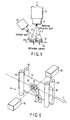
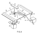
- this hologram inspecting device includes a holder-conveying mechanism 14 which holds, as a medium to be inspected, a paper instrument 12 to which a hologram 10 is attached, and conveys it in a predetermined direction B, an optical fiber illumination device 16 functioning as a light source unit which irradiates inspection illumination light onto a surface, more specifically, a to-be-inspected surface 12a of a paper instrument 12 containing a hologram 10, an image pickup section 18 serving as a first light-receiving sensor which pick ups an image of diffraction light from the hologram and a second light receiving sensor 20 which receives transmitted light having passed the paper instrument.
- an optical fiber illumination device 16 functioning as a light source unit which irradiates inspection illumination light onto a surface, more specifically, a to-be-inspected surface 12a of a paper instrument 12 containing a hologram 10
- an image pickup section 18 serving as a first light-receiving sensor which pick ups an image of diffraction light from the
- the hologram 10 includes, for example, a round-shaped metal foil 10a attached onto the paper instrument 12 and a diffraction pattern (diffraction grating) 10b of a desired shape on the metal foil.
- the hologram 10 when visible light is irradiated thereon at a predetermined angle, reflects diffraction light corresponding to the diffraction pattern 10b, and shows a rainbow-color characteristic pattern.
- the conditions for which the diffraction light appears from the hologram 10 to be inspected depend on the orientation and pitch of the diffraction grating of the hologram.
- the incident light is applied to the hologram 10 at an incident angle (elevation angle) ⁇ 1, which is optimized with a direction B orthogonal to the diffraction grating 10b of the hologram 10 and a rotation angle ⁇ 1 (an angle of the incident light to a direction Y perpendicular to the conveying direction B or to the transfer direction B).
- incident angle ⁇ 1 an angle of the incident light to a direction Y perpendicular to the conveying direction B or to the transfer direction B.
- regular reflection light appears from the diffraction grating 10b at an angle ⁇ 1. Diffraction light is observed in a region between the incident angle and the regular reflection angle.
- FIG. 12A which is a diagram viewed from an arrow direction a in FIG. 11
- an incident light is applied to the hologram 10 at an angle ⁇ 1 which is obtained by synthesizing an elevation angle ⁇ 1 and a rotation angle ⁇ 1
- regular reflection light appears from the diffraction grating 10b at an angle ⁇ 1 and diffraction light is observed in a region between the incident angle and the regular reflection angle.
- FIG. 12B which is a diagram viewed from an arrow direction b in FIG.
- the holder-conveying mechanism 14 is formed of, for example, a plurality of rollers 22 and a belt, which is not shown in the figure, and it holds the paper instrument 12 in a state where a tension is applied thereto, that is, in a tense state without looseness, and conveys the instrument in the predetermined direction B relatively with respect to the optical fiber illumination device 16 and the image pickup device 18.
- the optical fiber illumination device 16 includes a light source 124, an optical fiber 126 formed of a bundle of a plurality of elemental fibers 126a, and a light guide 128 serving as a guide member which holds the light emitting end portion of the optical fiber.
- a light source 124 for example, a fluorescent lamp or a halogen lamp can be employed.
- the proximal end of the optical fiber 16 is optically connected to the light source 124, and the light emitting end portion of the optical fiber is held by the light guide 128.
- the optical fiber 16 guides the light emitted from the light source 124 and emits the light from its emitting end.
- the light guide 128 is made of, for example, aluminum to have a rectangular parallelepiped shape, and has a flat light emitting surface 130.
- the light guide 128 is provided above the paper instrument in such a state that the emitting surface 13 faces the to-be-inspected surface 12a of the paper instrument 12 with the emitting surface 13 being in parallel with the surface 12a.
- the light guide 128 which holds the light emitting end of the optical fiber 126 is provided at a predetermined angle with respect to the paper instrument 12, and it irradiates onto the hologram illumination light having an optimized directivity to be able to obtain a diffraction image by the diffraction pattern 10b of the object hologram 10. That is, the light guide 128 is arranged at a position of an elevation angle ⁇ 1 ( FIG. 13A ) and an elevation angle ⁇ 1 ( FIG. 14 ), where at least one diffraction pattern emits diffraction light to the hologram 10 having the diffraction patterns 10b, attached to the paper instrument 12, and the diffraction light is made incident on the image pickup section 18.
- the elemental fibers 126a which form the optical fiber is buried in the light guide 128, and the light emitting end is located at the light emitting surface 130 of the light guide.
- FIG. 13A which is a diagram viewed from the conveying direction B in FIG. 9
- the elemental fibers 126a are each situated to incline by a predetermined angle ⁇ 1, which is not 90 degrees, with respect to the emitting surface 130.
- the inclining angle ⁇ 1 of each of the elemental fibers 126a coincides with an angle which is obtained by synthesizing the elevation angle ⁇ 1 at which the reflection diffraction light is generated from the hologram 10 to be inspected and the rotation angle ⁇ 1.
- the elemental fibers 126a are arranged in line, for example, in one column in a direction orthogonal to the direction B in which the paper instrument 12 is conveyed.
- FIG. 14 which is a diagram viewed from a direction perpendicular to the conveying direction B in FIG. 9
- the elemental fibers 126a are each situated to incline by a predetermined angle ⁇ 1, which is not 90 degrees, with respect to the emitting surface 130.
- the inclining angle ⁇ 1 of each of the elemental fibers 126a coincides with an angle which is obtained by synthesizing the elevation angle ⁇ 1 and the rotation angle ⁇ 1.
- a plurality of V-letter grooves 131 are formed side by side, and the elemental fibers 126a are respectively engaged in the V-shaped grooves 131 each to be aligned at a position of a predetermined angle.
- the illumination light irradiated from the emitting end of the optical fiber 162 onto the paper instrument 12 has a slender irradiation region E extending in a direction orthogonal to the paper instrument conveying direction B.
- elemental fibers 126a may be arranged not only in one column, but also two or more lines side by side in the light guide 128.
- the image pickup section 18 is provided on the same side of the paper instrument 12 as that of the light guide 128, and it is situated at a position where the reflection diffraction light from the hologram 10 is received.
- a line sensor is employed as the image pickup section 18.
- the image pickup section 18 is arranged in a direction orthogonal to the direction B in which the paper instrument 12 is conveyed, and situated to face the irradiation region E of the optical fiber illumination device 16.
- a monochrome point photosensor, a color point photosensor, a monochrome CCD sensor, a color CCD sensor, etc. can be employed as the image pickup section 18.
- the second light-receiving sensor 20 which functions as the second light receiving section is provided on an opposite side to the light guide 128 with regard to the paper instrument 12, and it is situated at a position where the transmitted light having passed through the paper instrument 12 around the hologram 10 is received.
- the second light-receiving sensor 20 has an image-forming lens 12, and it receives the image of the transmitted light formed with this image-forming lens.
- a point photosensor, a monochrome CCD sensor, a color CCD sensor, etc. can be employed as the second image receiving sensor 20.
- the hologram inspection apparatus includes an image processing unit 125, a first identification processing unit 134, a second identification processing unit 138, a light source driver 136 which drives the light source unit 16 and a control unit 140 which controls the operation of the entire device.
- the image processing unit 28 processes detected data received by the image pickup section 18 to extract the characteristics.
- the first identification processing unit 134 compares the detected image obtained by the image processing section with reference data stored in an identification reference memory 132, thereby determining the authenticity of the hologram 10 as well as the damage and deficiency of the hologram 10.
- the second identification processing unit 138 processes data detected by the second light receiving sensor 20 to extract the characteristics and compares the extracted characteristics with reference data stored in the identification reference memory 132, thereby identifying the damage or deficiency of the hologram 10 and paper instrument 12.
- the first and second identification processing units 134 and 138 serve as identification processing units.
- the paper instrument 12 has the hologram 10 attached thereto and having the diffraction pattern 10b which diffracts and reflects the incident light made at an angle of ⁇ 1 in the vertical direction.
- the paper instrument 12 is conveyed in the conveying direction B by the holder-conveying mechanism 14.
- the light source 124 is turned on so as to apply the illumination light from the emitting end of the optical fiber 126 provided in the light guide 128 towards the hologram 10 on the paper instrument 12.
- the hologram 10 on the paper instrument 12 passes through the irradiation region E, the light is constantly applied thereon from the optical fiber inclined at an angle ⁇ 1 and thus the diffraction reflection light reflects stably from the entire region of the diffraction pattern 10b within the hologram 10 in the vertical direction.
- the incident light is radiated on the hologram 10 at an angle of elevation angle of ⁇ 1 and a rotation angle ⁇ 1
- the diffraction light of the diffraction pattern 10b is made incident on the image pickup section 18 at the maximum intensity.
- the diffraction light from the hologram 10 is received by the image pickup section 18.
- the image pickup section 18 converts the received diffraction light into an electrical signal, which is input to the image processing unit 125.
- the image processing unit 125 processes the detected data input from the image pickup section 18 and extracts the characteristics as a one-dimensional or two-dimensional image.
- the diffraction pattern 10b on the hologram 10 contains a damage such as chipping or peeling-off, not reflection diffraction light is detected from the damaged section.
- the hologram 10 has such a fatigue by which the surface state is degraded, caused by scratch or wrinkle, the diffraction light may not be obtained or it may be weak in intensity.
- the diffraction pattern 10b which is naturally supposed to exist, is not present, or there is a different diffraction pattern, such a phenomenon that there is no diffraction reflection light occurs.
- the first identification processing unit 134 compares the image data transferred from the image processing section 125 with the reference data stored in the identification reference memory 132, and thus identifies the damage and deficiency as well as the authenticity of the hologram 10.
- the light component that hits the hologram 10 is shut off by the metal foil 10a and therefore it is not substantially transmitted through the paper instrument.
- the other light component which hits the area around the hologram 10 transmits the paper instrument 12 and it is received by the second light receiving sensor 20.
- the amount of the light component shut off by the metal foil 10a serving as a non-light transmitting region is extremely small, the data of the metal foil can be obtained from the non-light-transmitting region.
- the second identification processing unit 138 processes data detected by the second light receiving sensor 20 to extract the characteristics as a one-dimensional image or two-dimensional image and compares the extracted characteristics with reference data stored in the identification reference memory 132. In this manner, the second identification processing unit 138 identifies the damage or deficiency of the hologram 10.
- the elemental fibers 126a of the optical fiber 126 are arranged in lines side by side so as to have a predetermined angle ⁇ 1 with respect to the light emitting surface of the light guide 128, and the light guide and medium to be inspected are arranged such that the emitting surface of the light guide is in parallel with the to-be-inspected surface of the medium.
- the distance taken vertically between the light emitting end each elemental wire 126a and the to-be-inspected surface becomes constant for every elemental fiber. Therefore, within the view field of the inspection, that is, the illumination region E, the spreading and intensity of the light irradiated from the optical fiber 126 can be made uniform.
- the entire hologram 10 can be evenly illuminated with the light emitted from the optical fiber 126 containing the component of a particular illumination angle of ⁇ 1.
- similar advantageous effects to those of the first comparative example described above can be obtained.
- stable reflection diffraction light can be obtained from the entire region of the hologram 10.
- the first embodiment described above is described in connection with the device which inspects a hologram having a single type of diffraction pattern, whereas the second embodiment is directed to a hologram inspection apparatus having a structure which can inspect a hologram having two or more types of diffraction patterns.
- the optical fiber 126 of the optical fiber illumination apparatus 16 includes a plurality of elemental fibers arranged to incline at angles ⁇ 1 (an angle obtained by synthesizing ⁇ 1 and ⁇ 1) and ⁇ 2 (an angle obtained by synthesizing ⁇ 2 and ⁇ 2) to respectively correspond to the diffraction patterns 10b and 10c.
- first elemental fibers 126a which form the optical fiber are buried in the light guide 128 in the emitting end of the optical fiber 126, and the light emitting ends thereof are located to meet the emitting surface 130 of the light emitting surface.
- the first elemental fibers 126a are each placed to incline by a predetermined angle ⁇ 1 which does not include 90 degrees with respect to the emitting surface 130.
- each first elemental fiber coincides with an angle which is obtained by synthesizing the rotation angle ⁇ 1 and the particular incident angle (elevation angle) ⁇ 1 at which reflection diffraction light is generated from the diffraction pattern 10b of the hologram 10 to be inspected.
- these elemental fibers 126a are arranged in lines side by side, for example, in one column along a direction orthogonal to the direction B in which the paper instrument 12 is conveyed.
- a plurality of second elemental fibers 126b which form the optical fiber are buried in the light guide 128 in the emitting end of the optical fiber 126, and the light emitting ends thereof are located to meet the emitting surface 130 of the light emitting surface.
- the second elemental fibers 126b are each placed to incline by a predetermined angle ⁇ 2 which does not include 90 degrees with respect to the emitting surface 130.
- the inclining angle ⁇ 2 of each first elemental fiber coincides with an angle which is obtained by synthesizing the rotation angle ⁇ 2 and the particular incident angle (elevation angle) ⁇ 2 at which reflection diffraction light is generated from the diffraction pattern 10b of the hologram 10 to be inspected.
- these elemental fibers 126b are arranged in lines side by side, for example, in one column in a direction orthogonal to the direction B in which the paper instrument 12 is conveyed.
- the second elemental fibers 126b are provided side by side substantially in parallel with the first elemental fibers 126a with an interval therebetween. It should be noted that the proximal end of the optical fiber 126 is connected to the common light source 124.
- the light guide 128 is provided at such a position that the emitting surface 130 faces the to-be-inspected surface 12a of the paper instrument 12 as a medium to be inspected, with these surfaces being arranged in parallel with each other.
- the first elemental fibers 126a and second elemental fibers 126b of the optical fiber are arranged in lines to have angles of ⁇ 1 and ⁇ 2, respectively, with respect to the light emitting surface, and the light guide 128 is placed as described above. With these arrangements, reflection diffraction light stable for both of the diffraction patterns 10b and 10c of the hologram 10 can be obtained.
- the diffraction patterns n of the hologram can general stable diffraction reflection in the entire range.
- a shutter mechanism 150 is provided for an end of the light guide 128, which is on the side of the light emitting surface 130, to open/close the light emitting ends of the first elemental fibers 126a and those of the second elemental fibers 126b.
- the shutter mechanism 150 includes a first shutter 152a, a driving section 154a which drives the first shutter, a second shutter 152a and a driving section 154b which drives the second shutter.
- the first shutter 152a is provided for the light emitting surface to be slidable between a position where the emitting ends of the first elemental fibers 126a are closed and a position where they are opened.
- the second shutter 152b is provided for the light emitting surface to be slidable between a position where the emitting ends of the second elemental fibers 126b are closed and a position where they are opened.
- the driving sections 154a and 154b are controlled by the control section 140 described above.
- the shutter mechanism 150 serves as irradiation control means which allows irradiation of light from only those elemental fibers arranged at desired angles, output the elemental fibers which form the optical fiber.
- the first and second shutter 152a and 152b are switched to the opening position. All of the optical elemental fibers of angles of ⁇ n that respectively correspond the n-number of diffraction patterns, in this case, the first elemental fibers 126a and the second elemental fibers 126b that respectively correspond to the two diffraction patterns, should be opened to irradiate light.
- the shutter for the first or second elemental fibers which correspond to the diffraction pattern of the desired reflection diffraction light should be opened, whereas the other shutter is closed to inhibit the emission of light.
- the hologram inspection apparatus and the optical fiber illumination device which are formed to have the structures described as above, it is possible to obtain an operational effect similar to that of the fourth embodiment. Further, even in the case where the medium to be inspected has a plurality of diffraction patterns, the deficiency, fatigue and authenticity of the hologram can be detected stably at a high accuracy for all the diffraction patterns by employing the optical fibers respectively corresponding to these diffraction patterns.
- the irradiation of light from the first elemental fibers and second elemental fibers set at two angles ⁇ 1 and ⁇ 2 respectively corresponding to the two diffraction patterns is controlled as shown in FIG. 19 . More specifically, while light is irradiated from the first elemental fibers 126a for the diffraction pattern 10b, the first shutter 152a is opened and the second shutter 152b is closed not to irradiate light from the second elemental fibers 126b for the diffraction pattern 10c.
- the second shutter 152b is opened and the first shutter 152a is closed not to irradiate light from the first elemental fibers 126a for the diffraction pattern 10b.
- This cycle is repeated quickly and thus the reflection diffraction light images from the diffraction patterns 10b and 10c are alternately input to the image pickup section 18. In this manner, the diffraction patterns can be inspected each independently.
- the second embodiment above is described in connection with such a structure that the optical fiber 126 receives light from the single light source 124.
- the optical fiber 126 of the first elemental fibers 126a and the optical fiber 126 of the second elemental fibers 126b are connected separately and respectively to two independent light sources.
- an optical source 124a is connected to the control section 140 via a driver 136a
- an optical source 124b is connected to the control section 140 via a driver 136b.
- the illumination of light is controlled so that the light is irradiated selectively from desired optical fibers.
- the light sources 124a and 124b are alternately turned on and off using the control section 140 and this cycle is repeated quickly as shown in FIG. 19 , the reflection diffraction light images from the diffraction patterns 10b and 10c can be alternately obtained.
- a hologram having a plurality of diffraction patterns can be inspected in terms of the deficiency, fatigue and authenticity stably at a high accuracy.
- the illumination control method is not limited to the type discussed above, but it may be arbitrary as long as the irradiation of the n-number of optical fibers can be controlled.
- the hologram-attached media to be inspected are not limited to paper instruments such as coupons and securities, but they may be cards or some other media to which a hologram is attached.
- the second light receiving sensor and the second identification processing unit may be omitted.
- the first embodiment is described in connection with such a structure that the hologram is inspected while conveying the medium to be inspected.
- the invention is not limited to this structure, but it is alternatively possible that the hologram is inspected while holding the medium to be inspected, at a predetermined position.
- the second embodiment is described in connection with such a structure that a hologram having two types of diffraction patterns is inspected; however it is alternatively possible to inspect a hologram having three or more types of diffraction patterns.
- a plurality of elemental fibers which are set at angles respectively corresponding to the elevation angles each specific to each respective diffraction pattern should be provided.
Landscapes
- Physics & Mathematics (AREA)
- General Physics & Mathematics (AREA)
- General Health & Medical Sciences (AREA)
- Health & Medical Sciences (AREA)
- Toxicology (AREA)
- Engineering & Computer Science (AREA)
- Computer Security & Cryptography (AREA)
- Life Sciences & Earth Sciences (AREA)
- Biochemistry (AREA)
- Analytical Chemistry (AREA)
- Immunology (AREA)
- Pathology (AREA)
- Optics & Photonics (AREA)
- Chemical & Material Sciences (AREA)
- Textile Engineering (AREA)
- Investigating Materials By The Use Of Optical Means Adapted For Particular Applications (AREA)
- Holo Graphy (AREA)
- Inspection Of Paper Currency And Valuable Securities (AREA)
Claims (9)
- Prüfgerät, das ein zu prüfendes Medium, an dem ein Hologramm angebracht ist, prüft, wobei das Hologramm eine Metallfolie (10a), die an dem Medium (12) angebracht ist, und ein Beugungsmuster (10b) einer gewünschten Form an der Metallfolie (10a) aufweist, wobei das Gerät aufweist:eine Lichtquelleneinheit (16), die Beleuchtungslicht auf einen Bereich (34), der größer als die Größe des Hologramms (10) ist, derart strahlt, dass das Hologramm (10) des Mediums (12) beinhaltet ist, und zwar aus einer vorbestimmten Richtung, aus der ein Beugungsbild des Beugungsmusters auf dem Hologramm (10) erhalten wird; undein erstes lichtempfangendes Element (18), welches das Beugungsbild von dem Hologramm (10) empfängt;ein zweites lichtempfangendes Element (20), das einen transmittierten Teil des Beleuchtungslichts empfängt, das auf das Hologramm (10) gestrahlt worden ist, nachdem es durch das Medium (12) hindurch getreten ist; undeine Identifikationsverarbeitungseinheit (28, 30), welche die Echtheit des Hologramms (10) durch das Beugungsbild identifiziert, das von dem ersten lichtempfangenden Element (18) empfangen wird, und einen Schaden der Metallfolie (10a), die für das Hologramm (10) benutzt wird, durch das transmittierte Licht identifiziert, das von dem zweiten lichtempfangenden Element (20) empfangen wird,dadurch gekennzeichnet, dass die Lichtquelleneinheit (16) eine Lichtquelle (124), eine optische Faser (126), die aus einer Vielzahl von elementaren Fasern (126a) gebildet ist und die Licht von der Lichtquelle (124) führt und die das Licht von einem Emissionsende aus emittiert, und ein Führungselement (128) aufweist, das einen Emissionsendabschnitt der optischen Faser (126) hält und eine Emissionsoberfläche (130) aufweist, die der zu prüfenden Oberfläche (12a) des Mediums (12) parallel gegenüberliegt, unddie Vielzahl von elementaren Fasern (126a) Seite an Seite angeordnet ist und um einen vorbestimmten Winkel, exklusive 90 Grad, bezüglich der Emissionsoberfläche des Führungselements (128) im Emissionsendabschnitt der optischen Faser (126) geneigt ist und Emissionsenden der Vielzahl von elementaren Fasern (126a) so angeordnet sind, dass sie die Emissionsoberfläche des Führungselements (128) treffen.
- Prüfgerät, das ein zu prüfendes Medium, an dem ein Hologramm angebracht ist, prüft, wobei das Hologramm eine Metallfolie (10a), die an dem Medium (12) angebracht ist, und ein Beugungsmuster (10b) einer gewünschten Form an der Metallfolie (10a) aufweist, wobei das Gerät aufweist:eine Lichtquelleneinheit (16), die Beleuchtungslicht auf einen Bereich (34), der größer als die Größe des Hologramms (10) ist, derart strahlt, dass das Hologramm (10) des Mediums (12) beinhaltet ist, und zwar aus einer vorbestimmten Richtung, aus der ein Beugungsbild des Beugungsmusters auf dem Hologramm (10) erhalten wird; undein erstes lichtempfangendes Element (18), welches das Beugungsbild von dem Hologramm (10) empfängt;ein zweites lichtempfangendes Element (20), das einen transmittierten Teil des Beleuchtungslichts empfängt, das auf das Hologramm (10) gestrahlt worden ist, nachdem es durch das Medium (12) hindurch getreten ist; undeine Identifikationsverarbeitungseinheit (28, 30), welche die Echtheit des Hologramms (10) durch das Beugungsbild identifiziert, das von dem ersten lichtempfangenden Element (18) empfangen wird, und einen Schaden der Metallfolie (10a), die für das Hologramm (10) benutzt wird, durch das transmittierte Licht identifiziert, das von dem zweiten lichtempfangenden Element (20) empfangen wird,dadurch gekennzeichnet, dass die Lichtquelleneinheit (16) eine Lichtquelle (124) und eine Vielzahl von optischen Fasern (126) aufweist, die jeweils aus einer Vielzahl von elementaren Fasern (126a, 126b) gebildet sind und die Licht von der Lichtquelle (124) führen und die das Licht von einem Emissionsende aus emittieren, wobei das Führungselement (128) Emissionsendabschnitte der Vielzahl von optischen Fasern (126) hält und eine Emissionsoberfläche (130) aufweist, die der zu prüfenden Oberfläche (12a) des Mediums (12) parallel gegenüberliegt, unddie Vielzahl von elementaren Fasern (126a, 126b) Seite an Seite angeordnet ist und um vorbestimmte Winkel, jeweils exklusive 90 Grad, bezüglich der Emissionsoberfläche des Führungselements (128) im Emissionsseitenendabschnitt jeder der optischen Fasern (126) geneigt ist und Emissionsenden der Vielzahl von elementaren Fasern (126a, 126b) so angeordnet sind, dass sie die Emissionsoberflächen des Führungselements (128) treffen.
- Prüfgerät nach Anspruch 1 oder Anspruch 2, dadurch gekennzeichnet, dass die Lichtquelleneinheit (16) einen Beleuchter aufweist, der Beleuchtungslicht abstrahlt, das einen Wellenlängenbereich vom sichtbaren Bereich bis zum nahinfraroten Bereich enthält.
- Prüfgerät nach einem der vorhergehenden Ansprüche 1 bis 3, dadurch gekennzeichnet, dass es ferner aufweist: einen Haltemechanismus (14), der das zu prüfende Medium (12) hält, während eine Spannung an das Medium (12) angewendet wird, und dadurch gekennzeichnet, dass die Lichtquelleneinheit (16) und das erste lichtempfangende Element (18) an einer Seite des gehaltenen Mediums (12) vorgesehen sind und das zweite lichtempfangende Element (20) an einer anderen Seite des Mediums (12) vorgesehen ist.
- Prüfgerät nach einem der vorhergehenden Ansprüche 1 bis 4, dadurch gekennzeichnet, dass es ferner aufweist: einen Beförderungsmechanismus (15), der das Medium (12) in einer Richtung parallel zu einer zu prüfenden Oberfläche davon befördert, während eine Spannung an das Medium (12) in einer Ebenenrichtung des Mediums (12) angewendet wird, und dadurch gekennzeichnet, dass das Prüfgerät die Echtheit und einen Mangel des Hologramms (10) identifiziert, während das Medium (12) durch den Beförderungsmechanismus (15) befördert wird.
- Prüfgerät nach Anspruch 2, dadurch gekennzeichnet, dass die Emissionsenden der Vielzahl von elementaren Fasern (126a, 126b) der optischen Faser (126) Seite an Seite ausgerichtet in der Emissionsoberfläche angeordnet sind.
- Prüfgerät nach Anspruch 2, dadurch gekennzeichnet, dass es ferner Abstrahlsteuermittel aufweist, sodass Abstrahlen von Licht nur von denjenigen optischen Fasern (126) der Vielzahl von optischen Fasern (126) erlaubt ist, die in einem gewünschten Winkel angeordnet sind.
- Prüfgerät nach Anspruch 7, dadurch gekennzeichnet, dass das Abstrahlsteuermittel einen Blendenmechanismus (150) aufweist, der das Emissionsende von jeder der Vielzahl von optischen Fasern (126) öffnet/schließt.
- Prüfgerät nach einem der vorhergehenden Ansprüche 2 oder 6 bis 8, dadurch gekennzeichnet, dass die Lichtquelle (16) eine Vielzahl von jeweils unabhängigen Lichtquellen (124a, 124b) aufweist, die mit der Vielzahl von optischen Fasern (126) verbunden sind, und das Abstrahlsteuermittel einen Steuerabschnitt (140) aufweist, der die Vielzahl von Lichtquellen (124a, 124b) an/aus schaltet.
Applications Claiming Priority (2)
| Application Number | Priority Date | Filing Date | Title |
|---|---|---|---|
| JP2006062760A JP4746449B2 (ja) | 2006-03-08 | 2006-03-08 | 紙葉類検査装置 |
| JP2007044138A JP5100149B2 (ja) | 2007-02-23 | 2007-02-23 | 光ファイバ照明装置およびこれを備えたホログラム検査装置 |
Publications (3)
| Publication Number | Publication Date |
|---|---|
| EP1832910A2 EP1832910A2 (de) | 2007-09-12 |
| EP1832910A3 EP1832910A3 (de) | 2007-09-19 |
| EP1832910B1 true EP1832910B1 (de) | 2011-10-19 |
Family
ID=37951941
Family Applications (1)
| Application Number | Title | Priority Date | Filing Date |
|---|---|---|---|
| EP07004668A Active EP1832910B1 (de) | 2006-03-08 | 2007-03-07 | Lichtwellenleiterbeleuchtungsvorrichtung und Überprüfungsvorrichtung für Hologramme |
Country Status (4)
| Country | Link |
|---|---|
| US (1) | US7839547B2 (de) |
| EP (1) | EP1832910B1 (de) |
| KR (1) | KR100899265B1 (de) |
| AT (1) | ATE529822T1 (de) |
Cited By (1)
| Publication number | Priority date | Publication date | Assignee | Title |
|---|---|---|---|---|
| CN107209969A (zh) * | 2014-11-03 | 2017-09-26 | 贝鲁特美国大学 | 使用基于先进的光谱技术检测欺诈的智能防伪光学系统(sacos) |
Families Citing this family (31)
| Publication number | Priority date | Publication date | Assignee | Title |
|---|---|---|---|---|
| JP4967415B2 (ja) * | 2006-03-31 | 2012-07-04 | 大日本印刷株式会社 | 真正性判定システム |
| DE102008000774A1 (de) * | 2008-03-19 | 2009-09-24 | Voith Patent Gmbh | Optisches Verfahren und Messvorrichtung für eine Fasern beinhaltende Bahn |
| EP2600323A3 (de) * | 2011-11-30 | 2013-12-25 | AIT Austrian Institute of Technology GmbH | Verfahren und eine Vorrichtung zur farbrichtigen Aufnahme eines Digitalbilds |
| EP2618103A1 (de) | 2012-01-17 | 2013-07-24 | Hexagon Technology Center GmbH | Verfahren, System und Computerprogramm zum Messen eines Winkels zwischen zwei räumlich voneinander entfernten Elementen und dessen Verwendung |
| JP6415447B2 (ja) | 2012-12-19 | 2018-10-31 | ビーエーエスエフ ソシエタス・ヨーロピアBasf Se | 1つ以上の物体を光学的に検出するための検出器 |
| EP3008421A1 (de) | 2013-06-13 | 2016-04-20 | Basf Se | Detektor zur optischen erkennung einer orientierung von mindestens einem objekt |
| WO2014198629A1 (en) | 2013-06-13 | 2014-12-18 | Basf Se | Detector for optically detecting at least one object |
| AU2014310703B2 (en) | 2013-08-19 | 2018-09-27 | Basf Se | Optical detector |
| WO2015119459A1 (ko) * | 2014-02-07 | 2015-08-13 | 한국기계연구원 | 위조방지 패턴 생성 장치 및 그 방법, 위조방지 패턴 감지 장치 및 그 방법 |
| AU2015248479A1 (en) * | 2014-04-17 | 2016-09-15 | Basf Se | Verification device, verification system and method for verifying the identity of an article |
| CN106662636B (zh) | 2014-07-08 | 2020-12-25 | 巴斯夫欧洲公司 | 用于确定至少一个对象的位置的检测器 |
| CN106716059B (zh) | 2014-09-29 | 2020-03-13 | 巴斯夫欧洲公司 | 用于光学确定至少一个对象的位置的检测器 |
| JP6468418B2 (ja) * | 2014-10-30 | 2019-02-13 | 大日本印刷株式会社 | 反射型体積ホログラムを含むセキュリティ媒体の真贋判定装置、反射型体積ホログラムを含むセキュリティ媒体の真贋判定方法、及び反射型体積ホログラムを含むセキュリティ媒体 |
| US11125880B2 (en) | 2014-12-09 | 2021-09-21 | Basf Se | Optical detector |
| DE102015100280A1 (de) * | 2015-01-09 | 2016-07-14 | Ovd Kinegram Ag | Verfahren zur Herstellung von Sicherheitselementen sowie Sicherheitselemente |
| WO2016120392A1 (en) | 2015-01-30 | 2016-08-04 | Trinamix Gmbh | Detector for an optical detection of at least one object |
| KR102644439B1 (ko) | 2015-07-17 | 2024-03-07 | 트리나미엑스 게엠베하 | 하나 이상의 물체를 광학적으로 검출하기 위한 검출기 |
| US10412283B2 (en) | 2015-09-14 | 2019-09-10 | Trinamix Gmbh | Dual aperture 3D camera and method using differing aperture areas |
| JP6790401B2 (ja) * | 2016-03-24 | 2020-11-25 | 住友電気工業株式会社 | 光ファイバ検査装置、光ファイバ製造装置、及び光ファイバ製造方法 |
| JP2019523562A (ja) | 2016-07-29 | 2019-08-22 | トリナミクス ゲゼルシャフト ミット ベシュレンクテル ハフツング | 光学的検出のための光センサおよび検出器 |
| US11428787B2 (en) | 2016-10-25 | 2022-08-30 | Trinamix Gmbh | Detector for an optical detection of at least one object |
| CN109923372B (zh) | 2016-10-25 | 2021-12-21 | 特里纳米克斯股份有限公司 | 采用集成滤波器的红外光学检测器 |
| US11415661B2 (en) | 2016-11-17 | 2022-08-16 | Trinamix Gmbh | Detector for optically detecting at least one object |
| US11860292B2 (en) | 2016-11-17 | 2024-01-02 | Trinamix Gmbh | Detector and methods for authenticating at least one object |
| CN110770555A (zh) | 2017-04-20 | 2020-02-07 | 特里纳米克斯股份有限公司 | 光学检测器 |
| JP7237024B2 (ja) | 2017-06-26 | 2023-03-10 | トリナミクス ゲゼルシャフト ミット ベシュレンクテル ハフツング | 少なくとも1つの物体の位置を決定するための検出器 |
| US12216755B2 (en) * | 2017-07-13 | 2025-02-04 | Ramona Optics Inc. | System and method to optically authenticate physical objects |
| DE102018103630A1 (de) * | 2018-02-19 | 2019-08-22 | Bundesdruckerei Gmbh | Vorrichtung und Verfahren zur optischen Prüfung eines Sicherheitsdokuments, insbesondere eines Passbuches |
| US20200158632A1 (en) * | 2018-11-19 | 2020-05-21 | Luminit Llc | Test System for a Holographic Optical Element |
| DE102019124702A1 (de) * | 2019-09-13 | 2021-03-18 | Bundesdruckerei Gmbh | Vorrichtung und verfahren zur erfassung eines holografischen merkmals |
| GB202319964D0 (en) | 2023-12-22 | 2024-02-07 | Ceres Holographics Ltd | Hologram testing device |
Citations (1)
| Publication number | Priority date | Publication date | Assignee | Title |
|---|---|---|---|---|
| EP1793198A1 (de) * | 2004-09-07 | 2007-06-06 | National Printing Bureau, Incorporated Administrative Agency | Ovd-untersuchungsverfahren und untersuchungsinstrument |
Family Cites Families (12)
| Publication number | Priority date | Publication date | Assignee | Title |
|---|---|---|---|---|
| IT1201963B (it) * | 1983-03-24 | 1989-02-02 | Prodotti Antibiotici Spa | Derivati delle rifamicine e procedimento per la loro preparazione |
| JP2981578B2 (ja) | 1991-02-25 | 1999-11-22 | オムロン株式会社 | 平面体検査装置 |
| US6392768B1 (en) * | 1999-09-16 | 2002-05-21 | Ahead Optoelectronics, Inc. | Dot matrix hologram with a hidden image |
| CA2376890A1 (en) | 2000-04-19 | 2001-10-25 | Nobuo Hori | Card genuine judging apparatus and card genuine judging system |
| JP2002221496A (ja) | 2001-01-25 | 2002-08-09 | Dainippon Printing Co Ltd | 光回折パターン検査装置 |
| JP2002221494A (ja) | 2001-01-26 | 2002-08-09 | Dainippon Printing Co Ltd | 光反射体検査装置 |
| JP2003149263A (ja) | 2001-11-14 | 2003-05-21 | Mitsubishi Electric Corp | 加速度検出装置 |
| JP2003344299A (ja) | 2002-05-29 | 2003-12-03 | Toray Ind Inc | カラーフィルターの欠陥検査装置およびカラーフィルターの欠陥検査方法 |
| JP2004150885A (ja) | 2002-10-29 | 2004-05-27 | Toppan Printing Co Ltd | ホログラムの検査装置および検査方法 |
| US6891628B2 (en) | 2003-06-25 | 2005-05-10 | N & K Technology, Inc. | Method and apparatus for examining features on semi-transparent and transparent substrates |
| JP4411951B2 (ja) | 2003-12-03 | 2010-02-10 | 凸版印刷株式会社 | ホログラム製品の欠陥検出装置および欠陥検出方法 |
| US7030400B2 (en) | 2003-12-30 | 2006-04-18 | Xerox Corporation | Real-time web inspection method and apparatus using combined reflected and transmitted light images |
-
2007
- 2007-03-06 US US11/714,225 patent/US7839547B2/en active Active
- 2007-03-07 EP EP07004668A patent/EP1832910B1/de active Active
- 2007-03-07 AT AT07004668T patent/ATE529822T1/de active
- 2007-03-08 KR KR1020070022835A patent/KR100899265B1/ko active Active
Patent Citations (1)
| Publication number | Priority date | Publication date | Assignee | Title |
|---|---|---|---|---|
| EP1793198A1 (de) * | 2004-09-07 | 2007-06-06 | National Printing Bureau, Incorporated Administrative Agency | Ovd-untersuchungsverfahren und untersuchungsinstrument |
Cited By (2)
| Publication number | Priority date | Publication date | Assignee | Title |
|---|---|---|---|---|
| CN107209969A (zh) * | 2014-11-03 | 2017-09-26 | 贝鲁特美国大学 | 使用基于先进的光谱技术检测欺诈的智能防伪光学系统(sacos) |
| CN107209969B (zh) * | 2014-11-03 | 2020-01-03 | 贝鲁特美国大学 | 使用基于先进的光谱技术检测欺诈的智能防伪光学系统(sacos) |
Also Published As
| Publication number | Publication date |
|---|---|
| US20070211318A1 (en) | 2007-09-13 |
| ATE529822T1 (de) | 2011-11-15 |
| EP1832910A2 (de) | 2007-09-12 |
| KR100899265B1 (ko) | 2009-05-27 |
| US7839547B2 (en) | 2010-11-23 |
| KR20070092171A (ko) | 2007-09-12 |
| EP1832910A3 (de) | 2007-09-19 |
Similar Documents
| Publication | Publication Date | Title |
|---|---|---|
| US7839547B2 (en) | Optical fiber illumination device and inspection apparatus | |
| CN101034484B (zh) | 光纤照明装置及检查装置 | |
| KR900006579B1 (ko) | 지폐 식별기 | |
| CN1902663B (zh) | 用于票据确认装置的反射式光传感器 | |
| CN1210680C (zh) | 利用光学干涉图样的自动检验系统和方法 | |
| US8331643B2 (en) | Currency bill sensor arrangement | |
| JP6628753B2 (ja) | 照明装置及びイメージセンサ装置 | |
| US5576825A (en) | Pattern detecting apparatus | |
| JP5691061B2 (ja) | 銀行券検証装置 | |
| US20030080193A1 (en) | Portable authentication fluorescence scanner employing single and multiple illumination sources | |
| CA2578857C (en) | Ovd inspection method and inspection apparatus | |
| US20030042438A1 (en) | Methods and apparatus for sensing degree of soiling of currency, and the presence of foreign material | |
| KR19990003216A (ko) | 지폐류의 식별장치 | |
| JP2007249656A (ja) | ホログラム検査装置 | |
| JP2009133743A (ja) | ホログラム検査装置 | |
| JP5100149B2 (ja) | 光ファイバ照明装置およびこれを備えたホログラム検査装置 | |
| JP2011129083A (ja) | 識別装置及び識別方法 | |
| JP6009992B2 (ja) | 紙葉類識別装置および光学センサ装置 | |
| WO2009157049A1 (ja) | 紙葉類識別用センサ | |
| JP4074917B1 (ja) | 紙葉類識別装置 | |
| JP2000094865A (ja) | 光学的読取用紙及びその光学的読取装置 | |
| JPH0944633A (ja) | 紙葉類鑑別装置 | |
| JPH0743509A (ja) | 回折格子検出装置 | |
| JPH0954848A (ja) | 紙幣識別装置 | |
| US20120041718A1 (en) | Device and method for detecting characteristics of securities |
Legal Events
| Date | Code | Title | Description |
|---|---|---|---|
| PUAI | Public reference made under article 153(3) epc to a published international application that has entered the european phase |
Free format text: ORIGINAL CODE: 0009012 |
|
| PUAL | Search report despatched |
Free format text: ORIGINAL CODE: 0009013 |
|
| 17P | Request for examination filed |
Effective date: 20070307 |
|
| AK | Designated contracting states |
Kind code of ref document: A2 Designated state(s): AT BE BG CH CY CZ DE DK EE ES FI FR GB GR HU IE IS IT LI LT LU LV MC MT NL PL PT RO SE SI SK TR |
|
| AX | Request for extension of the european patent |
Extension state: AL BA HR MK YU |
|
| AK | Designated contracting states |
Kind code of ref document: A3 Designated state(s): AT BE BG CH CY CZ DE DK EE ES FI FR GB GR HU IE IS IT LI LT LU LV MC MT NL PL PT RO SE SI SK TR |
|
| AX | Request for extension of the european patent |
Extension state: AL BA HR MK YU |
|
| 17Q | First examination report despatched |
Effective date: 20071227 |
|
| AKX | Designation fees paid |
Designated state(s): AT DE FR GB |
|
| RIC1 | Information provided on ipc code assigned before grant |
Ipc: G06K 7/10 20060101AFI20080922BHEP Ipc: G07D 7/12 20060101ALI20080922BHEP Ipc: G06K 19/16 20060101ALI20080922BHEP Ipc: G03H 1/22 20060101ALI20080922BHEP Ipc: G01N 21/88 20060101ALI20080922BHEP |
|
| REG | Reference to a national code |
Ref country code: DE Ref legal event code: R079 Ref document number: 602007017909 Country of ref document: DE Free format text: PREVIOUS MAIN CLASS: G02B0026100000 Ipc: G06K0007100000 |
|
| RIC1 | Information provided on ipc code assigned before grant |
Ipc: G03H 1/22 20060101ALI20110209BHEP Ipc: G07D 7/12 20060101ALI20110209BHEP Ipc: G01N 21/88 20060101ALI20110209BHEP Ipc: G06K 19/16 20060101ALI20110209BHEP Ipc: G06K 7/10 20060101AFI20110209BHEP |
|
| GRAP | Despatch of communication of intention to grant a patent |
Free format text: ORIGINAL CODE: EPIDOSNIGR1 |
|
| GRAS | Grant fee paid |
Free format text: ORIGINAL CODE: EPIDOSNIGR3 |
|
| GRAA | (expected) grant |
Free format text: ORIGINAL CODE: 0009210 |
|
| AK | Designated contracting states |
Kind code of ref document: B1 Designated state(s): AT DE FR GB |
|
| REG | Reference to a national code |
Ref country code: GB Ref legal event code: FG4D |
|
| REG | Reference to a national code |
Ref country code: DE Ref legal event code: R096 Ref document number: 602007017909 Country of ref document: DE Effective date: 20111215 |
|
| PLBE | No opposition filed within time limit |
Free format text: ORIGINAL CODE: 0009261 |
|
| STAA | Information on the status of an ep patent application or granted ep patent |
Free format text: STATUS: NO OPPOSITION FILED WITHIN TIME LIMIT |
|
| 26N | No opposition filed |
Effective date: 20120720 |
|
| REG | Reference to a national code |
Ref country code: DE Ref legal event code: R097 Ref document number: 602007017909 Country of ref document: DE Effective date: 20120720 |
|
| REG | Reference to a national code |
Ref country code: FR Ref legal event code: PLFP Year of fee payment: 10 |
|
| REG | Reference to a national code |
Ref country code: FR Ref legal event code: PLFP Year of fee payment: 11 |
|
| REG | Reference to a national code |
Ref country code: FR Ref legal event code: PLFP Year of fee payment: 12 |
|
| PGFP | Annual fee paid to national office [announced via postgrant information from national office to epo] |
Ref country code: FR Payment date: 20251231 Year of fee payment: 20 |
|
| PGFP | Annual fee paid to national office [announced via postgrant information from national office to epo] |
Ref country code: GB Payment date: 20260106 Year of fee payment: 20 |
|
| PGFP | Annual fee paid to national office [announced via postgrant information from national office to epo] |
Ref country code: DE Payment date: 20260102 Year of fee payment: 20 |
|
| PGFP | Annual fee paid to national office [announced via postgrant information from national office to epo] |
Ref country code: AT Payment date: 20260225 Year of fee payment: 20 |