EP1825526B1 - Polychromatic led's and related semiconductor devices - Google Patents
Polychromatic led's and related semiconductor devices Download PDFInfo
- Publication number
- EP1825526B1 EP1825526B1 EP05791694A EP05791694A EP1825526B1 EP 1825526 B1 EP1825526 B1 EP 1825526B1 EP 05791694 A EP05791694 A EP 05791694A EP 05791694 A EP05791694 A EP 05791694A EP 1825526 B1 EP1825526 B1 EP 1825526B1
- Authority
- EP
- European Patent Office
- Prior art keywords
- semiconductor device
- potential well
- transition energy
- well
- potential
- Prior art date
- Legal status (The legal status is an assumption and is not a legal conclusion. Google has not performed a legal analysis and makes no representation as to the accuracy of the status listed.)
- Expired - Lifetime
Links
Images


Classifications
-
- H—ELECTRICITY
- H10—SEMICONDUCTOR DEVICES; ELECTRIC SOLID-STATE DEVICES NOT OTHERWISE PROVIDED FOR
- H10H—INORGANIC LIGHT-EMITTING SEMICONDUCTOR DEVICES HAVING POTENTIAL BARRIERS
- H10H20/00—Individual inorganic light-emitting semiconductor devices having potential barriers, e.g. light-emitting diodes [LED]
- H10H20/80—Constructional details
- H10H20/81—Bodies
- H10H20/822—Materials of the light-emitting regions
- H10H20/823—Materials of the light-emitting regions comprising only Group II-VI materials, e.g. ZnO
-
- B—PERFORMING OPERATIONS; TRANSPORTING
- B82—NANOTECHNOLOGY
- B82Y—SPECIFIC USES OR APPLICATIONS OF NANOSTRUCTURES; MEASUREMENT OR ANALYSIS OF NANOSTRUCTURES; MANUFACTURE OR TREATMENT OF NANOSTRUCTURES
- B82Y20/00—Nanooptics, e.g. quantum optics or photonic crystals
-
- H—ELECTRICITY
- H10—SEMICONDUCTOR DEVICES; ELECTRIC SOLID-STATE DEVICES NOT OTHERWISE PROVIDED FOR
- H10H—INORGANIC LIGHT-EMITTING SEMICONDUCTOR DEVICES HAVING POTENTIAL BARRIERS
- H10H20/00—Individual inorganic light-emitting semiconductor devices having potential barriers, e.g. light-emitting diodes [LED]
- H10H20/80—Constructional details
- H10H20/81—Bodies
- H10H20/811—Bodies having quantum effect structures or superlattices, e.g. tunnel junctions
- H10H20/812—Bodies having quantum effect structures or superlattices, e.g. tunnel junctions within the light-emitting regions, e.g. having quantum confinement structures
Definitions
- This invention relates to semiconductor devices comprising potential well structures, typically quantum well structures, which are LED's, including "white” or polychromatic LED's.
- LED's Light emitting diodes
- Conventional LED's contain a single pn junction.
- the pn junction may include an intermediate undoped region; this type of pn junction may also be called a pin junction.
- conventional LED's pass an electrical current much more readily in one direction, i.e., in the direction where electrons are moving from the n-region to the p-region. When a current passes in the "forward" direction through the LED, electrons from the n-region recombine with holes from the p-region, generating photons of light.
- the light emitted by a conventional LED is monochromatic in appearance; that is, it is generated in a single narrow band of wavelengths.
- the wavelength of the emitted light corresponds to the energy associated with electron-hole pair recombination. In the simplest case, that energy is approximately the band gap energy of the semiconductor in which the recombination occurs.
- Conventional LED's may additionally contain one or more quantum wells at the pn junction which capture high concentrations of both electrons and holes, thereby enhancing light-producing recombination.
- the present invention provides a semiconductor device as defined in claim 1 comprising a a first potential well located within a pn junction and a second potential well not located within a pn junction.
- the potential wells are typically quantum wells.
- the semiconductor device is an LED.
- the semiconductor device may additionally comprise a third potential well not located within a pn junction.
- the semiconductor device may additionally comprise an absorbing layer surrounding or closely or immediately adjacent to the second potential well.
- the absorbing layer has an absorbing layer band gap energy less than or equal to the transition energy of the first potential well and greater than the transition energy of the second potential well.
- the semiconductor device may additionally comprise another absorbing layer surrounding or closely or immediately adjacent to the third potential well.
- the second absorbing layer has an absorbing layer band gap energy less than or equal to the transition energy of the first potential well and greater than the transition energy of the third potential well.
- the transition energy of the first potential well corresponds to green, blue or violet wavelength visible light, more typically blue or violet
- the transition energy of the second potential well corresponds to yellow, green or blue wavelength visible light, more typically yellow or green
- the transition energy of the third potential well corresponds to red, orange or yellow wavelength visible light, more typically red or orange.
- the transition energy of the first potential well corresponds to ultraviolet wavelength light and the transition energy of the second potential well corresponds to visible wavelength light.
- the transition energy of the first potential well corresponds to visible wavelength light and the transition energy of the second potential well corresponds to infrared wavelength slight
- the present invention provides a graphic display device comprising the semiconductor device according to the present invention.
- the present invention provides an illumination device comprising the semiconductor device according to the present invention.
- the present invention provides a semiconductor device as defined in claim 1 comprising a first potential well located within a pn junction and a second potential well not located within a pn junction.
- the potential wells are typically quantum wells.
- the semiconductor device is an LED.
- the LED typically is capable of emitting light at two wavelengths, one corresponding to the transition energy of the first potential well and a second corresponding to the transition energy of the second potential well.
- the first potential well emits photons in response to an electric current passing through the pn junction and the second potential well emits photons in response to the absorption of a portion of the photons emitted from the first potential well.
- the semiconductor device may additionally comprise one or more absorbing layers surrounding or closely or immediately adjacent to the second potential well.
- Absorbing layers typically have a band gap energy which is less than or equal to the transition energy of the first potential well and greater than that of the second potential well. In typical operation the absorbing layers assist absorption of photons emitted from the first potential well.
- the semiconductor device may comprise additional potential wells, located within the pn junction or located not within the pn junction, and additional absorbing layers.
- the semiconductor device may be composed of any suitable semiconductors, including Group IV elements such as Si or Ge (other than in light-emitting layers), III-V compounds such as InAs, AlAs, GaAs, InP, AIP, GaP, InSb, AISb, GaSb, and alloys thereof, II-VI compounds such as ZnSe, CdSe, BeSe, MgSe, ZnTe, CdTe, BeTe, MgTe, ZnS, CdS, BeS, MgS and alloys thereof, or alloys of any of the above.
- the semiconductors may be n-doped or p-doped by any suitable method or by inclusion of any suitable dopant.
- the semiconductor device according to the present invention may include a substrate. Any suitable substrate may be used in the practice of the present invention. Typical substrate materials include Si, Ge, GaAs, InP, sapphire, SiC, ZnSe, CdSe, ZnTe, GaSb and InAs. Most typically, the substrate is InP. The substrate may be n-doped, p-doped, or semi-insulating, which may be achieved by any suitable method or by inclusion of any suitable dopant. Alternately, the semiconductor device according to the present invention may be without a substrate. In one embodiment, the semiconductor device according to the present invention may be formed on a substrate and then separated from the substrate.
- the compositions of the various layers of the semiconductor device are selected in light of the following considerations.
- Each layer typically will be pseudomorphic to the substrate at the thickness given for that layer or lattice matched to the substrate. Alternately, each layer may be pseudomorphic or lattice matched to immediately adjacent layers.
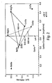
- Potential well layer materials and thicknesses are typically chosen so as to provide a desired transition energy, which will correspond to the wavelength of light to be emitted from the quantum well. For example, the points labeled 460 nm, 540 nm and 630 nm in Fig.
- each quantum well layer represents Cd(Mg)ZnSe alloys having lattice constants close to that for an InP substrate (5.8687 Angstroms or 0.58687 nm) and band gap energies corresponding to wavelengths of 460nm (blue), 540nm (green) and 630nm (red).
- the potential well may be regarded as a quantum well.
- the thickness of each quantum well layer will determine the amount of quantization energy in the quantum well, which is added to the bulk band gap energy to determine the transition energy in the quantum well.
- the wavelength associated with each quantum well can be tuned by adjustment of the quantum well layer thickness.
- thicknesses for quantum well layers are between 1 nm and 100 nm, more typically between 2 nm and 35 nm.
- the quantization energy translates into a reduction in wavelength of 20 to 50 nm relative to that expected on the basis of the band gap energy alone.
- Strain in the emitting layer may also change the transition energy for potential wells and quantum wells, including the strain resulting from the imperfect match of lattice constants between pseudomorphic layers.
- the thickness of these additional layers is typically much greater than that for the potential wells, typically at least 50 nm and up to 100 ⁇ m.
- any suitable emission wavelengths may be chosen, including those in the infrared, visible, and ultraviolet bands.
- the emission wavelengths are chosen so that the combined output of light emitted by the device creates the appearance of any color that can be generated by the combination of two, three or more monochromatic light sources, including white or near-white colors, pastel colors, magenta, cyan, and the like.
- the semiconductor device according to the present invention emits light at an invisible infrared or ultraviolet wavelength and at a visible wavelength as an indication that the device is in operation.
- the first potential well is associated with the highest transition energy (shortest wavelength), so that photons emitted from the first potential well have sufficient energy to drive other potential wells.
- Fig. 1 is a band diagram representing conduction and valence bands of semiconductors in a construction according to one embodiment of the present invention. Layer thickness is not represented to scale. Table I indicates the composition of layers 1-14 in this embodiment and the band gap energy (Eg) for that composition. Table I Layer Composition Band gap Energy (E g ) 1 InP substrate 1.35 eV 2 n-doped Cd 0.24 Mg 0.43 Zn 0.33 Se 2.9 eV 3 Cd 0.35 Mg 0.27 Zn 0.38 Se 2.6 eV 4 Cd 0 .
- Layers 10,11,12,13 and 14 represent a pn junction, or, more specifically, a pin junction, since intermediate undoped ("intrinsic" doping) layers 11,12 and 13 are interposed between n-doped layer 10 and p-doped layer 14.
- Layer 12 represents a single potential well within the pn junction which is a quantum well having a thickness of about 10 nm. Alternately, the device may comprise multiple potential or quantum wells within the pn junction.
- Layers 8 and 4 represent second and third potential wells not within a pn junction, each being a quantum well having a thickness of about 10 nm. Alternately, the device may comprise additional potential or quantum wells not within the pn junction.
- the device may comprise a single potential or quantum well not within the pn junction.
- Layers 3, 5, 7 and 9 represent absorbing layers, each having a thickness of about 1000 nm.
- Electrical contacts, not shown, provide a path for supply of electrical current to the pn junction. Electrical contacts conduct electricity and typically are composed of conductive metal. The positive electrical contact is electrically connected, either directly or indirectly through intermediate structures, to layer 14. The negative electrical contact is electrically connected, either directly or indirectly through intermediate structures, to one or more of layers 1, 2, 3, 4, 5, 6, 7, 8, 9 or 10.
- this embodiment of the present invention operates according to the following principles: When an electrical current passes from layer 14 to layer 10, blue-wavelength photons are emitted from quantum well (12) in the pn junction. Photons traveling in the direction of layer 14 may leave the device. Photons traveling in the opposite direction may be absorbed and reemitted from the second quantum well (8) as green-wavelength photons or from the third quantum well (4) as red-wavelength photons. The absorption of a blue-wavelength photon generates an electron-hole pair which may then recombine in the second or third quantum wells, with the emission of a photon. Green- or redwavelength photons traveling in the direction of layer 14 may leave the device.
- the polychromatic combination of blue-, green- and red-wavelength light emitted from the device may appear white or near-white in color.
- the intensity of blue-, green- and red-wavelength light emitted from the device may be balanced in any suitable manner, including manipulation of the number of potential wells of each type and the use of filters or reflective layers.
- Fig. 3 represents a spectrum of light that emits from one embodiment of the device according to the present invention.
- absorbing layers 3, 5, 7 and 9 may be especially suitable to absorb photons emitted from the first quantum well (12), since they have a band gap energy that is intermediate between the transition energy of the first quantum well (12) and those of the second and third quantum wells (8 and 4). Electron-hole pairs generated by absorption of photons in the absorbing layers 3, 5, 7 and 9 are typically captured by the second or third quantum wells 8 and 4 before recombining with concomitant emission of a photon.
- Absorbing layers may optionally be doped, typically like to surrounding layers, which in this embodiment would be n-doping. Absorbing layers may optionally have a gradient in composition over all or a portion of their thickness, so as to funnel or direct electrons and/or holes toward potential wells.
- the semiconductor device according to the present invention may comprise additional layers of conducting, semiconducting or non-conducting materials.
- Electrical contact layers may be added to provide a path for supply of electrical current to the pn junction of the LED. Electrical contact layers may be placed such that the current supplied to the pn junction passes also through the potential wells that are not in the pn junction, or such that the current does not pass through potential wells that are not in the pn junction.
- Light filtering layers may be added to alter or correct the balance of light wavelengths in the light emitted by the device.
- layers comprising a mirror or reflector may be added behind the LED element, e.g., between the substrate and LED element, behind the substrate and LED element, within or comprising the substrate, or behind the LED after removal of the substrate.
- the semiconductor device according to the present invention is a white or near-white LED which emits light at four principal wavelengths in the blue, green, yellow and red bands. In one embodiment, the semiconductor device according to the present invention is a white or near-white LED which emits light at two principal wavelengths in the blue and yellow bands.
- the semiconductor device according to the present invention may comprise additional semiconductor elements comprising active or passive components such as resistors, diodes, zener diodes, conventional LED's, capacitors, transistors, bipolar transistors, FET transistors, MOSFET transistors, insulated gate bipolar transistors, phototransistors, photodetectors, SCR's, thyristors, triacs, voltage regulators, and other circuit elements.
- the semiconductor device according to the present invention may comprise an integrated circuit.
- the semiconductor device according to the present invention may comprise a display panel or an illumination panel.
- the layered construction according to the present invention may be manufactured by any suitable method, which may include molecular beam epitaxy (MBE), chemical vapor deposition, liquid phase epitaxy and vapor phase epitaxy.
- MBE molecular beam epitaxy
- chemical vapor deposition liquid phase epitaxy
- vapor phase epitaxy vapor phase epitaxy
- the semiconductor device may be a component or the critical component of a graphic display device such as a large- or small-screen video monitor, computer monitor or display, television, telephone device or telephone device display, personal digital assistant or personal digital assistant display, pager or pager display, calculator or calculator display, game or game display, toy or toy display, large or small appliance or large or small appliance display, automotive dashboard or automotive dashboard display, automotive interior or automotive interior display, marine dashboard or marine dashboard display, marine interior or marine interior display, aeronautic dashboard or aeronautic dashboard display, aeronautic interior or aeronautic interior display, traffic control device or traffic control device display, advertising display, advertising sign, or the like.
- a graphic display device such as a large- or small-screen video monitor, computer monitor or display, television, telephone device or telephone device display, personal digital assistant or personal digital assistant display, pager or pager display, calculator or calculator display, game or game display, toy or toy display, large or small appliance or large or small appliance display, automotive dashboard or automotive dashboard display, automotive interior or automotive interior display, marine dashboard or marine
- the semiconductor device according to the present invention may be a component or the critical component of a liquid crystal display (LCD), or like display, as a backlight to that display.
- the semiconductor device according to the present invention is specially adapted for use as a backlight for a liquid crystal display by matching the colors emitted by the semiconductor device according to the present invention to the color filters of the LCD display.
- the semiconductor device according to the present invention may be a component or the critical component of an illumination device such as a free-standing or built-in lighting fixture or lamp, landscape or architectural illumination fixture, handheld or vehicle-mounted lamp, automotive headlight or taillight, automotive interior illumination fixture, automotive or non-automotive signaling device, road illumination device, traffic control signaling device, marine lamp or signaling device or interior illumination fixture, aeronautic lamp or signaling device or interior illumination fixture, large or small appliance or large or small appliance lamp, or the like; or any device or component used as a source of infrared, visible, or ultraviolet radiation.
- an illumination device such as a free-standing or built-in lighting fixture or lamp, landscape or architectural illumination fixture, handheld or vehicle-mounted lamp, automotive headlight or taillight, automotive interior illumination fixture, automotive or non-automotive signaling device, road illumination device, traffic control signaling device, marine lamp or signaling device or interior illumination fixture, aeronautic lamp or signaling device or interior illumination fixture, large or small appliance or large or small appliance lamp, or the like; or any device or
Landscapes
- Chemical & Material Sciences (AREA)
- Engineering & Computer Science (AREA)
- Nanotechnology (AREA)
- Physics & Mathematics (AREA)
- Life Sciences & Earth Sciences (AREA)
- Biophysics (AREA)
- Optics & Photonics (AREA)
- Crystallography & Structural Chemistry (AREA)
- Led Devices (AREA)
Applications Claiming Priority (2)
| Application Number | Priority Date | Filing Date | Title |
|---|---|---|---|
| US11/009,241 US7745814B2 (en) | 2004-12-09 | 2004-12-09 | Polychromatic LED's and related semiconductor devices |
| PCT/US2005/029852 WO2006062560A1 (en) | 2004-12-09 | 2005-08-22 | Polychromatic led's and related semiconductor devices |
Publications (2)
| Publication Number | Publication Date |
|---|---|
| EP1825526A1 EP1825526A1 (en) | 2007-08-29 |
| EP1825526B1 true EP1825526B1 (en) | 2008-10-15 |
Family
ID=36046862
Family Applications (1)
| Application Number | Title | Priority Date | Filing Date |
|---|---|---|---|
| EP05791694A Expired - Lifetime EP1825526B1 (en) | 2004-12-09 | 2005-08-22 | Polychromatic led's and related semiconductor devices |
Country Status (8)
| Country | Link |
|---|---|
| US (2) | US7745814B2 (enExample) |
| EP (1) | EP1825526B1 (enExample) |
| JP (2) | JP2008523612A (enExample) |
| KR (1) | KR101180248B1 (enExample) |
| CN (1) | CN100557830C (enExample) |
| AT (1) | ATE411620T1 (enExample) |
| DE (1) | DE602005010475D1 (enExample) |
| WO (1) | WO2006062560A1 (enExample) |
Families Citing this family (38)
| Publication number | Priority date | Publication date | Assignee | Title |
|---|---|---|---|---|
| US7719015B2 (en) * | 2004-12-09 | 2010-05-18 | 3M Innovative Properties Company | Type II broadband or polychromatic LED's |
| US7745814B2 (en) * | 2004-12-09 | 2010-06-29 | 3M Innovative Properties Company | Polychromatic LED's and related semiconductor devices |
| US7402831B2 (en) * | 2004-12-09 | 2008-07-22 | 3M Innovative Properties Company | Adapting short-wavelength LED's for polychromatic, broadband, or “white” emission |
| US7952110B2 (en) * | 2006-06-12 | 2011-05-31 | 3M Innovative Properties Company | LED device with re-emitting semiconductor construction and converging optical element |
| US7863634B2 (en) * | 2006-06-12 | 2011-01-04 | 3M Innovative Properties Company | LED device with re-emitting semiconductor construction and reflector |
| KR20090018623A (ko) * | 2006-06-12 | 2009-02-20 | 쓰리엠 이노베이티브 프로퍼티즈 컴파니 | 재발광 반도체 구성 및 수렴 광학 요소를 갖는 led 소자 |
| US20070284565A1 (en) * | 2006-06-12 | 2007-12-13 | 3M Innovative Properties Company | Led device with re-emitting semiconductor construction and optical element |
| US7902542B2 (en) * | 2006-06-14 | 2011-03-08 | 3M Innovative Properties Company | Adapted LED device with re-emitting semiconductor construction |
| US7717599B2 (en) * | 2006-07-31 | 2010-05-18 | 3M Innovative Properties Company | Integrating light source module |
| US20080051135A1 (en) * | 2006-07-31 | 2008-02-28 | 3M Innovative Properties Company | Combination camera/projector system |
| EP2050147A2 (en) | 2006-07-31 | 2009-04-22 | 3M Innovative Properties Company | Led source with hollow collection lens |
| KR20090034369A (ko) | 2006-07-31 | 2009-04-07 | 쓰리엠 이노베이티브 프로퍼티즈 컴파니 | 광학 투사 서브시스템 |
| US8075140B2 (en) * | 2006-07-31 | 2011-12-13 | 3M Innovative Properties Company | LED illumination system with polarization recycling |
| US20080036972A1 (en) * | 2006-07-31 | 2008-02-14 | 3M Innovative Properties Company | Led mosaic |
| JP2010525555A (ja) * | 2007-03-08 | 2010-07-22 | スリーエム イノベイティブ プロパティズ カンパニー | 発光素子のアレイ |
| EP2160645A2 (en) | 2007-05-20 | 2010-03-10 | 3M Innovative Properties Company | Light recycling hollow cavity type display backlight |
| TWI439641B (zh) * | 2007-05-20 | 2014-06-01 | 3M Innovative Properties Co | 用於側面發光型背光之準直光注入器 |
| WO2008144636A2 (en) | 2007-05-20 | 2008-11-27 | 3M Innovative Properties Company | Design parameters for thin hollow cavity backlights of the light-recycling type |
| JP2010528432A (ja) * | 2007-05-20 | 2010-08-19 | スリーエム イノベイティブ プロパティズ カンパニー | カラーled光源を効率的に利用した白色光バックライト及び類似製品 |
| WO2008144644A2 (en) | 2007-05-20 | 2008-11-27 | 3M Innovative Properties Company | Semi-specular components in hollow cavity light recycling backlights |
| CN101939855B (zh) * | 2007-12-10 | 2013-10-30 | 3M创新有限公司 | 半导体发光装置及其制造方法 |
| EP2255231A1 (en) * | 2008-02-07 | 2010-12-01 | 3M Innovative Properties Company | Hollow backlight with structured films |
| JP5792464B2 (ja) * | 2008-02-22 | 2015-10-14 | スリーエム イノベイティブ プロパティズ カンパニー | 選択的出力光束分布を有するバックライト及びそれを使用した表示システム並びにバックライトの形成方法 |
| EP2297607B1 (en) * | 2008-06-04 | 2014-04-23 | 3M Innovative Properties Company | Hollow backlight with tilted light source |
| KR20110019390A (ko) * | 2008-06-05 | 2011-02-25 | 쓰리엠 이노베이티브 프로퍼티즈 컴파니 | 접합형 반도체 파장 변환기를 갖는 발광 다이오드 |
| JP2011526074A (ja) * | 2008-06-26 | 2011-09-29 | スリーエム イノベイティブ プロパティズ カンパニー | 半導体光変換構成体 |
| US8591052B2 (en) * | 2008-10-27 | 2013-11-26 | 3M Innovative Properties Company | Semispecular hollow backlight with gradient extraction |
| US8192048B2 (en) * | 2009-04-22 | 2012-06-05 | 3M Innovative Properties Company | Lighting assemblies and systems |
| CN102668044A (zh) * | 2009-11-18 | 2012-09-12 | 3M创新有限公司 | 用于ii-vi族半导体的新型湿蚀刻剂及方法 |
| WO2011153141A2 (en) * | 2010-06-03 | 2011-12-08 | 3M Innovative Properties Company | Light converting and emitting device with suppressed dark-line defects |
| US8975614B2 (en) * | 2011-08-23 | 2015-03-10 | Micron Technology, Inc. | Wavelength converters for solid state lighting devices, and associated systems and methods |
| US9331252B2 (en) | 2011-08-23 | 2016-05-03 | Micron Technology, Inc. | Wavelength converters, including polarization-enhanced carrier capture converters, for solid state lighting devices, and associated systems and methods |
| KR102019858B1 (ko) * | 2013-07-18 | 2019-09-09 | 엘지이노텍 주식회사 | 발광소자 및 조명시스템 |
| DE102017103856A1 (de) | 2017-02-24 | 2018-08-30 | Osram Opto Semiconductors Gmbh | Optoelektronischer Halbleiterchip |
| KR102809724B1 (ko) * | 2020-03-27 | 2025-05-21 | 구글 엘엘씨 | 변형이 감소된 인듐 갈륨 질화물 발광 다이오드 |
| US20220181516A1 (en) * | 2020-12-04 | 2022-06-09 | Seoul Viosys Co., Ltd. | Mixed color light emitting device |
| CN115274949A (zh) * | 2022-07-22 | 2022-11-01 | 厦门士兰明镓化合物半导体有限公司 | 一种发光二极管及其制备方法 |
| CN115360274A (zh) * | 2022-07-22 | 2022-11-18 | 厦门士兰明镓化合物半导体有限公司 | 一种发光二极管及其制备方法 |
Family Cites Families (58)
| Publication number | Priority date | Publication date | Assignee | Title |
|---|---|---|---|---|
| US4527179A (en) | 1981-02-09 | 1985-07-02 | Semiconductor Energy Laboratory Co., Ltd. | Non-single-crystal light emitting semiconductor device |
| FR2538171B1 (fr) | 1982-12-21 | 1986-02-28 | Thomson Csf | Diode electroluminescente a emission de surface |
| US4688068A (en) * | 1983-07-08 | 1987-08-18 | The United States Of America As Represented By The Department Of Energy | Quantum well multijunction photovoltaic cell |
| JPH06244506A (ja) | 1993-02-19 | 1994-09-02 | Sony Corp | 半導体表示装置及びその製造方法 |
| US5459337A (en) * | 1993-02-19 | 1995-10-17 | Sony Corporation | Semiconductor display device with red, green and blue emission |
| JPH06268331A (ja) | 1993-03-11 | 1994-09-22 | Toshiba Corp | 半導体発光装置 |
| JP2991616B2 (ja) * | 1994-06-30 | 1999-12-20 | シャープ株式会社 | 半導体発光素子 |
| US5646419A (en) | 1995-04-07 | 1997-07-08 | California Institute Of Technology | n-type wide bandgap semiconductors grown on a p-type layer to form hole injection pn heterojunctions and methods of fabricating the same |
| DE19542241C2 (de) | 1995-11-13 | 2003-01-09 | Siemens Ag | Optoelektronisches Bauelement in II-VI-Halbleitermaterial |
| JPH09181398A (ja) | 1995-12-25 | 1997-07-11 | Sony Corp | 半導体発光素子 |
| US5889295A (en) | 1996-02-26 | 1999-03-30 | Kabushiki Kaisha Toshiba | Semiconductor device |
| US5684309A (en) | 1996-07-11 | 1997-11-04 | North Carolina State University | Stacked quantum well aluminum indium gallium nitride light emitting diodes |
| TW383508B (en) | 1996-07-29 | 2000-03-01 | Nichia Kagaku Kogyo Kk | Light emitting device and display |
| DE19703615A1 (de) | 1997-01-31 | 1998-08-06 | Siemens Ag | Optoelektronisches Halbleiterbauelement |
| DE19729396A1 (de) | 1997-07-09 | 1999-01-14 | Siemens Ag | Elektrischer Kontakt für ein II-VI-Halbleiterbauelement und Verfahren zum Herstellen des elektrischen Kontaktes |
| US6214116B1 (en) * | 1998-01-17 | 2001-04-10 | Hanvac Corporation | Horizontal reactor for compound semiconductor growth |
| JP3559446B2 (ja) | 1998-03-23 | 2004-09-02 | 株式会社東芝 | 半導体発光素子および半導体発光装置 |
| EP0954034A3 (en) * | 1998-04-28 | 2000-01-26 | Canare Electric Co., Ltd. | Light receiving device with quantum-wave interference layers |
| TW406442B (en) | 1998-07-09 | 2000-09-21 | Sumitomo Electric Industries | White colored LED and intermediate colored LED |
| US5988925A (en) * | 1998-10-26 | 1999-11-23 | Baggett; R. Sherman | Stacked paper fastener |
| CN1070315C (zh) * | 1998-11-06 | 2001-08-29 | 吉林大学 | 有机多量子阱结构白光电致发光器件 |
| US6252896B1 (en) * | 1999-03-05 | 2001-06-26 | Agilent Technologies, Inc. | Long-Wavelength VCSEL using buried bragg reflectors |
| US6303404B1 (en) | 1999-05-28 | 2001-10-16 | Yong Tae Moon | Method for fabricating white light emitting diode using InGaN phase separation |
| WO2000076005A1 (en) | 1999-06-04 | 2000-12-14 | Trustees Of Boston University | Photon recycling semiconductor multi-wavelength light-emitting diodes |
| DE19952932C1 (de) | 1999-11-03 | 2001-05-03 | Osram Opto Semiconductors Gmbh | LED-Weißlichtquelle mit breitbandiger Anregung |
| US6504171B1 (en) | 2000-01-24 | 2003-01-07 | Lumileds Lighting, U.S., Llc | Chirped multi-well active region LED |
| JP3486900B2 (ja) | 2000-02-15 | 2004-01-13 | ソニー株式会社 | 発光装置およびそれを用いた光装置 |
| AU2001252894A1 (en) | 2000-03-06 | 2001-09-17 | Teledyne Lighting And Display Products, Inc. | Lighting apparatus having quantum dot layer |
| JP4008656B2 (ja) | 2000-12-27 | 2007-11-14 | 株式会社東芝 | 半導体発光装置 |
| TW497277B (en) * | 2000-03-10 | 2002-08-01 | Toshiba Corp | Semiconductor light emitting device and method for manufacturing the same |
| KR100382481B1 (ko) | 2000-06-09 | 2003-05-01 | 엘지전자 주식회사 | 백색 발광 다이오드 소자 및 그 제조 방법 |
| DE10036940A1 (de) * | 2000-07-28 | 2002-02-07 | Patent Treuhand Ges Fuer Elektrische Gluehlampen Mbh | Lumineszenz-Konversions-LED |
| JP2002217456A (ja) | 2001-01-19 | 2002-08-02 | Ngk Insulators Ltd | 半導体発光素子 |
| JP2002222989A (ja) * | 2001-01-26 | 2002-08-09 | Toshiba Corp | 半導体発光素子 |
| US6711194B2 (en) | 2001-02-08 | 2004-03-23 | The Furukawa Electric Co., Ltd. | High output power semiconductor laser diode |
| KR100422944B1 (ko) | 2001-05-31 | 2004-03-12 | 삼성전기주식회사 | 반도체 엘이디(led) 소자 |
| JP3791765B2 (ja) | 2001-06-08 | 2006-06-28 | 豊田合成株式会社 | Iii族窒化物系化合物半導体発光素子 |
| US6837605B2 (en) | 2001-11-28 | 2005-01-04 | Osram Opto Semiconductors Gmbh | Led illumination system |
| US6711195B2 (en) | 2002-02-28 | 2004-03-23 | Agilent Technologies, Inc. | Long-wavelength photonic device with GaAsSb quantum-well layer |
| US6831306B1 (en) * | 2002-03-06 | 2004-12-14 | Daktronics, Inc. | Extended length light emitting diode |
| US6838605B2 (en) * | 2002-04-15 | 2005-01-04 | Remo, Inc. | Drumshell laminate |
| CA2427559A1 (en) | 2002-05-15 | 2003-11-15 | Sumitomo Electric Industries, Ltd. | White color light emitting device |
| JP2004047748A (ja) | 2002-07-12 | 2004-02-12 | Stanley Electric Co Ltd | 発光ダイオード |
| JP2004072047A (ja) | 2002-08-09 | 2004-03-04 | Sumitomo Electric Ind Ltd | 白色発光素子、白色発光素子用基板および白色発光素子用基板の製造方法 |
| US6791104B2 (en) | 2002-09-26 | 2004-09-14 | Wisconsin Alumni Research Foundation | Type II quantum well optoelectronic devices |
| MY149573A (en) * | 2002-10-16 | 2013-09-13 | Nichia Corp | Oxynitride phosphor and production process thereof, and light-emitting device using oxynitride phosphor |
| TW591811B (en) | 2003-01-02 | 2004-06-11 | Epitech Technology Corp Ltd | Color mixing light emitting diode |
| JP3717480B2 (ja) | 2003-01-27 | 2005-11-16 | ローム株式会社 | 半導体発光装置 |
| TWI289937B (en) | 2003-03-04 | 2007-11-11 | Topco Scient Co Ltd | White light LED |
| EP1475835A3 (en) | 2003-04-14 | 2004-12-15 | Epitech Corporation, Ltd. | Color mixing light emitting diode |
| US7126160B2 (en) * | 2004-06-18 | 2006-10-24 | 3M Innovative Properties Company | II-VI/III-V layered construction on InP substrate |
| US7223998B2 (en) | 2004-09-10 | 2007-05-29 | The Regents Of The University Of California | White, single or multi-color light emitting diodes by recycling guided modes |
| JP4291239B2 (ja) * | 2004-09-10 | 2009-07-08 | エルピーダメモリ株式会社 | 半導体記憶装置及びテスト方法 |
| US20060081858A1 (en) * | 2004-10-14 | 2006-04-20 | Chung-Hsiang Lin | Light emitting device with omnidirectional reflectors |
| US7402831B2 (en) * | 2004-12-09 | 2008-07-22 | 3M Innovative Properties Company | Adapting short-wavelength LED's for polychromatic, broadband, or “white” emission |
| US7745814B2 (en) * | 2004-12-09 | 2010-06-29 | 3M Innovative Properties Company | Polychromatic LED's and related semiconductor devices |
| US7719015B2 (en) * | 2004-12-09 | 2010-05-18 | 3M Innovative Properties Company | Type II broadband or polychromatic LED's |
| US9018619B2 (en) * | 2006-10-09 | 2015-04-28 | Cree, Inc. | Quantum wells for light conversion |
-
2004
- 2004-12-09 US US11/009,241 patent/US7745814B2/en not_active Expired - Fee Related
-
2005
- 2005-08-22 CN CNB2005800425034A patent/CN100557830C/zh not_active Expired - Fee Related
- 2005-08-22 WO PCT/US2005/029852 patent/WO2006062560A1/en not_active Ceased
- 2005-08-22 AT AT05791694T patent/ATE411620T1/de not_active IP Right Cessation
- 2005-08-22 KR KR1020077015505A patent/KR101180248B1/ko not_active Expired - Fee Related
- 2005-08-22 EP EP05791694A patent/EP1825526B1/en not_active Expired - Lifetime
- 2005-08-22 JP JP2007545439A patent/JP2008523612A/ja not_active Withdrawn
- 2005-08-22 DE DE602005010475T patent/DE602005010475D1/de not_active Expired - Lifetime
-
2010
- 2010-05-17 US US12/781,227 patent/US8148741B2/en not_active Expired - Fee Related
-
2011
- 2011-05-18 JP JP2011111294A patent/JP2011187977A/ja active Pending
Also Published As
| Publication number | Publication date |
|---|---|
| EP1825526A1 (en) | 2007-08-29 |
| CN101076898A (zh) | 2007-11-21 |
| CN100557830C (zh) | 2009-11-04 |
| KR101180248B1 (ko) | 2012-09-05 |
| JP2008523612A (ja) | 2008-07-03 |
| JP2011187977A (ja) | 2011-09-22 |
| WO2006062560A1 (en) | 2006-06-15 |
| US20100224889A1 (en) | 2010-09-09 |
| US20060124918A1 (en) | 2006-06-15 |
| DE602005010475D1 (de) | 2008-11-27 |
| ATE411620T1 (de) | 2008-10-15 |
| US7745814B2 (en) | 2010-06-29 |
| US8148741B2 (en) | 2012-04-03 |
| KR20070089218A (ko) | 2007-08-30 |
Similar Documents
| Publication | Publication Date | Title |
|---|---|---|
| EP1825526B1 (en) | Polychromatic led's and related semiconductor devices | |
| US7700938B2 (en) | Adapting short-wavelength LED's for polychromatic, broadband, or “white” emission | |
| US8148742B2 (en) | Type II broadband or polychromatic LEDs | |
| US7902542B2 (en) | Adapted LED device with re-emitting semiconductor construction | |
| KR20230028202A (ko) | 단일칩 복수 대역 발광 다이오드 및 그 응용품 |
Legal Events
| Date | Code | Title | Description |
|---|---|---|---|
| PUAI | Public reference made under article 153(3) epc to a published international application that has entered the european phase |
Free format text: ORIGINAL CODE: 0009012 |
|
| 17P | Request for examination filed |
Effective date: 20070607 |
|
| AK | Designated contracting states |
Kind code of ref document: A1 Designated state(s): AT BE BG CH CY CZ DE DK EE ES FI FR GB GR HU IE IS IT LI LT LU LV MC NL PL PT RO SE SI SK TR |
|
| DAX | Request for extension of the european patent (deleted) | ||
| GRAP | Despatch of communication of intention to grant a patent |
Free format text: ORIGINAL CODE: EPIDOSNIGR1 |
|
| GRAS | Grant fee paid |
Free format text: ORIGINAL CODE: EPIDOSNIGR3 |
|
| GRAA | (expected) grant |
Free format text: ORIGINAL CODE: 0009210 |
|
| AK | Designated contracting states |
Kind code of ref document: B1 Designated state(s): AT BE BG CH CY CZ DE DK EE ES FI FR GB GR HU IE IS IT LI LT LU LV MC NL PL PT RO SE SI SK TR |
|
| REG | Reference to a national code |
Ref country code: CH Ref legal event code: EP Ref country code: GB Ref legal event code: FG4D |
|
| REG | Reference to a national code |
Ref country code: IE Ref legal event code: FG4D |
|
| REF | Corresponds to: |
Ref document number: 602005010475 Country of ref document: DE Date of ref document: 20081127 Kind code of ref document: P |
|
| PG25 | Lapsed in a contracting state [announced via postgrant information from national office to epo] |
Ref country code: AT Free format text: LAPSE BECAUSE OF FAILURE TO SUBMIT A TRANSLATION OF THE DESCRIPTION OR TO PAY THE FEE WITHIN THE PRESCRIBED TIME-LIMIT Effective date: 20081015 Ref country code: BG Free format text: LAPSE BECAUSE OF FAILURE TO SUBMIT A TRANSLATION OF THE DESCRIPTION OR TO PAY THE FEE WITHIN THE PRESCRIBED TIME-LIMIT Effective date: 20090115 Ref country code: ES Free format text: LAPSE BECAUSE OF FAILURE TO SUBMIT A TRANSLATION OF THE DESCRIPTION OR TO PAY THE FEE WITHIN THE PRESCRIBED TIME-LIMIT Effective date: 20090126 Ref country code: LT Free format text: LAPSE BECAUSE OF FAILURE TO SUBMIT A TRANSLATION OF THE DESCRIPTION OR TO PAY THE FEE WITHIN THE PRESCRIBED TIME-LIMIT Effective date: 20081015 |
|
| PG25 | Lapsed in a contracting state [announced via postgrant information from national office to epo] |
Ref country code: SI Free format text: LAPSE BECAUSE OF FAILURE TO SUBMIT A TRANSLATION OF THE DESCRIPTION OR TO PAY THE FEE WITHIN THE PRESCRIBED TIME-LIMIT Effective date: 20081015 Ref country code: PT Free format text: LAPSE BECAUSE OF FAILURE TO SUBMIT A TRANSLATION OF THE DESCRIPTION OR TO PAY THE FEE WITHIN THE PRESCRIBED TIME-LIMIT Effective date: 20090316 Ref country code: FI Free format text: LAPSE BECAUSE OF FAILURE TO SUBMIT A TRANSLATION OF THE DESCRIPTION OR TO PAY THE FEE WITHIN THE PRESCRIBED TIME-LIMIT Effective date: 20081015 Ref country code: IS Free format text: LAPSE BECAUSE OF FAILURE TO SUBMIT A TRANSLATION OF THE DESCRIPTION OR TO PAY THE FEE WITHIN THE PRESCRIBED TIME-LIMIT Effective date: 20090215 Ref country code: PL Free format text: LAPSE BECAUSE OF FAILURE TO SUBMIT A TRANSLATION OF THE DESCRIPTION OR TO PAY THE FEE WITHIN THE PRESCRIBED TIME-LIMIT Effective date: 20081015 Ref country code: LV Free format text: LAPSE BECAUSE OF FAILURE TO SUBMIT A TRANSLATION OF THE DESCRIPTION OR TO PAY THE FEE WITHIN THE PRESCRIBED TIME-LIMIT Effective date: 20081015 |
|
| PG25 | Lapsed in a contracting state [announced via postgrant information from national office to epo] |
Ref country code: EE Free format text: LAPSE BECAUSE OF FAILURE TO SUBMIT A TRANSLATION OF THE DESCRIPTION OR TO PAY THE FEE WITHIN THE PRESCRIBED TIME-LIMIT Effective date: 20081015 Ref country code: BE Free format text: LAPSE BECAUSE OF FAILURE TO SUBMIT A TRANSLATION OF THE DESCRIPTION OR TO PAY THE FEE WITHIN THE PRESCRIBED TIME-LIMIT Effective date: 20081015 Ref country code: RO Free format text: LAPSE BECAUSE OF FAILURE TO SUBMIT A TRANSLATION OF THE DESCRIPTION OR TO PAY THE FEE WITHIN THE PRESCRIBED TIME-LIMIT Effective date: 20081015 Ref country code: DK Free format text: LAPSE BECAUSE OF FAILURE TO SUBMIT A TRANSLATION OF THE DESCRIPTION OR TO PAY THE FEE WITHIN THE PRESCRIBED TIME-LIMIT Effective date: 20081015 |
|
| PLBE | No opposition filed within time limit |
Free format text: ORIGINAL CODE: 0009261 |
|
| STAA | Information on the status of an ep patent application or granted ep patent |
Free format text: STATUS: NO OPPOSITION FILED WITHIN TIME LIMIT |
|
| PG25 | Lapsed in a contracting state [announced via postgrant information from national office to epo] |
Ref country code: SE Free format text: LAPSE BECAUSE OF FAILURE TO SUBMIT A TRANSLATION OF THE DESCRIPTION OR TO PAY THE FEE WITHIN THE PRESCRIBED TIME-LIMIT Effective date: 20090115 Ref country code: IT Free format text: LAPSE BECAUSE OF FAILURE TO SUBMIT A TRANSLATION OF THE DESCRIPTION OR TO PAY THE FEE WITHIN THE PRESCRIBED TIME-LIMIT Effective date: 20081015 Ref country code: CZ Free format text: LAPSE BECAUSE OF FAILURE TO SUBMIT A TRANSLATION OF THE DESCRIPTION OR TO PAY THE FEE WITHIN THE PRESCRIBED TIME-LIMIT Effective date: 20081015 |
|
| 26N | No opposition filed |
Effective date: 20090716 |
|
| PG25 | Lapsed in a contracting state [announced via postgrant information from national office to epo] |
Ref country code: SK Free format text: LAPSE BECAUSE OF FAILURE TO SUBMIT A TRANSLATION OF THE DESCRIPTION OR TO PAY THE FEE WITHIN THE PRESCRIBED TIME-LIMIT Effective date: 20081015 |
|
| PG25 | Lapsed in a contracting state [announced via postgrant information from national office to epo] |
Ref country code: MC Free format text: LAPSE BECAUSE OF NON-PAYMENT OF DUE FEES Effective date: 20090831 |
|
| REG | Reference to a national code |
Ref country code: CH Ref legal event code: PL |
|
| GBPC | Gb: european patent ceased through non-payment of renewal fee |
Effective date: 20090822 |
|
| PG25 | Lapsed in a contracting state [announced via postgrant information from national office to epo] |
Ref country code: LI Free format text: LAPSE BECAUSE OF NON-PAYMENT OF DUE FEES Effective date: 20090831 Ref country code: CH Free format text: LAPSE BECAUSE OF NON-PAYMENT OF DUE FEES Effective date: 20090831 |
|
| REG | Reference to a national code |
Ref country code: FR Ref legal event code: ST Effective date: 20100430 |
|
| PG25 | Lapsed in a contracting state [announced via postgrant information from national office to epo] |
Ref country code: IE Free format text: LAPSE BECAUSE OF NON-PAYMENT OF DUE FEES Effective date: 20090822 Ref country code: FR Free format text: LAPSE BECAUSE OF NON-PAYMENT OF DUE FEES Effective date: 20090831 |
|
| PG25 | Lapsed in a contracting state [announced via postgrant information from national office to epo] |
Ref country code: GR Free format text: LAPSE BECAUSE OF FAILURE TO SUBMIT A TRANSLATION OF THE DESCRIPTION OR TO PAY THE FEE WITHIN THE PRESCRIBED TIME-LIMIT Effective date: 20090116 |
|
| PG25 | Lapsed in a contracting state [announced via postgrant information from national office to epo] |
Ref country code: GB Free format text: LAPSE BECAUSE OF NON-PAYMENT OF DUE FEES Effective date: 20090822 |
|
| PG25 | Lapsed in a contracting state [announced via postgrant information from national office to epo] |
Ref country code: LU Free format text: LAPSE BECAUSE OF NON-PAYMENT OF DUE FEES Effective date: 20090822 |
|
| PG25 | Lapsed in a contracting state [announced via postgrant information from national office to epo] |
Ref country code: HU Free format text: LAPSE BECAUSE OF FAILURE TO SUBMIT A TRANSLATION OF THE DESCRIPTION OR TO PAY THE FEE WITHIN THE PRESCRIBED TIME-LIMIT Effective date: 20090416 |
|
| PG25 | Lapsed in a contracting state [announced via postgrant information from national office to epo] |
Ref country code: TR Free format text: LAPSE BECAUSE OF FAILURE TO SUBMIT A TRANSLATION OF THE DESCRIPTION OR TO PAY THE FEE WITHIN THE PRESCRIBED TIME-LIMIT Effective date: 20081015 |
|
| PG25 | Lapsed in a contracting state [announced via postgrant information from national office to epo] |
Ref country code: CY Free format text: LAPSE BECAUSE OF FAILURE TO SUBMIT A TRANSLATION OF THE DESCRIPTION OR TO PAY THE FEE WITHIN THE PRESCRIBED TIME-LIMIT Effective date: 20081015 |
|
| PGFP | Annual fee paid to national office [announced via postgrant information from national office to epo] |
Ref country code: NL Payment date: 20170814 Year of fee payment: 13 |
|
| PGFP | Annual fee paid to national office [announced via postgrant information from national office to epo] |
Ref country code: DE Payment date: 20170815 Year of fee payment: 13 |
|
| REG | Reference to a national code |
Ref country code: DE Ref legal event code: R119 Ref document number: 602005010475 Country of ref document: DE |
|
| REG | Reference to a national code |
Ref country code: NL Ref legal event code: MM Effective date: 20180901 |
|
| PG25 | Lapsed in a contracting state [announced via postgrant information from national office to epo] |
Ref country code: NL Free format text: LAPSE BECAUSE OF NON-PAYMENT OF DUE FEES Effective date: 20180901 |
|
| PG25 | Lapsed in a contracting state [announced via postgrant information from national office to epo] |
Ref country code: DE Free format text: LAPSE BECAUSE OF NON-PAYMENT OF DUE FEES Effective date: 20190301 |