EP1815554B1 - Kopplungsleitungen f]r einen yig-filter oder yig-oszillator und verfahren zur herstellung der kopplungsleitungen - Google Patents
Kopplungsleitungen f]r einen yig-filter oder yig-oszillator und verfahren zur herstellung der kopplungsleitungen Download PDFInfo
- Publication number
- EP1815554B1 EP1815554B1 EP05813554A EP05813554A EP1815554B1 EP 1815554 B1 EP1815554 B1 EP 1815554B1 EP 05813554 A EP05813554 A EP 05813554A EP 05813554 A EP05813554 A EP 05813554A EP 1815554 B1 EP1815554 B1 EP 1815554B1
- Authority
- EP
- European Patent Office
- Prior art keywords
- yig
- filter
- coupling
- line
- coupling line
- Prior art date
- Legal status (The legal status is an assumption and is not a legal conclusion. Google has not performed a legal analysis and makes no representation as to the accuracy of the status listed.)
- Expired - Lifetime
Links
Images
Classifications
-
- H—ELECTRICITY
- H01—ELECTRIC ELEMENTS
- H01P—WAVEGUIDES; RESONATORS, LINES, OR OTHER DEVICES OF THE WAVEGUIDE TYPE
- H01P1/00—Auxiliary devices
- H01P1/20—Frequency-selective devices, e.g. filters
- H01P1/215—Frequency-selective devices, e.g. filters using ferromagnetic material
- H01P1/218—Frequency-selective devices, e.g. filters using ferromagnetic material the ferromagnetic material acting as a frequency selective coupling element, e.g. YIG-filters
-
- Y—GENERAL TAGGING OF NEW TECHNOLOGICAL DEVELOPMENTS; GENERAL TAGGING OF CROSS-SECTIONAL TECHNOLOGIES SPANNING OVER SEVERAL SECTIONS OF THE IPC; TECHNICAL SUBJECTS COVERED BY FORMER USPC CROSS-REFERENCE ART COLLECTIONS [XRACs] AND DIGESTS
- Y10—TECHNICAL SUBJECTS COVERED BY FORMER USPC
- Y10T—TECHNICAL SUBJECTS COVERED BY FORMER US CLASSIFICATION
- Y10T29/00—Metal working
- Y10T29/42—Piezoelectric device making
-
- Y—GENERAL TAGGING OF NEW TECHNOLOGICAL DEVELOPMENTS; GENERAL TAGGING OF CROSS-SECTIONAL TECHNOLOGIES SPANNING OVER SEVERAL SECTIONS OF THE IPC; TECHNICAL SUBJECTS COVERED BY FORMER USPC CROSS-REFERENCE ART COLLECTIONS [XRACs] AND DIGESTS
- Y10—TECHNICAL SUBJECTS COVERED BY FORMER USPC
- Y10T—TECHNICAL SUBJECTS COVERED BY FORMER US CLASSIFICATION
- Y10T29/00—Metal working
- Y10T29/49—Method of mechanical manufacture
- Y10T29/49002—Electrical device making
- Y10T29/49005—Acoustic transducer
-
- Y—GENERAL TAGGING OF NEW TECHNOLOGICAL DEVELOPMENTS; GENERAL TAGGING OF CROSS-SECTIONAL TECHNOLOGIES SPANNING OVER SEVERAL SECTIONS OF THE IPC; TECHNICAL SUBJECTS COVERED BY FORMER USPC CROSS-REFERENCE ART COLLECTIONS [XRACs] AND DIGESTS
- Y10—TECHNICAL SUBJECTS COVERED BY FORMER USPC
- Y10T—TECHNICAL SUBJECTS COVERED BY FORMER US CLASSIFICATION
- Y10T29/00—Metal working
- Y10T29/49—Method of mechanical manufacture
- Y10T29/49002—Electrical device making
- Y10T29/4902—Electromagnet, transformer or inductor
-
- Y—GENERAL TAGGING OF NEW TECHNOLOGICAL DEVELOPMENTS; GENERAL TAGGING OF CROSS-SECTIONAL TECHNOLOGIES SPANNING OVER SEVERAL SECTIONS OF THE IPC; TECHNICAL SUBJECTS COVERED BY FORMER USPC CROSS-REFERENCE ART COLLECTIONS [XRACs] AND DIGESTS
- Y10—TECHNICAL SUBJECTS COVERED BY FORMER USPC
- Y10T—TECHNICAL SUBJECTS COVERED BY FORMER US CLASSIFICATION
- Y10T29/00—Metal working
- Y10T29/49—Method of mechanical manufacture
- Y10T29/49002—Electrical device making
- Y10T29/49117—Conductor or circuit manufacturing
- Y10T29/49121—Beam lead frame or beam lead device
-
- Y—GENERAL TAGGING OF NEW TECHNOLOGICAL DEVELOPMENTS; GENERAL TAGGING OF CROSS-SECTIONAL TECHNOLOGIES SPANNING OVER SEVERAL SECTIONS OF THE IPC; TECHNICAL SUBJECTS COVERED BY FORMER USPC CROSS-REFERENCE ART COLLECTIONS [XRACs] AND DIGESTS
- Y10—TECHNICAL SUBJECTS COVERED BY FORMER USPC
- Y10T—TECHNICAL SUBJECTS COVERED BY FORMER US CLASSIFICATION
- Y10T29/00—Metal working
- Y10T29/49—Method of mechanical manufacture
- Y10T29/49002—Electrical device making
- Y10T29/49117—Conductor or circuit manufacturing
- Y10T29/49124—On flat or curved insulated base, e.g., printed circuit, etc.
- Y10T29/49155—Manufacturing circuit on or in base
- Y10T29/49156—Manufacturing circuit on or in base with selective destruction of conductive paths
Definitions
- the invention relates to a YIG filter or a YIG oscillator.
- YIG band-pass filter or YIG oscillators have at least one resonator, which is preferably spherical and made of a yttrium iron garnet (Y ttrium- I RON G arnet YIG) is prepared.
- the Resonator Brady is mediated by coupling lines, which must be designed and arranged so that the center of the resonator and the center of the bending radius of a coupling line match exactly.
- a YIG bandpass filter with correspondingly formed coupling lines is for example from the document US 4,480,238 known.
- the tunable YIG bandpass filter in this case has a base body, which slots for receiving isolated platelets having at one edge a conductive coating which serves as coupling lines comprises. Furthermore, filter chambers are provided for receiving the YIG elements. The platelets are placed over the YIG elements in the slots so that the YIG elements are arranged in indentations in the edges provided with the conductive coating. The YIG elements and the plates are fixed in fixed positions.
- a disadvantage of the YIG bandpass filter known from the above-mentioned publication is, in particular, the complicated manufacture of the platelets forming the coupling lines.
- the serving as a carrier insulator must first be appropriately shaped and then provided with the conductive coating. This is expensive and prone to jeopardy because the coating is sensitive to damage due to the small layer thickness.
- Object of the present invention is to provide a YIG filter or YIG oscillator, with coupling lines that are easy to manufacture, insensitive to damage and easy to install.
- Figure 2 discloses a YIG arrangement according to the preamble of claim 1.
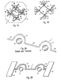
- Fig. 1A shows in a schematic, perspective view of an embodiment of a YIG bandpass filter 2, which has a base body 3 and in the embodiment, four formed in the base body 3 filter chambers 4 with as many YIG elements 6.
- the YIG elements 6 are spherically formed from an yttrium-iron garnet, mounted on holders 10, for example by gluing with epoxy resin and electromagnetically coupled by coupling lines 1.
- the filter chambers 4 are interconnected by slots 5, in which the coupling lines 1 are inserted.
- two of the filter chambers 4 are identical in the embodiment.
- the filter chambers 4 denoted by 4b have only the YIG elements 6.
- the number of filter chambers 4b is not limited to two, but may be one or more so that the total number of filter chambers 4 may be three or more.
- Fig. 1B shows for ease of understanding the arrangement of the coupling lines 1 and mounted on their holders 10 YIG elements 6 without the surrounding body.
- the coupling lines 1 are executed in the embodiment in two different forms.
- the filter chambers 4b interconnecting coupling line 1 is designed as input or output line 1a, while in the embodiment, three further coupling lines 1 are designed as connecting lines 1b.
- Fig. 1B shows, the coupling lines 1 on tabs 8, which serve on the one hand, the ground connection of the coupling lines 1 in the base body 3 and on the other hand, the fixation of the coupling lines 1 in the slots 5.
- the contact lugs 8 are rectangular in shape, wherein an edge length of the contact lugs 8 corresponds approximately to the axial thickness of the base body 2.
- FIGS. 2A and 2B is recognizable, whereby the coupling lines 1 according to Fig. 2B from conventional coupling lines 1 according to FIG Fig. 2A differ.
- the two embodiments have in common that in each case at least one curved portion 17 is provided, which surrounds a respective YIG element 6 so at least partially, that a center of the YIG element 6 coincides with a center of the curved portion 17. Furthermore, at least one line section 18 is provided.
- FIG. 2A shown coupling line 1 according to the prior art is bent from a wire.
- the YIG elements 6 in the in FIGS. 2A and 2B introduced basic body 3, not shown, and then inserted only roughly pre-bent wire in the slots 5.
- a measurement of the degree of coupling results where the coupling line 1 still needs to be bent. This is done manually by means of a suitable tool. Thereafter must be checked again and readjusted. For this purpose, each time the YIG filter 2 or YIG oscillator must be opened and then reassembled to make the measurement. The method is thus extremely complicated and often even leads to the fact that the workpiece must be completely discarded after several iterations, because no satisfactory coupling is achieved.
- the inventively designed coupling lines 1 according to Fig. 2B made of a metallic foil by suitable methods such as etching, eroding, cutting, in particular laser cutting or water jet cutting and / or punching and assembled. Thereafter, the correct positioning of the YIG elements 6 takes place relative to the coupling lines. 1
- the film is made of a copper-beryllium alloy to meet both the requirements of elasticity and strength.
- the thickness of the film is preferably about 50 microns.
- the preparation of the coupling lines 1 from the film takes place in several processing steps. First, the film is cleaned and applied on both sides with a positive resist at an alignment accuracy of about 5 microns in a layer thickness of about 5 microns to create a mask. Thereafter, the preparation of the coupling lines 1, for example, by spray etching with iron chloride. (FeCl 3) Subsequently, the liberated in the form of a carrier 9 with a predetermined number of coupling lines 1 of all paint residues and galvanically provided with a gold coating of about 5 microns. After that follows a curing process for example, one hour at 325 ° C. Then the coupling lines can be released from the film carrier 9 and installed.
- the coupling lines 1 have by the manufacturing method described a solid shape with a well-defined radius of curvature in the curved portions 17 at a uniform curvature.
- the YIG elements 6 are then aligned relative to the coupling lines 1. This is compared to the prior art simpler and associated with considerably less effort, because the manufacturing accuracy of the present invention designed coupling lines 1 is considerably larger than in manually curved coupling lines. 1
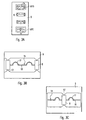
- Fig. 3A shows a schematic representation of a carrier 9, which contains the coupling lines 1 required for a YIG bandpass filter 2 with four YIG elements 6.
- the coupling lines 1 are formed in the embodiment in the form of an input or output line 1a and three connecting lines 1b.
- the former is in Fig. 3A arranged at the bottom of the film carrier 9, the latter above.
- Figs. 3B and 3C show the in Fig. 3A sections of support 9 labeled IIIB and IIIC Fig. 3B one of the three connecting lines 1b is shown while Fig. 3C the input or output line 1a shows.
- the coupling lines 1 are held by the process of etching, cutting, punching or eroding from the film prior to separation in the carrier 9 by webs 12 which are formed on the contact lugs 8.
- the coupling lines 1 are mounted in the base body 3 according to their shape and fixed in the base body 3 by soldering, welding or another method of maintaining the electrical conductivity.
Landscapes
- Control Of Motors That Do Not Use Commutators (AREA)
- Inductance-Capacitance Distribution Constants And Capacitance-Resistance Oscillators (AREA)
Abstract
Description
- Die Erfindung betrifft ein YIG-Filter oder ein YIG-Oszillator.
- YIG-Bandpaßfilter oder YIG-Oszillatoren verfügen über zumindest einen Resonator, welcher vorzugsweise kugelförmig ausgebildet und aus einem Yttrium-Eisen-Granat (Yttrium-Iron-Garnet YIG) hergestellt ist. Die Resonatorwirkung wird mittels Kopplungsleitungen vermittelt, die so ausgebildet und angeordnet sein müssen, daß der Mittelpunkt des Resonators und der Mittelpunkt des Biegeradius einer Kopplungsleitung genau übereinstimmen.
- Ein YIG-Bandpaßfilter mit entsprechend ausgebildeten Kopplungsleitungen ist beispielsweise aus der Druckschrift
US 4,480,238 bekannt. Der durchstimmbare YIG-Bandpaßfilter weist dabei einen Grundkörper auf, welcher Schlitze zur Aufnahme von isolierten Plättchen, die an einer Kante eine leitfähige Beschichtung aufweisen, die als Kopplungsleitungen dient, umfaßt. Weiterhin sind Filterkammern zur Aufnahme der YIG-Elemente vorgesehen. Die Plättchen werden so über die YIG-Elemente in die Schlitze eingelegt, daß die YIG-Elemente in Einbuchtungen in den mit der leitfähigen Beschichtung versehenen Kanten angeordnet sind. Die YIG-Elemente und die Plättchen werden in festen Positionen fixiert. - Nachteilig an dem aus der oben genannten Druckschrift bekannten YIG-Bandpaßfilter ist insbesondere die aufwendige Herstellung der die Kopplungsleitungen bildenden Plättchen. Der als Träger dienende Isolator muß zunächst entsprechend geformt und dann mit der leitfähigen Beschichtung versehen werden. Dies ist aufwendig und ausschußgefährdet, da die Beschichtung durch die geringe Schichtdicke empfindlich gegen Beschädigungen ist.
- Aufgabe der vorliegenden Erfindung ist es, ein YIG-Filter oder YIG-Oszillator zu schaffen, mit Kopplungsleitungen die einfach herstellbar, unempfindlich gegen Beschädigungen und leicht einbaubar sind.
- Die Aufgabe wird bezüglich der Kopplungsleitungen durch die kennzeichnenden Merkmale des Anspruchs 1 gelöst.
- Vorteilhafte Weiterbildungen der erfindungsgemäßen Anordnungen sind in den Unteransprüchen angegeben.
-
FR 2 616 972 Abbildung 2 , offenbart eine YIG-Anordnung gemäss dem Oberbegriff des Anspruchs 1. - Im Folgenden werden anhand der Zeichnung bevorzugte Ausführungsbeispiele der Erfindung beispielhaft dargestellt und in der nachfolgenden Beschreibung näher erläutert. Es zeigen:
- Fig. 1A
- eine schematische, perspektivische Darstellung eines bevorzugten Ausführungsbeispiels eines Grundkörpers eines YIG-Handpaßfilters mit Resonatoren und Kopplungeleitungen,
- Fig. 1B
- eine schematische, perspektivische Darstellung der Resonatoren und Kopplungsleitungen ohne Grundkörper,
- Fig. 2A
- eine schematische Darstellung einer beispielhaften Kopplungsleitung für zwei Resonatoren gemäß dem Stand der Technik,
- Fig. 2B
- eine schematische Darstellung eines Ausführungsbeispiels einer erfindungsgemäß ausgestalteten Kopplungsleitung für zwei Resonatoren, und
- Fig.
- 3A-C schematische Darstellungen von erfindungsgemäß ausgestalteten Kopplungsleitungen während des Herstellungsprozesses vor dem Vereinzeln.
-
Fig. 1A zeigt in einer schematischen, perspektivischen Ansicht ein Ausführungsbeispiel eines YIG-Bandpaßfilters 2, der einen Grundkörper 3 und im Ausführungsbeispiel vier in dem Grundkörper 3 ausgebildete Filterkammern 4 mit ebenso vielen YIG-Elementen 6 aufweist. - Die YIG-Elemente 6 sind dabei kugelförmig aus einem Yttrium-Eisen-Granat ausgebildet, auf Haltern 10 beispielsweise durch Kleben mit Epoxydharz montiert und durch Kopplungsleitungen 1 elektromagnetisch gekoppelt.
- Die Filterkammern 4 sind durch Schlitze 5 miteinander verbunden, in welche die Kopplungsleitungen 1 eingelegt sind. Dabei sind im Ausführungsbeispiel jeweils zwei der Filterkammern 4 gleich ausgebildet. In die mit 4a bezeichneten Filterkammern 4 münden Koaxialkabel 11 ein, über die der Signalein- bzw. -auslauf erfolgt. Die mit 4b bezeichneten Filterkammern 4 weisen dagegen nur die YIG-Elemente 6 auf. Die Anzahl der Filterkammern 4b ist dabei nicht auf zwei beschränkt, sondern kann auch eins oder mehr betragen so daß die Gesamtzahl der Filterkammern 4 drei oder mehr betragen kann.
-
Fig. 1B zeigt zur besseren Verständlichkeit die Anordnung der Kopplungsleitungen 1 sowie der auf ihren Haltern 10 montierten YIG-Elemente 6 ohne den umgebenden Grundkörper 3. - Die Kopplungsleitungen 1 sind im Ausführungsbeispiel in zwei verschiedenen Formen ausgeführt. Die die Filterkammern 4b untereinander verbindende Kopplungsleitung 1 ist als Ein- bzw. Ausgangsleitung 1a ausgeführt, während die im Ausführungsbeispiel drei weiteren Kopplungsleitungen 1 als Verbindungsleitungen 1b ausgeführt sind.
- Wie aus
Fig. 1B hervorgeht, weisen die Kopplungsleitungen 1 Kontaktfahnen 8 auf, welche einerseits der Masseverbindung der Kopplungsleitungen 1 im Grundkörper 3 und andererseits der Fixierung der Kopplungsleitungen 1 in den Schlitzen 5 dienen. Die Kontaktfahnen 8 sind dabei rechteckig geformt, wobei eine Kantenlänge der Kontaktfahnen 8 ungefähr der axialen Dicke des Grundkörpers 2 entspricht. - Betrachtet man die
Fig. 2A und 2B , ist erkennbar, wodurch sich die Kopplungsleitungen 1 gemäßFig. 2B von herkömmlichen Kopplungsleitungen 1 gemäßFig. 2A unterscheiden. - Den beiden Ausführungsformen ist gemeinsam, daß jeweils zumindest ein gekrümmter Abschnitt 17 vorgesehen ist, der jeweils ein YIG-Element 6 so zumindest teilweise umgreift, daß ein Mittelpunkt des YIG-Elements 6 mit einem Mittelpunkt des gekrümmten Abschnitts 17 zusammenfällt. Weiterhin ist zumindest ein Leitungsabschnitt 18 vorgesehen.
- Die in
Fig. 2A dargestellte Kopplungsleitung 1 gemäß dem Stand der Technik ist aus einem Draht gebogen. Hierbei werden zunächst die YIG-Elemente 6 in den inFig. 2A und 2B nicht näher dargestellten Grundkörper 3 eingebracht und dann der nur grob vorgebogene Draht in die Schlitze 5 eingelegt. Eine Messung des Koppelungsgrades ergibt dann, wo die Kopplungsleitung 1 noch nachgebogen werden muß. Dies erfolgt händisch mittels eines geeigneten Werkzeugs. Danach muß erneut kontrolliert und u.U. wieder nachjustiert werden. Zu diesem Zweck muß jedes Mal der YIG-Filter 2 oder YIG-Oszillator geöffnet und anschließend zum Vornehmen der Messung wieder zusammengebaut werden. Das Verfahren ist somit äußerst aufwendig und führt oftmals sogar dazu, daß das Werkstück nach mehreren Iterationen vollkommen verworfen werden muß, weil keine befriedigende Kopplung erreicht wird. - Demgegenüber werden die erfindungsgemäß ausgestalteten Kopplungsleitungen 1 gemäß
Fig. 2B aus einer metallischen Folie durch geeignete Verfahren wie Ätzen, Erodieren, Schneiden, insbesondere Laserschneiden oder Wasserstrahlschneiden und/oder Stanzen hergestellt und montiert. Danach erfolgt die korrekte Positionierung der YIG-Elemente 6 relativ zu den Kopplungsleitungen 1. - Die Folie besteht aus einer Kupfer-Beryllium-Legierung, um sowohl den Anforderungen an die Elastizität als auch an die Festigkeit zu genügen. Die Dicke der Folie beträgt dabei vorzugsweise ca. 50 µm.
- Die Herstellung der Kopplungsleitungen 1 aus der Folie erfolgt in mehreren Bearbeitungsschritten. Zunächst wird die Folie gereinigt und auf beiden Seiten mit einem Positivlack bei einer Justiergenauigkeit von ca. 5 µm in einer Schichtdicke von ca. 5 µm aufgetragen, um eine Maske zu erstellen. Danach erfolgt die Herstellung der Kopplungsleitungen 1 beispielsweise durch Sprühätzen mit Eisenchlorid. (FeCl3) Anschließend werden die in Form eines Trägers 9 mit einer vorher festgelegten Anzahl von Kopplungsleitungen 1 von Lackresten befreit und galvanisch mit einer Goldbeschichtung von ca. 5 µm versehen. Danach folgt ein Härtungsvorgang für beispielsweise eine Stunde bei 325°C. Dann können die Kopplungsleitungen aus dem Folien-Träger 9 gelöst und verbaut werden.
- Die Kopplungsleitungen 1 weisen durch das beschriebene Herstellungsverfahren eine feste Form mit einem genau definierten Krümmungsradius in den gekrümmten Abschnitten 17 bei einer gleichmäßigen Krümmung auf. Die YIG-Elemente 6 werden dann relativ zu den Kopplungsleitungen 1 ausgerichtet. Dies ist gegenüber dem Stand der Technik einfacher und mit erheblich geringerem Aufwand verbunden, weil die Herstellungsgenauigkeit bei den erfindungsgemäß ausgestalteten Kopplungsleitungen 1 erheblich größer ist als bei händisch gebogenen Kopplungsleitungen 1.
-
Fig. 3A zeigt in einer schematischen Darstellung einen Träger 9, welcher die für einen YIG-Bandpaßfilter 2 mit vier YIG-Elementen 6 benötigten Kopplungsleitungen 1 enthält. - Wie bereits weiter oben erwähnt, sind die Kopplungsleitungen 1 im Ausführungsbeispiel in Form einer Ein- bzw. Ausgangsleitung 1a sowie dreier Verbindungsleitungen 1b ausgebildet. Die erstere ist in
Fig. 3A ganz unten in dem Folien-Träger 9 angeordnet, die letzteren darüber. - Die
Fig. 3B und 3C zeigen die inFig. 3A mit IIIB und IIIC bezeichneten Ausschnitte aus dem Träger 9. InFig. 3B ist eine der drei Verbindungsleitungen 1b dargestellt, währendFig. 3C die Ein- bzw. Ausgangsleitung 1a zeigt. - Aus den
Fig. 3B und 3C ist erkennbar, daß die Kopplungsleitungen 1 nach dem Vorgang des Ätzens, Schneidens, Stanzens oder Erodierens aus der Folie vor dem Vereinzeln in dem Träger 9 durch Stege 12 gehalten werden, die an den Kontaktfahnen 8 ausgebildet sind. Beim Vereinzeln der Kopplungsleitungen 1 werden die Kopplungsleitungen 1 aus dem Träger 9 durch Brechen der Stege 12 separiert. Nach dem Vereinzeln werden die Kopplungsleitungen 1 entsprechend ihrer Form in dem Grundkörper 3 montiert und durch Löten, Schweißen oder ein anderes, die elektrische Leitfähigkeit erhaltendes Verbindungsverfahren in dem Grundkörper 3 fixiert.
Claims (6)
- YIG-Filter (2) oder YIG-Oszillator, umfassend einen Grundkörper (3) in dem Filterkammern (4) ausgebildet sind, wobei jede Filterkammer (4) ein YIG-Element (6) aufweist und die Filterkammern (4) durch Schlitze (5) im Grundkörper (3) die über die Filterkammern hinausreichen, miteinander verbunden sind, wobei eine Kopplungsleitung (1), zur elektromagnetischen Kopplung der YIG-Elemente (6), zumindest einen gekrümmten Abschnitt (17), der ein YIG-Element (6) zumindest teilweise umgreift, und zumindest einen, in einem Schlitz (5) eingelegten Leitungsabschnitt (18) aufweist, wobei die Kopplungsleitung (1) mit dem Leitungsabschnitt (18) elektrisch Leitfähig in den Schlitzen (5) fixiert ist, dadurch gekennzeichnet, dass der Leitungsabschnitt (18) der Kopplungsleitung (1) zumindest eine einstückig mit ihr ausgebildete Kontaktfahne (8) aufweist , wobei eine Kantenlänge der Kontaktfahne (8) ungefähr der axialen Dicke des Grundkörpers (3) entspricht, und die Fixierung der Kopplungsleitung (1) mittels der Kontaktfahnen (8) realisiert ist.
- YIJG-Filter (2) oder YIG-Oszillator
nach Anspruch 1,
dadurch gekennzeichnet,
dass die zumindest eine Kontaktfahne (8) rechteckig geformt ist. - YIG-Filter (2) oder YIG-Oszillator nach einem der Ansprüche 1 oder 2,
dadurch gekennzeichnet,
dass die Kopplungsleitung (1) als Ein- bzw. Ausgangsleitung (1a) oder als Verbindungsleitung (1b) ausgebildet ist. - YIG-Filter (2) oder YIG-Oszillator nach Anspruch 1,
dadurch gekennzeichnet,
dass die Kopplungsleitung (1) eine metallische Folie aus einer Legierung aus Kupfer und Beryllium ist. - YIG-Filter (2) oder YIG-Oszillator nach Anspruch 4,
dadurch gekennzeichnet,
dass die Dicke der Folie 10 bis 100 µm, besonders bevorzugt 25 bis 75 µm, besonders bevorzugt etwa 50 µm beträgt. - YIG-Filter (2) oder YIG-Oszillator nach einem der Ansprüche 1 bis 5,
dadurch gekennzeichnet,
dass der zumindest eine gekrümmte Abschnitt (17) der Kopplungsleitung (1) einen Krümmungsradius aufweist.
Applications Claiming Priority (2)
| Application Number | Priority Date | Filing Date | Title |
|---|---|---|---|
| DE102004056259A DE102004056259A1 (de) | 2004-11-22 | 2004-11-22 | Kopplungsleitungen für einen YIG-Filter oder YIG-Oszillator und Verfahren zur Herstellung der Kopplungsleitungen |
| PCT/EP2005/011885 WO2006056314A1 (de) | 2004-11-22 | 2005-11-07 | Kopplungsleitungen für einen yig-filter oder yig-oszillator und verfahren zur herstellung der kopplungsleitungen |
Publications (3)
| Publication Number | Publication Date |
|---|---|
| EP1815554A1 EP1815554A1 (de) | 2007-08-08 |
| EP1815554B1 true EP1815554B1 (de) | 2010-10-27 |
| EP1815554B8 EP1815554B8 (de) | 2011-01-19 |
Family
ID=35735322
Family Applications (1)
| Application Number | Title | Priority Date | Filing Date |
|---|---|---|---|
| EP05813554A Expired - Lifetime EP1815554B8 (de) | 2004-11-22 | 2005-11-07 | Kopplungsleitungen für einen yig-filter oder yig-oszillator und verfahren zur herstellung der kopplungsleitungen |
Country Status (5)
| Country | Link |
|---|---|
| US (2) | US7573357B2 (de) |
| EP (1) | EP1815554B8 (de) |
| JP (1) | JP4589402B2 (de) |
| DE (2) | DE102004056259A1 (de) |
| WO (1) | WO2006056314A1 (de) |
Families Citing this family (3)
| Publication number | Priority date | Publication date | Assignee | Title |
|---|---|---|---|---|
| US11923590B2 (en) * | 2018-10-29 | 2024-03-05 | Universitaet Hamburg | Magnetically tunable resonator |
| TR201907601A2 (tr) * | 2019-05-20 | 2020-12-21 | Aselsan Elektronik Sanayi Ve Ticaret As | YIG Filtrelerinde Oluşan Merkez Frekans Kaymasını ve Doğrusallık Hatalarını Minimize Eden Yöntem |
| CN110165344B (zh) * | 2019-05-28 | 2021-08-27 | 西南应用磁学研究所 | 旋磁滤波器谐振电路结构 |
Citations (1)
| Publication number | Priority date | Publication date | Assignee | Title |
|---|---|---|---|---|
| FR2616972A1 (fr) * | 1987-06-22 | 1988-12-23 | Enertec | Filtre passe-bande a bille de grenat d'yttrium fer accordable en frequence et a large bande d'accord |
Family Cites Families (18)
| Publication number | Priority date | Publication date | Assignee | Title |
|---|---|---|---|---|
| NL158239B (nl) * | 1950-12-29 | Polensky & Zoellner | Voortschuifsteigerwerk. | |
| US3821668A (en) * | 1973-03-12 | 1974-06-28 | Loral Corp | Electronically tunable microwave filter |
| JPS5850701U (ja) * | 1981-09-18 | 1983-04-06 | 株式会社アドバンテスト | マイクロ波バンドパスフイルタ |
| US4633205A (en) * | 1985-11-25 | 1986-12-30 | Tektronix, Inc. | Loop coupled YIG resonator |
| US4857871A (en) * | 1988-10-31 | 1989-08-15 | Harris David L | Magnetic field-tunable filter with plural section housing and method of making the same |
| JPH0429204U (de) * | 1990-07-02 | 1992-03-09 | ||
| US5294899A (en) * | 1992-07-29 | 1994-03-15 | Hewlett-Packard Company | YIG-tuned circuit with rotatable magnetic polepiece |
| US5580466A (en) * | 1993-04-14 | 1996-12-03 | Hitachi Construction Machinery Co., Ltd. | Metal plate processing method, lead frame processing method, lead frame, semiconductor device manufacturing method, and semiconductor device |
| US5757125A (en) * | 1995-11-09 | 1998-05-26 | Astronics Corporation, Inc. | Electroluminescent lamp with lead attachment isolation structure, and rotary abrasion method of manufacture thereof |
| US5959513A (en) * | 1997-05-13 | 1999-09-28 | Verticom, Inc. | Microwave ferrite resonator mounting structure having reduced mechanical vibration sensitivity |
| JP3622639B2 (ja) * | 2000-05-30 | 2005-02-23 | 株式会社村田製作所 | 非可逆回路素子の製造方法 |
| US6670208B2 (en) * | 2000-06-23 | 2003-12-30 | Nec Corporation | Optical circuit in which fabrication is easy |
| GB2365007B (en) * | 2000-07-21 | 2002-06-26 | Murata Manufacturing Co | Insulative ceramic compact |
| US6772515B2 (en) * | 2000-09-27 | 2004-08-10 | Hitachi, Ltd. | Method of producing multilayer printed wiring board |
| US6727775B2 (en) * | 2001-11-29 | 2004-04-27 | Sirenza Microdevices, Inc. | Ferrite crystal resonator coupling structure |
| DE10212018A1 (de) * | 2002-03-19 | 2003-10-02 | Bosch Gmbh Robert | Isolationsmaterial und Gassensor |
| US7198764B2 (en) * | 2003-03-05 | 2007-04-03 | Delphi Technologies, Inc. | Gas treatment system and a method for using the same |
| US20060035782A1 (en) * | 2004-08-12 | 2006-02-16 | Ford Global Technologies, Llc | PROCESSING METHODS AND FORMULATIONS TO ENHANCE STABILITY OF LEAN-NOx-TRAP CATALYSTS BASED ON ALKALI- AND ALKALINE-EARTH-METAL COMPOUNDS |
-
2004
- 2004-11-22 DE DE102004056259A patent/DE102004056259A1/de not_active Withdrawn
-
2005
- 2005-11-07 JP JP2007541743A patent/JP4589402B2/ja not_active Expired - Lifetime
- 2005-11-07 WO PCT/EP2005/011885 patent/WO2006056314A1/de not_active Ceased
- 2005-11-07 DE DE502005010453T patent/DE502005010453D1/de not_active Expired - Lifetime
- 2005-11-07 EP EP05813554A patent/EP1815554B8/de not_active Expired - Lifetime
- 2005-11-07 US US11/667,897 patent/US7573357B2/en not_active Expired - Lifetime
-
2009
- 2009-02-11 US US12/369,498 patent/US8327520B2/en active Active
Patent Citations (1)
| Publication number | Priority date | Publication date | Assignee | Title |
|---|---|---|---|---|
| FR2616972A1 (fr) * | 1987-06-22 | 1988-12-23 | Enertec | Filtre passe-bande a bille de grenat d'yttrium fer accordable en frequence et a large bande d'accord |
Also Published As
| Publication number | Publication date |
|---|---|
| WO2006056314A1 (de) | 2006-06-01 |
| EP1815554A1 (de) | 2007-08-08 |
| US20090144964A1 (en) | 2009-06-11 |
| JP4589402B2 (ja) | 2010-12-01 |
| US20080211605A1 (en) | 2008-09-04 |
| DE502005010453D1 (de) | 2010-12-09 |
| US7573357B2 (en) | 2009-08-11 |
| JP2008521299A (ja) | 2008-06-19 |
| EP1815554B8 (de) | 2011-01-19 |
| DE102004056259A1 (de) | 2006-05-24 |
| US8327520B2 (en) | 2012-12-11 |
Similar Documents
| Publication | Publication Date | Title |
|---|---|---|
| DE10207342A1 (de) | Verfahren zum Liefern unterschiedlicher Frequenzeinstellungen bei einem akustischen Dünnfilmvolumenresonator- (FBAR-) Filter und Vorrichtung, die das Verfahren beinhaltet | |
| DE10207341A1 (de) | Verfahren zum Erzeugen akustischer Dünnfilmvolumenresonatoren (FBARs) mit unterschiedlichen Frequenzen auf einem einzelnen Substrat und Vorrichtung, die das Verfahren beinhaltet | |
| EP3593412B1 (de) | Innenleiter-element und verfahren zum herstellen eines systems | |
| EP1128476B2 (de) | Verfahren zur Herstellung eines Steckverbinders | |
| WO2013083257A1 (de) | Verfahren zum herstellen eines steckverbinders | |
| EP1815554B1 (de) | Kopplungsleitungen f]r einen yig-filter oder yig-oszillator und verfahren zur herstellung der kopplungsleitungen | |
| DE4310369A1 (de) | Adapter | |
| WO2005053103A1 (de) | Koaxialkabel und verfahren zu dessen herstellung | |
| EP1741162B1 (de) | Elektrische funktionseinheit und verfahren zu deren herstellung | |
| EP0811995B1 (de) | Magnetspule sowie Verfahren zu deren Herstellung | |
| DE69614983T2 (de) | Piezoelektrischer Resonator | |
| EP1318565B1 (de) | Antenne, insbesondere Mobilfunkantenne, mit einer Zentrierhilfe bei ihrer Herstellung | |
| EP1771915B1 (de) | Grundkörper für einen yig-filter oder yig-oszillator | |
| DE102016200243A1 (de) | Kontaktverbinder, Anschlusskontakt und Verfahren zur Herstellung eines Kontaktverbinders | |
| DE3408581A1 (de) | Resonator | |
| EP1774543B1 (de) | Elektrisches bauelement und verfahren zur herstellung eines elektrischen bauelements | |
| EP3465841B1 (de) | Koaxialsteckverbinder | |
| DE10045073A1 (de) | Steckerelement und zugehöriges Herstellungsverfahren | |
| DE3200117C2 (de) | Einbau-Bandpaßfilteranordnung für ein Koaxialkabel | |
| DE4130390C2 (de) | Widerstandselement | |
| EP0957529A1 (de) | Verfahren zum Abgleichen der Resonanzfrequenz eines Ringresonators | |
| DE19526583A1 (de) | Dielektrisches Filter | |
| DE2905677A1 (de) | Hohlraum-resonator | |
| EP3133696A1 (de) | Kontaktierungsvorrichtung und verfahren zur herstellung | |
| DE102024127800B3 (de) | Verfahren zum zumindest teil- oder bereichsweisen elektrischen isolieren einer erdungs- und/oder kurzschließvorrichtung |
Legal Events
| Date | Code | Title | Description |
|---|---|---|---|
| PUAI | Public reference made under article 153(3) epc to a published international application that has entered the european phase |
Free format text: ORIGINAL CODE: 0009012 |
|
| 17P | Request for examination filed |
Effective date: 20070404 |
|
| AK | Designated contracting states |
Kind code of ref document: A1 Designated state(s): DE FR GB |
|
| DAX | Request for extension of the european patent (deleted) | ||
| 17Q | First examination report despatched |
Effective date: 20070914 |
|
| RBV | Designated contracting states (corrected) |
Designated state(s): DE FR GB |
|
| GRAP | Despatch of communication of intention to grant a patent |
Free format text: ORIGINAL CODE: EPIDOSNIGR1 |
|
| GRAS | Grant fee paid |
Free format text: ORIGINAL CODE: EPIDOSNIGR3 |
|
| GRAA | (expected) grant |
Free format text: ORIGINAL CODE: 0009210 |
|
| AK | Designated contracting states |
Kind code of ref document: B1 Designated state(s): DE FR GB |
|
| REG | Reference to a national code |
Ref country code: GB Ref legal event code: FG4D Free format text: NOT ENGLISH |
|
| REF | Corresponds to: |
Ref document number: 502005010453 Country of ref document: DE Date of ref document: 20101209 Kind code of ref document: P |
|
| PLBE | No opposition filed within time limit |
Free format text: ORIGINAL CODE: 0009261 |
|
| STAA | Information on the status of an ep patent application or granted ep patent |
Free format text: STATUS: NO OPPOSITION FILED WITHIN TIME LIMIT |
|
| 26N | No opposition filed |
Effective date: 20110728 |
|
| REG | Reference to a national code |
Ref country code: DE Ref legal event code: R097 Ref document number: 502005010453 Country of ref document: DE Effective date: 20110728 |
|
| REG | Reference to a national code |
Ref country code: FR Ref legal event code: PLFP Year of fee payment: 11 |
|
| REG | Reference to a national code |
Ref country code: FR Ref legal event code: PLFP Year of fee payment: 12 |
|
| REG | Reference to a national code |
Ref country code: FR Ref legal event code: PLFP Year of fee payment: 13 |
|
| P01 | Opt-out of the competence of the unified patent court (upc) registered |
Effective date: 20230525 |
|
| PGFP | Annual fee paid to national office [announced via postgrant information from national office to epo] |
Ref country code: DE Payment date: 20241119 Year of fee payment: 20 |
|
| PGFP | Annual fee paid to national office [announced via postgrant information from national office to epo] |
Ref country code: GB Payment date: 20241121 Year of fee payment: 20 |
|
| PGFP | Annual fee paid to national office [announced via postgrant information from national office to epo] |
Ref country code: FR Payment date: 20241120 Year of fee payment: 20 |
|
| REG | Reference to a national code |
Ref country code: DE Ref legal event code: R071 Ref document number: 502005010453 Country of ref document: DE |
|
| REG | Reference to a national code |
Ref country code: GB Ref legal event code: PE20 Expiry date: 20251106 |