EP1811311B1 - Dispositif pour mesurer le courant - Google Patents
Dispositif pour mesurer le courant Download PDFInfo
- Publication number
- EP1811311B1 EP1811311B1 EP07100349.5A EP07100349A EP1811311B1 EP 1811311 B1 EP1811311 B1 EP 1811311B1 EP 07100349 A EP07100349 A EP 07100349A EP 1811311 B1 EP1811311 B1 EP 1811311B1
- Authority
- EP
- European Patent Office
- Prior art keywords
- magnetic field
- yoke
- air gap
- current
- field sensor
- Prior art date
- Legal status (The legal status is an assumption and is not a legal conclusion. Google has not performed a legal analysis and makes no representation as to the accuracy of the status listed.)
- Active
Links
- 230000005291 magnetic effect Effects 0.000 claims description 142
- 239000004020 conductor Substances 0.000 claims description 36
- 239000004065 semiconductor Substances 0.000 claims description 16
- 230000005294 ferromagnetic effect Effects 0.000 claims description 15
- 230000035699 permeability Effects 0.000 claims description 10
- 239000002184 metal Substances 0.000 claims description 6
- 229910052751 metal Inorganic materials 0.000 claims description 6
- 239000000696 magnetic material Substances 0.000 claims description 4
- 238000005452 bending Methods 0.000 claims description 2
- 150000002739 metals Chemical class 0.000 claims 1
- 238000005259 measurement Methods 0.000 description 22
- 230000003321 amplification Effects 0.000 description 17
- 238000003199 nucleic acid amplification method Methods 0.000 description 17
- 230000000694 effects Effects 0.000 description 4
- 230000007423 decrease Effects 0.000 description 3
- 239000000463 material Substances 0.000 description 3
- XEEYBQQBJWHFJM-UHFFFAOYSA-N Iron Chemical compound [Fe] XEEYBQQBJWHFJM-UHFFFAOYSA-N 0.000 description 2
- 238000010276 construction Methods 0.000 description 2
- 230000001419 dependent effect Effects 0.000 description 2
- 238000011156 evaluation Methods 0.000 description 2
- 102000003712 Complement factor B Human genes 0.000 description 1
- 108090000056 Complement factor B Proteins 0.000 description 1
- 230000003247 decreasing effect Effects 0.000 description 1
- 238000011161 development Methods 0.000 description 1
- 230000018109 developmental process Effects 0.000 description 1
- 238000009434 installation Methods 0.000 description 1
- 229910052742 iron Inorganic materials 0.000 description 1
- 230000002787 reinforcement Effects 0.000 description 1
- 125000006850 spacer group Chemical group 0.000 description 1
- 210000002105 tongue Anatomy 0.000 description 1
Images


Classifications
-
- G—PHYSICS
- G01—MEASURING; TESTING
- G01R—MEASURING ELECTRIC VARIABLES; MEASURING MAGNETIC VARIABLES
- G01R15/00—Details of measuring arrangements of the types provided for in groups G01R17/00 - G01R29/00, G01R33/00 - G01R33/26 or G01R35/00
- G01R15/14—Adaptations providing voltage or current isolation, e.g. for high-voltage or high-current networks
- G01R15/20—Adaptations providing voltage or current isolation, e.g. for high-voltage or high-current networks using galvano-magnetic devices, e.g. Hall-effect devices, i.e. measuring a magnetic field via the interaction between a current and a magnetic field, e.g. magneto resistive or Hall effect devices
- G01R15/207—Constructional details independent of the type of device used
-
- G—PHYSICS
- G01—MEASURING; TESTING
- G01R—MEASURING ELECTRIC VARIABLES; MEASURING MAGNETIC VARIABLES
- G01R15/00—Details of measuring arrangements of the types provided for in groups G01R17/00 - G01R29/00, G01R33/00 - G01R33/26 or G01R35/00
- G01R15/14—Adaptations providing voltage or current isolation, e.g. for high-voltage or high-current networks
- G01R15/18—Adaptations providing voltage or current isolation, e.g. for high-voltage or high-current networks using inductive devices, e.g. transformers
- G01R15/183—Adaptations providing voltage or current isolation, e.g. for high-voltage or high-current networks using inductive devices, e.g. transformers using transformers with a magnetic core
- G01R15/185—Adaptations providing voltage or current isolation, e.g. for high-voltage or high-current networks using inductive devices, e.g. transformers using transformers with a magnetic core with compensation or feedback windings or interacting coils, e.g. 0-flux sensors
-
- G—PHYSICS
- G01—MEASURING; TESTING
- G01R—MEASURING ELECTRIC VARIABLES; MEASURING MAGNETIC VARIABLES
- G01R15/00—Details of measuring arrangements of the types provided for in groups G01R17/00 - G01R29/00, G01R33/00 - G01R33/26 or G01R35/00
- G01R15/14—Adaptations providing voltage or current isolation, e.g. for high-voltage or high-current networks
- G01R15/20—Adaptations providing voltage or current isolation, e.g. for high-voltage or high-current networks using galvano-magnetic devices, e.g. Hall-effect devices, i.e. measuring a magnetic field via the interaction between a current and a magnetic field, e.g. magneto resistive or Hall effect devices
- G01R15/202—Adaptations providing voltage or current isolation, e.g. for high-voltage or high-current networks using galvano-magnetic devices, e.g. Hall-effect devices, i.e. measuring a magnetic field via the interaction between a current and a magnetic field, e.g. magneto resistive or Hall effect devices using Hall-effect devices
Definitions
- the invention relates to a device for current measurement referred to in the preamble of claim 1 Art.
- Such a device for measuring current can also be referred to as a current sensor, in particular if it can be sold commercially as a single-part product.
- a current sensor is known from the EP 772046 ,
- the current sensor consists of a current conductor, a magnetic field sensor for measuring the magnetic field generated by a current flowing through the current conductor, and a ferromagnetic yoke.
- the magnetic field sensor comprises a semiconductor chip with two magnetic field concentrators arranged on the surface of the semiconductor chip, which are separated by an air gap, and two horizontal Hall elements integrated in the semiconductor chip, which are arranged on both sides of the air gap, so that they are flooded by field lines of the magnetic field which are from the first Magnetic field concentrator near the air gap go away and impinge on the second magnetic field concentrator near the air gap.
- the semiconductor chip also contains the necessary for the operation of the Hall elements and the amplification and evaluation of the voltage signals supplied by the Hall elements electronic circuits.
- the magnetic field sensor is arranged on the current conductor, so that the magnetic field lines generated by the current are approximately parallel to the surface of the semiconductor chip and thus also parallel to the magnetic field concentrators.
- the yoke surrounds the conductor on three sides and forms an approximately closed magnetic circuit with the two magnetic field concentrators.
- the yoke and the two magnetic field concentrators form a magnetic amplifier that amplifies the magnetic field generated by the current. Disadvantages of this current sensor are that it is due to its construction as a current sensor with integrated conductor only for the measurement of relatively small currents of up to 20A suitable and that external magnetic interference fields are hardly shielded.
- the invention has for its object to develop a device for current measurement, which in a simple manner for the measurement of currents in a relatively small measuring range of 0 to typically 20A or 50A or 100A, as well as for the measurement of currents in a relatively large Measuring range from 0 to 200A or 300A can be designed, which is briefly overloaded with an overload current of up to 1000A and which is well shielded against external magnetic interference fields.
- the current measuring device comprises a magnetic field sensor for measuring the magnetic field generated by a current flowing through a current conductor, and a yoke made of a high permeability magnetic material surrounding the current conductor in the measuring region.
- the yoke consists in principle of an elongated piece of sheet metal with two ends, which has been brought by bending in a mold in which the end faces of the sheet are opposite to each other and separated by an air gap.
- the yoke is therefore like a piece of pipe with a slot running in the pipe direction.
- the yoke completely encloses the conductor except for the air gap.
- the magnetic field sensor is preferably a magnetic field sensor with a Hall element integrated in a semiconductor chip and an electronic circuit integrated in the semiconductor chip for operating the Hall element and with two magnetic field concentrators arranged on the active top side of the semiconductor chip and separated by an air gap, the Hall element being field lines of the magnetic field flooded, which go away from the first magnetic field concentrator in the vicinity of the air gap and impinge on the second magnetic field concentrator in the vicinity of the air gap.
- the magnetic field sensor can also be another sensor, z.
- the yoke serves on the one hand to amplify the magnetic field generated by the current and on the other hand to shield external magnetic interference fields.
- the magnetic field sensor and the yoke are matched to each other such that the magnetic field sensor is only sensitive to a single component of the magnetic field, which is referred to as x-component example, and that the yoke shields exactly this x-component.
- the magnetic field sensor therefore measures only the x-component of the magnetic field generated by the current flowing in the current conductor, but not the shielded x-component of an external magnetic interference field.
- the ends of the yoke are tapered so that a width of the ends of the yoke is less than a width of the yoke.
- the extent of the yoke in the direction to be shielded (that is, in the x direction) is at least as large as a height measured perpendicular thereto.
- the shield can be further increased by an additional, substantially U-shaped, the yoke enclosing three sides screen.
- the ratio of shielding factor to gain factor can also be increased by either widening the ends of the yoke and / or providing it with a recess.
- Such a configuration of the yoke is also suitable for the measurement of currents in a comparatively large range of 0 to 200A or 300A, but also 1000A.
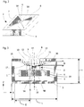
- the Fig. 1 and Fig. 3 show in perspective view and cross section a device for measuring the current flowing through a conductor 1 electrical current I, which is designed according to the invention for the measurement of a current in the range of 0 to typically 20A or 50A, in the maximum of about 100A.
- the cross section of the conductor 1 is preferably rectangular.
- the coordinates of a Cartesian coordinate system are denoted by x, y and z.
- the current flows in the y-direction.
- the current measuring device comprises a magnetic field sensor 2 which measures the magnetic field generated by the current I and a yoke 3 made of a material of high magnetic permeability.
- high permeability is meant a relative permeability of at least 100 (the relative permeability of air is 1).
- the yoke 3 is formed, for example, from a single sheet of iron or mumetal whose relative permeability is typically in the range between 100 and 100,000.
- the yoke 3 is formed of an elongate piece of sheet metal of about 0.5 to 2 mm thickness with two ends 10 and 11 so that it almost completely encloses the conductor 1, namely so that the two end faces 12 and 13 of the ends 10 and 11 of Sheet metal opposite each other and separated by an air gap 14.
- the current conductor 1 and the magnetic field sensor 2 are thus located completely within the yoke 3.
- the ends 10 and 11 of the yoke 3 are tapered, so that their width B 0 is less than the width B of the sheet or yoke 3.
- the conductor 1 is tapered in the region of the yoke 3.
- FIG Fig. 2 A preferred example of the magnetic field sensor 2 is shown in FIG Fig. 2 It contains a semiconductor chip 4 with at least one Hall element, in the example two Hall elements 5A and 5B, and an electronic circuit for the operation of the at least one Hall element and the evaluation of the Hall voltage supplied by the at least one Hall element.
- a semiconductor chip 4 with at least one Hall element in the example two Hall elements 5A and 5B, and an electronic circuit for the operation of the at least one Hall element and the evaluation of the Hall voltage supplied by the at least one Hall element.
- two magnetic field concentrators 7, 8 separated by an air gap 6 are arranged such that the at least one Hall element of field lines 9 (see FIG Fig. 3 ) of the magnetic field flowing away from the first magnetic field concentrator 7 in the vicinity of the air gap 6 and impinge on the second magnetic field concentrator 8 in the vicinity of the air gap 6.
- the structure of such a magnetic field sensor 2 is made the European patent EP 772046 known.
- the Hall element (or the two Hall elements 5A and 5B) is a so-called horizontal Hall element which is sensitive to a magnetic field which is perpendicular to the active surface of the semiconductor chip 4, in this case in the z direction.
- the term Hall element is not to be understood as a single Hall element, but it may be understood as including a group of parallel or antiparallel connected and / or operated in time division Hall elements. Such arrangements of Hall elements are used to reduce the offset of the Hall voltage.
- the Hall element may also be a so-called vertical Hall element, which is sensitive to a magnetic field which is parallel to the active surface of the semiconductor chip 4 and perpendicular to the current direction, in this case in the x direction.
- the magnetic field sensor 2 is packed in a housing 24.
- the magnetic field sensor 2 is sensitive (in the absence of the yoke 3) to a magnetic field that extends in the x-direction, and insensitive to magnetic fields that extend in the y and z directions.
- the two magnetic field concentrators 7 and 8 extend in the x direction.
- the housing 24 requires more space than the air gap 14 of the yoke 3 is available. The housing 24 is thus located inside the yoke 3, but outside the air gap 14.
- the existing between the end faces 12 and 13 of the ends 10 and 11 of the yoke 3 air gap 14 is "above" the air gap 6 between the two magnetic field concentrators 7 and 8, or, geometrically expressed: There is a perpendicular to the surface of the semiconductor chip 4 extending plane which passes through both the air gap 6 and the air gap 14 therethrough.
- the yoke 3 and the two magnetic field concentrators 7 and 8 thus form a through the air gap 6 and two further air gaps 15, 16 (see Fig. 3 ) broken magnetic circuit, with field lines 17 (see Fig.
- the device for measuring current is designed so that the two magnetic field concentrators 7 and 8 are not directly in the air gap 14 of the yoke 3, but below the air gap 14, where they are flooded mainly by scattering lines of the magnetic field from the ends 10 and 11 of the Yokes 3 go out.
- the distance D of the magnetic field sensor 2, measured from the surface of the magnetic field concentrators 7 and 8, from the air gap 14 of the yoke 3 is smaller than a distance E of the magnetic field sensor 2, measured from the outer end of the magnetic field concentrators 7 and 8, of the Sidewalls of the yoke 3.
- the yoke 3 fulfills two functions, namely on the one hand the magnetic amplification of the magnetic field generated by the current flowing in the current conductor and on the other hand the shielding of the magnetic field sensor against external magnetic interference fields. Due to its construction, the magnetic field sensor 2 is insensitive to external magnetic fields which are directed in the y- and / or z-direction.
- the amplification of the magnetic field generated by the current flowing in the conductor at the location of Hall elements is characterized by a gain factor.
- the amplification factor is dependent on the geometry of the yoke 3, but also on the frequency of the current 1. In the following, the amplification factor usually means the amplification factor for direct current or alternating currents below a certain limit frequency f G.
- the efficiency of the shielding of the magnetic field sensor 2 against an external x-directional magnetic field is characterized by a shielding factor.
- the taper of the ends 10 and 11 to the width B 0 causes an increase in the gain by the factor B / B 0 , while the shielding factor remains almost unchanged.
- the amplification factor and the shielding factor depend on the distance of the magnetic field sensor 2 from the air gap 14 between the ends 10 and 11 of the yoke 3. This situation is based on the Fig. 3 illustrated, which shows the device for measuring current in cross section.
- the conductor 1 and the yoke 3 are rectangular in cross section and arranged symmetrically with respect to a plane of symmetry 18.
- the magnetic field sensor 2 is located on the air gap 14 of the yoke 3 facing side of the conductor 1 and is also placed symmetrically with respect to the plane of symmetry 18 within assembly tolerances, so that the plane of symmetry 18 through the air gap 6 between the two magnetic field concentrators 7 and 8 passes ,
- the magnetic field concentrators 7 and 8 are located at a distance D from the air gap 14 of the yoke 3.
- the amplification factor of the yoke 3 decreases since the proportion of the field lines 17 emanating from the one end 10 of the yoke 3 and the magnetic field concentrator 7 reach, with increasing distance D decreases.
- the shielding factor of the yoke 3 increases with increasing distance D.
- the amplification factor is typically about 10, the shielding factor about 100 to 1000.
- a length L of the yoke 3 measured transversely to the conductor 1 and parallel to the air gap 14 is at least equal to a height H of the yoke 3 measured perpendicular to the air gap 14 Length L at least a factor of 1.5 greater than the height H.
- the Fig. 4 shows a device for current measurement, in which a magnetic field sensor 19 is disposed on the air gap 14 of the yoke 3 facing away from the side of the conductor 1.
- the magnetic field sensor 19 is the same as the magnetic field sensor 2 in the previous example.
- the shielding factor for the magnetic field sensor 19 is also very large here.
- the amplification factor of the yoke 3 for the magnetic field sensor 19 is between 0 and 1, ie, the yoke 3 does not amplify the magnetic field at the location of the second magnetic field sensor 19, but reduces the magnetic field even if the amplification factor is less than one. If the amplification factor is less than 1, this can be exploited to improve the frequency response of the magnetic field sensor 19.
- the output signal of the magnetic field sensor 19 without yoke 3 as a function of the frequency of the current is constant in a frequency range from 0 to f G1 (f G1 is for example 50 kHz) and then typically drops at 20 dB / oct.
- the yoke 3 changes the frequency response, because the amplification factor of the yoke 3 above a cutoff frequency f G2 also decreases.
- the gain factor of yoke 3 for direct currents is already less than 1, then the attenuation of the amplification factor above the cutoff frequency f G2 has a less pronounced effect so that, overall, a lower attenuation occurs above the cutoff frequency f G2 .
- the yoke 3 consists of a single piece of sheet metal.
- the cut-off frequency f G2 of the yoke 3 depends on the thickness d of the sheet: f G 2 ⁇ 1 d
- the thickness d of the sheet is now selected so that f G2 is approximately equal to f G1 .
- the yoke 3 is formed as a laminate of a plurality of sheets separated by an insulating layer of thickness d.
- the thickness d of a sheet is typically about 0.02 to 0.1, at most 0.2 mm.
- the Fig. 5 shows a device for current measurement, in which the magnetic field sensor 2 on the air gap 14 of the yoke 3 facing side of the current conductor 1 and the magnetic field sensor 19 is disposed on the air gap 14 of the yoke 3 facing away from the side of the conductor 1.
- the first magnetic field sensor 2 is used for the accurate measurement of the current in a predetermined operating range of typically 0 to 50A or 0 to 100A, while the second magnetic field sensor 19 for measuring the current above the predetermined working range, in a predetermined overload range from here corresponding to 50A or 100A to typically 1000A.
- the yoke 3 is shown as a laminate of sheets 20 separated by insulating layers.
- the shielding factor may be increased by an additional substantially U-shaped screen 21 of high magnetic permeability material surrounding the yoke 3 on three sides.
- the screen 21 consists of three sections, of which the central section is parallel to the air gap 14 of the yoke 3.
- the screen 21 is preferably made of the same material as the yoke 3.
- the screen 21 is arranged at a distance E to the yoke 3. The distance E is dimensioned so large that the screen 21, the gain of the yoke 3 is not or only slightly reduced.
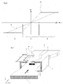
- the Fig. 6 shows the output signals 22 and 23 of the two magnetic field sensors 2 and 19 in function of the current flowing in the current conductor I.
- the output signal 22 of the first magnetic field sensor 2 is proportional to the current I in the predetermined working area A. Above the working area A occur saturation effects of the magnetic field concentrators 7, 8th of the first magnetic field sensor 2, which cause a flattening of the output signal 22.
- the output signal 23 of the second magnetic field sensor 19 is proportional to the current I in the overload region B, since due to the lower amplification factor Saturation effects of the magnetic field concentrators 7, 8 of the second magnetic field sensor 19 only occur at currents above the upper limit of the overload range B.
- the inventive device for current measurement is characterized by a simple, compact design and easy installation.
- the housing 24 with the magnetic field sensor 2 can be glued directly to the conductor 1.
- the housing 24 may be mounted on a circuit board and the circuit board mounted on the conductor 1.
- the yoke 3 can be glued on the opposite side directly or at most via an additional spacer on the conductor 1.
- the magnetic field sensor 2 or 19 should essentially only be sensitive to the x component of an external magnetic field and insensitive to the y and z components of the external magnetic field.
- the magnetic field sensor described above with the two magnetic field concentrators and the Hall element fulfills these requirements to a great extent.
- the magnetic field sensor 2 or 19 may be in all examples, another sensor that meets this requirement, for.
- the magnetic field sensor 2 or 19 can also be a fluxgate sensor.
- a fluxgate sensor comprises a ferromagnetic core.
- the ferromagnetic resistance element or the ferromagnetic core is arranged on the active surface of the semiconductor chip 4.
- the ferromagnetic resistance element or the ferromagnetic core influences the course of the magnetic field lines in a similar manner as the magnetic field concentrators 7, 8 in the previous example.
- the two tapered, opposite ends of the yoke could z. B. also in the form of cut out of the side walls of the yoke punched and bent tongues.
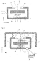
- the Fig. 7 and Fig. 8 show in perspective view two devices for current measurement, which are designed according to the invention for the measurement of currents in a larger range of 0 to 200A or 300A.
- the ends of the yoke 3 are designed so that the magnetic field at the location of the magnetic field sensor 2 is smaller than in a device for current measurement with a yoke 3, whose ends are neither tapered nor broadened, nor provided with a recess, ie have a straight end face with the width B.
- the ends 10 and 11 of the yoke 3 the width B, the end faces 12 and 13 of the yoke 3 but are provided with a recess of width B 1 .
- the ends 10 and 11 of the yoke 3 are widened to the width B 2 . It is also possible a combination, ie a broadening of the ends to the width B 2 > B and the attachment of a recess of width B 1 .
- the amplification factor of the yoke 3 is significantly reduced in this way, while the shielding factor slightly changes. In this way, on the one hand, the ratio of shielding factor to gain factor can be increased and, on the other hand, the amplification factor can be reduced.
- the device for current measurement can be designed solely by changing the shape of the ends of the yoke 3 for the measurement of different sized maximum currents.
- the same magnetic field sensor 2 can be mounted on the current conductor 1 in the same manner and at the same position.
Landscapes
- Physics & Mathematics (AREA)
- General Physics & Mathematics (AREA)
- Measuring Instrument Details And Bridges, And Automatic Balancing Devices (AREA)
Claims (6)
- Dispositif de mesure du courant avec un capteur de champ magnétique (2) renfermée dans un boîtier (24) pour la mesure d'un champ magnétique généré par un courant passant par un conducteur (1) et une culasse (3) en matériau magnétique avec une perméabilité relative d'au moins 100, sachant que le conducteur (1) possède une section carrée, une face inférieure et une face supérieure, sachant que par rapport à un système de coordonnées cartésien avec trois axes désignés axe x, axe y et axe z, le conducteur (1) s'étend dans le sens de l'axe y, dans lequel le courant passe et le capteur de champ magnétique (2) est sensible aux composants du champ magnétique qui s'étend dans le sens de l'axe x, sachant que la culasse (3) est composée par un long morceau de tôle ou un stratifié avec des tôles séparées par des couches d'isolation formé par courbage de telle sorte que la culasse (3) présente deux parois latérales qui s'étendent dans le sens de l'axe z et deux extrémités (10, 11) séparées par un entrefer (14) dont les faces d'extrémité (12, 13) se font face de telle sorte que la culasse (3) enveloppe totalement le conducteur (1) à l'exception de l'entrefer (14), sachant que la culasse présente une longueur (L) mesurée dans le sens de l'axe x et une hauteur (H) mesurée dans le sens d'axe z, le boîtier (24) avec le capteur de champ magnétique (2) est disposé dans la culasse (3) et hors de l'entrefer (14) de la culasse (3) et est collé sur la face supérieure du conducteur (1) ou monté sur un circuit imprimé lui-même fixé sur la face supérieure du conducteur (1), le capteur de champ magnétique (2) comporte au moins un élément à effet Hall (5A; 5B) et deux concentrateurs magnétiques (7, 8) ou est un capteur AMR ou GMR qui englobe un élément de résistance ferromagnétique, ou est un capteur Fluxgate qui englobe un noyau ferromagnétique, sachant que les concentrateurs ferromagnétiques (7, 8) ou l'élément de résistance ferromagnétique ou le noyau ferromagnétique est essentiellement parcouru par des lignes de dispersion du champ magnétique qui partent des extrémités (10, 11) de la culasse (3), la longueur (L) de la culasse (3) est au moins égale à la hauteur (H) de la culasse (3), le capteur de champ magnétique (2) est disposée à une distance (D) de l'entrefer (14) de la culasse (3) mesurée à partir de la surface des concentrateurs magnétiques (7, 8) ou de l'élément de résistance ferromagnétique ou du noyau le long de l'axe z, sachant que la distance (D) est inférieure à la distance la plus courte (E) du capteur de champ magnétique (2) avec les parois latérales de la culasse (3) mesurée à partir de l'extrémité extérieure des concentrateurs magnétiques (7, 8) ou de l'élément de résistance ferromagnétique ou du noyau ferromagnétique le long de l'axe x et la culasse (3) est collée directement ou avec un écarteur sur la face inférieure du conducteur (1).
- Dispositif de mesure du courant selon la revendication 1, caractérisé en ce que les extrémités (10, 11) de la culasse (3) sont diminuées.
- Dispositif de mesure du courant selon la revendication 1, caractérisé en ce que les extrémités (10, 11) de la culasse (3) sont élargies ou pourvues d'une cavité ou élargies et pourvues d'une cavité.
- Dispositif de mesure du courant selon l'une des revendications 1 à 3, caractérisé en ce que sur la face du conducteur (1) opposée à l'entrefer (14) de la culasse (3), un autre capteur de champ magnétique (19) est disposé.
- Dispositif de mesure du courant selon l'une des revendications 1 à 4, caractérisé en ce que le capteur de champ magnétique (2; 19) englobe une puce semi-conductrice (4) avec au moins un élément à effet Hall (5A; 5B), sachant que sur une face supérieure de la puce semi-conductrice (4), sont disposés deux concentrateurs magnétiques (7, 8) séparés par un autre entrefer (6), sachant que l'élément à effet Hall (5A; 5B) est parcouru par des lignes de champ (9) du champ magnétique qui partent du premier concentrateur magnétique (7) à proximité de l'autre entrefer (6) et sortent à proximité de l'autre entrefer (6) sur le deuxième concentrateur magnétique (8).
- Dispositif de mesure du courant selon l'une des revendications 1 à 5 qui comporte également un écran (21) en forme de U enveloppant la culasse (3) par trois côtés en matériau magnétique d'une perméabilité relative d'au moins 100, sachant que l'écran (21) présente trois sections à partir desquelles la section centrale s'étend parallèllement à l'entrefer (14) de la culasse (3).
Applications Claiming Priority (3)
| Application Number | Priority Date | Filing Date | Title |
|---|---|---|---|
| CH962006 | 2006-01-19 | ||
| CH7392006 | 2006-05-08 | ||
| CH9852006 | 2006-06-14 |
Publications (2)
| Publication Number | Publication Date |
|---|---|
| EP1811311A1 EP1811311A1 (fr) | 2007-07-25 |
| EP1811311B1 true EP1811311B1 (fr) | 2016-08-31 |
Family
ID=37963562
Family Applications (1)
| Application Number | Title | Priority Date | Filing Date |
|---|---|---|---|
| EP07100349.5A Active EP1811311B1 (fr) | 2006-01-19 | 2007-01-10 | Dispositif pour mesurer le courant |
Country Status (3)
| Country | Link |
|---|---|
| US (1) | US7545136B2 (fr) |
| EP (1) | EP1811311B1 (fr) |
| JP (1) | JP5787243B2 (fr) |
Cited By (2)
| Publication number | Priority date | Publication date | Assignee | Title |
|---|---|---|---|---|
| DE102021111412A1 (de) | 2021-05-03 | 2022-11-03 | Phoenix Contact Gmbh & Co. Kg | Strommesssystem zur Messung eines durch einen elektrischen Stromleiter fließenden Stroms sowie ein entsprechendes Verfahren |
| LU102798B1 (de) | 2021-05-03 | 2022-11-03 | Phoenix Contact Gmbh & Co | Strommesssystem zur Messung eines durch einen elektrischen Stromleiter fließenden Stroms sowie ein entsprechendes Verfahren |
Families Citing this family (48)
| Publication number | Priority date | Publication date | Assignee | Title |
|---|---|---|---|---|
| EP1811311B1 (fr) | 2006-01-19 | 2016-08-31 | Melexis Technologies NV | Dispositif pour mesurer le courant |
| DE102007003830B4 (de) * | 2007-01-25 | 2009-08-06 | Robert Seuffer Gmbh & Co. Kg | Vorrichtung zur Messung eines durch einen elektrischen Leiter fließenden elektrischen Stroms |
| DE102007062633B4 (de) * | 2007-12-22 | 2010-04-15 | Sensitec Gmbh | Anordnung zum potentialfreien Messen von Strömen |
| AT506682B1 (de) * | 2008-04-17 | 2014-05-15 | Adaptive Regelsysteme Ges M B H | Strommesseinrichtung und verfahren zur galvanisch getrennten messung von strömen |
| DE102008039568B4 (de) * | 2008-08-25 | 2015-03-26 | Seuffer gmbH & Co. KG | Stromerfassungsvorrichtung |
| FR2936062B1 (fr) * | 2008-09-12 | 2010-10-01 | Electricfil Automotive | Capteur de courant en boucle ouverte a large gamme |
| US9222992B2 (en) | 2008-12-18 | 2015-12-29 | Infineon Technologies Ag | Magnetic field current sensors |
| JP5680287B2 (ja) * | 2009-05-27 | 2015-03-04 | 新科實業有限公司SAE Magnetics(H.K.)Ltd. | 電流センサ |
| CH702301A2 (de) | 2009-11-30 | 2011-05-31 | Melexis Tessenderlo Nv | Vorrichtung zur Strommessung. |
| CH702264A1 (de) * | 2009-11-30 | 2011-05-31 | Melexis Tessenderlo Nv | Vorrichtung zur Strommessung. |
| WO2011081197A1 (fr) * | 2009-12-28 | 2011-07-07 | Tdk株式会社 | Appareil de détection de champ magnétique et capteur de courant |
| US8717016B2 (en) | 2010-02-24 | 2014-05-06 | Infineon Technologies Ag | Current sensors and methods |
| US8760149B2 (en) | 2010-04-08 | 2014-06-24 | Infineon Technologies Ag | Magnetic field current sensors |
| US8680843B2 (en) * | 2010-06-10 | 2014-03-25 | Infineon Technologies Ag | Magnetic field current sensors |
| WO2011158633A1 (fr) * | 2010-06-17 | 2011-12-22 | アイシン精機株式会社 | Capteur de courant et réseau de capteurs de courant |
| US8283742B2 (en) | 2010-08-31 | 2012-10-09 | Infineon Technologies, A.G. | Thin-wafer current sensors |
| CH703903B1 (de) * | 2010-10-01 | 2014-04-30 | Melexis Tessenderlo Nv | Stromsensor. |
| US8975889B2 (en) | 2011-01-24 | 2015-03-10 | Infineon Technologies Ag | Current difference sensors, systems and methods |
| US8963536B2 (en) | 2011-04-14 | 2015-02-24 | Infineon Technologies Ag | Current sensors, systems and methods for sensing current in a conductor |
| JP5690209B2 (ja) * | 2011-05-17 | 2015-03-25 | Tdk株式会社 | 電流センサ |
| CH705027A1 (de) | 2011-05-30 | 2012-11-30 | Melexis Technologies Nv | Vorrichtung zur Messung eines durch ein elektrisches Kabel fliessenden Stroms. |
| DE102011080041A1 (de) * | 2011-07-28 | 2013-04-11 | Vacuumschmelze Gmbh & Co. Kg | Stromsensoranordnung |
| JP5960403B2 (ja) * | 2011-09-26 | 2016-08-02 | 矢崎総業株式会社 | 電流センサ |
| JP2013117447A (ja) * | 2011-12-02 | 2013-06-13 | Denso Corp | 電流センサ |
| JP2013148512A (ja) * | 2012-01-20 | 2013-08-01 | Aisin Seiki Co Ltd | 電流センサ |
| DE102012202179B4 (de) * | 2012-02-14 | 2021-09-23 | Robert Bosch Gmbh | Magnetfeldsensor und Verfahren zum Herstellen eines Magnetfeldsensors |
| JP2014199251A (ja) | 2013-03-11 | 2014-10-23 | 株式会社デンソー | 電流センサ |
| JP6296103B2 (ja) * | 2013-03-11 | 2018-03-20 | 株式会社デンソー | 電流センサ |
| US20140266180A1 (en) * | 2013-03-15 | 2014-09-18 | Infineon Technologies Ag | Sensors, systems and methods for residual current detection |
| TWI504904B (zh) * | 2013-07-30 | 2015-10-21 | Asahi Kasei Microdevices Corp | Current sensor |
| JP2015194472A (ja) * | 2014-01-23 | 2015-11-05 | 株式会社デンソー | 電流検出システム |
| US10168391B2 (en) * | 2015-06-23 | 2019-01-01 | Infineon Technologies Ag | Multi-functional interconnect module and carrier with multi-functional interconnect module attached thereto |
| US11422164B2 (en) | 2015-06-24 | 2022-08-23 | Currently, LLC | Contactless wideband magneto-resistive current sensor with low electromagnetic interference |
| RU2610223C1 (ru) * | 2015-08-17 | 2017-02-08 | Акционерное общество "Научно-производственное объединение измерительной техники" | Способ бесконтактного измерения поверхностного тока и устройство для его осуществления |
| US9810721B2 (en) | 2015-12-23 | 2017-11-07 | Melexis Technologies Sa | Method of making a current sensor and current sensor |
| CN109313223B (zh) * | 2016-06-15 | 2021-02-26 | 株式会社电装 | 电流传感器 |
| JP6790774B2 (ja) * | 2016-12-06 | 2020-11-25 | アイシン精機株式会社 | 電流センサ |
| JP6596033B2 (ja) * | 2017-05-08 | 2019-10-23 | 矢崎総業株式会社 | 電流センサ |
| JP6988684B2 (ja) * | 2018-05-18 | 2022-01-05 | 株式会社デンソー | 電流センサ |
| DE102018113005B4 (de) * | 2018-05-30 | 2024-02-01 | Infineon Technologies Austria Ag | Magnetischer stromsensor |
| EP3690450A1 (fr) * | 2019-01-30 | 2020-08-05 | LEM International SA | Transducteur de courant avec module détecteur de champ magnétique |
| EP3789775B8 (fr) * | 2019-09-04 | 2023-11-22 | BRUSA Technology AG | Ensemble électronique de haute puissance |
| DE102019124405A1 (de) * | 2019-09-11 | 2021-03-11 | Schaeffler Technologies AG & Co. KG | Stromsensor |
| JP7099483B2 (ja) * | 2020-02-21 | 2022-07-12 | Tdk株式会社 | 電流センサ |
| JP7215451B2 (ja) * | 2020-03-19 | 2023-01-31 | Tdk株式会社 | 電流センサ及びその製造方法、電気制御装置、並びに電流センサの設計方法 |
| US20220386490A1 (en) * | 2021-06-01 | 2022-12-01 | Lear Corporation | Electrical assembly |
| EP4124869B1 (fr) * | 2021-07-31 | 2023-10-11 | LEM International SA | Transducteur de courant |
| WO2024188666A1 (fr) * | 2023-03-16 | 2024-09-19 | Lem International Sa | Capteur de courant avec transducteur de champ magnétique différentiel |
Citations (2)
| Publication number | Priority date | Publication date | Assignee | Title |
|---|---|---|---|---|
| JPH04118561A (ja) * | 1990-04-14 | 1992-04-20 | Toyota Autom Loom Works Ltd | 電流センサ |
| EP0886147A1 (fr) * | 1997-05-21 | 1998-12-23 | Electrowatt Technology Innovation AG | Appareil pour obtenir une inductance magnétique proportionelle à un courant à l'amplacement d'un capteur de champ magnétique |
Family Cites Families (25)
| Publication number | Priority date | Publication date | Assignee | Title |
|---|---|---|---|---|
| US3344347A (en) | 1963-08-23 | 1967-09-26 | Bell Inc F W | Method and apparatus for determining displacement utilizing a hall plate positioned tangential to an arcuate magnetic field |
| US3323057A (en) * | 1966-05-02 | 1967-05-30 | Halmar Electronics | Hall generator current meter having extraneous field compensating apparatus |
| US3593118A (en) * | 1968-09-30 | 1971-07-13 | Montedoro Corp | Apparatus for measuring the electrical conductivity of liquids having dielectric-faced electrodes |
| US3800193A (en) | 1972-09-05 | 1974-03-26 | Ibm | Magnetic sensing device |
| GB2052855B (en) | 1979-03-30 | 1983-05-18 | Sony Corp | Magnetoresistive transducers |
| CH659138A5 (en) * | 1982-10-27 | 1986-12-31 | Landis & Gyr Ag | Arrangement for measuring the current flowing in an electrical conductor via the magnetic field generated by it |
| JPS6298267A (ja) * | 1985-10-25 | 1987-05-07 | Matsushita Electric Works Ltd | 電流検出器 |
| CH670004A5 (fr) * | 1986-02-10 | 1989-04-28 | Landis & Gyr Ag | |
| JPH04148870A (ja) * | 1990-10-12 | 1992-05-21 | Murata Mfg Co Ltd | 検出コイル |
| JPH06130088A (ja) * | 1992-10-15 | 1994-05-13 | Fujitsu Ltd | 電流センサ |
| JPH0792199A (ja) * | 1993-07-28 | 1995-04-07 | Matsushita Electric Ind Co Ltd | 電流センサ |
| JPH0815322A (ja) * | 1994-06-30 | 1996-01-19 | Hioki Ee Corp | 電流センサ |
| ATE213545T1 (de) * | 1995-05-09 | 2002-03-15 | Vacuumschmelze Gmbh | Kompensationsstromwandlung |
| US5717327A (en) * | 1995-09-22 | 1998-02-10 | Bradford; Melvin J. | Current sensor |
| EP0772046B1 (fr) * | 1995-10-30 | 2002-04-17 | Sentron Ag | Sonde de champs magnétique et sonde de courant ou d'énergie |
| DE59609089D1 (de) | 1995-10-30 | 2002-05-23 | Sentron Ag Zug | Magnetfeldsensor und Strom- oder Energiesensor |
| US6545456B1 (en) | 1998-08-12 | 2003-04-08 | Rockwell Automation Technologies, Inc. | Hall effect current sensor package for sensing electrical current in an electrical conductor |
| US6426617B1 (en) | 1999-09-28 | 2002-07-30 | Rockwell Automation Technologies, Inc. | Hall effect current sensor system packaging |
| JP2003043074A (ja) * | 2001-07-26 | 2003-02-13 | Asahi Kasei Corp | 電流検出装置及びその製造方法 |
| WO2003038452A1 (fr) * | 2001-11-01 | 2003-05-08 | Asahi Kasei Emd Corporation | Capteur de courant et procede de fabrication associe |
| JP2003302428A (ja) * | 2002-04-09 | 2003-10-24 | Asahi Kasei Corp | 基板実装型電流センサ及び電流測定方法 |
| US6686730B2 (en) | 2002-06-11 | 2004-02-03 | Rockwell Automation Technologies, Inc. | Snap fit Hall effect circuit mount apparatus and method |
| JP2004170091A (ja) * | 2002-11-15 | 2004-06-17 | Aichi Micro Intelligent Corp | 電流センサ |
| JP2005195427A (ja) * | 2004-01-06 | 2005-07-21 | Asahi Kasei Electronics Co Ltd | 電流測定装置、電流測定方法および電流測定プログラム |
| EP1811311B1 (fr) | 2006-01-19 | 2016-08-31 | Melexis Technologies NV | Dispositif pour mesurer le courant |
-
2007
- 2007-01-10 EP EP07100349.5A patent/EP1811311B1/fr active Active
- 2007-01-16 US US11/653,627 patent/US7545136B2/en active Active
- 2007-01-17 JP JP2007007595A patent/JP5787243B2/ja active Active
Patent Citations (2)
| Publication number | Priority date | Publication date | Assignee | Title |
|---|---|---|---|---|
| JPH04118561A (ja) * | 1990-04-14 | 1992-04-20 | Toyota Autom Loom Works Ltd | 電流センサ |
| EP0886147A1 (fr) * | 1997-05-21 | 1998-12-23 | Electrowatt Technology Innovation AG | Appareil pour obtenir une inductance magnétique proportionelle à un courant à l'amplacement d'un capteur de champ magnétique |
Cited By (2)
| Publication number | Priority date | Publication date | Assignee | Title |
|---|---|---|---|---|
| DE102021111412A1 (de) | 2021-05-03 | 2022-11-03 | Phoenix Contact Gmbh & Co. Kg | Strommesssystem zur Messung eines durch einen elektrischen Stromleiter fließenden Stroms sowie ein entsprechendes Verfahren |
| LU102798B1 (de) | 2021-05-03 | 2022-11-03 | Phoenix Contact Gmbh & Co | Strommesssystem zur Messung eines durch einen elektrischen Stromleiter fließenden Stroms sowie ein entsprechendes Verfahren |
Also Published As
| Publication number | Publication date |
|---|---|
| EP1811311A1 (fr) | 2007-07-25 |
| US20070164727A1 (en) | 2007-07-19 |
| JP2007192820A (ja) | 2007-08-02 |
| JP5787243B2 (ja) | 2015-09-30 |
| US7545136B2 (en) | 2009-06-09 |
Similar Documents
| Publication | Publication Date | Title |
|---|---|---|
| EP1811311B1 (fr) | Dispositif pour mesurer le courant | |
| EP2530475B1 (fr) | Dispositif de mesure d'un courant électrique passant dans un câble électrique | |
| EP2223128B1 (fr) | Dispositif de mesure de courants exempte de potentiel | |
| DE69920890T2 (de) | Stromsensor | |
| DE10392748B4 (de) | Strommessverfahren und Strommessvorrichtung | |
| EP1772737A2 (fr) | Module pour mesurer un courant | |
| DE112016002481T5 (de) | Stromsensor | |
| EP1746426B1 (fr) | Capteur de courant | |
| DE112013002170T5 (de) | Magnetisches Sensorgerät | |
| WO2002056032A2 (fr) | Dispositif, amperemetre et vehicule motorise | |
| DE112007003025T5 (de) | Magnetsensor und Magnetkodierer, der ihn nutzt | |
| DE102006007770A1 (de) | Sensoreinrichtung zur Erfassung einer Magnetfeldgröße | |
| DE102011004391A1 (de) | Kalibrierbarer Magnetfeldsensor und Verfahren zur Herstellung desselben | |
| DE102018216319A1 (de) | Stromsensor | |
| DE10107811A1 (de) | Vorrichtung, Strommesser und Kraftfahrzeug | |
| DE60026952T2 (de) | Stromsensor | |
| DE102010035469A1 (de) | Sensor zur Prüfung von Wertdokumenten | |
| EP3417245B1 (fr) | Capteur | |
| EP2333567B1 (fr) | Dispositif de mesure de courant | |
| DE2829264A1 (de) | Vorrichtung zum beruehrungsfreien messen der dicke von nichtmagnetischem, bahnenfoermigem material | |
| DE102012202179B4 (de) | Magnetfeldsensor und Verfahren zum Herstellen eines Magnetfeldsensors | |
| EP0886147A1 (fr) | Appareil pour obtenir une inductance magnétique proportionelle à un courant à l'amplacement d'un capteur de champ magnétique | |
| DE102019213127A1 (de) | Vorrichtung für einen nichtkontaktiven sensor mit esd-schutzstruktur | |
| CH696859A5 (de) | Stromsensor mit mehreren Magnetfeldsensoren. | |
| DE3609006A1 (de) | Magnetfeldsensor |
Legal Events
| Date | Code | Title | Description |
|---|---|---|---|
| PUAI | Public reference made under article 153(3) epc to a published international application that has entered the european phase |
Free format text: ORIGINAL CODE: 0009012 |
|
| AK | Designated contracting states |
Kind code of ref document: A1 Designated state(s): AT BE BG CH CY CZ DE DK EE ES FI FR GB GR HU IE IS IT LI LT LU LV MC NL PL PT RO SE SI SK TR |
|
| AX | Request for extension of the european patent |
Extension state: AL BA HR MK YU |
|
| 17P | Request for examination filed |
Effective date: 20080125 |
|
| 17Q | First examination report despatched |
Effective date: 20080228 |
|
| AKX | Designation fees paid |
Designated state(s): DE FR IT |
|
| RAP1 | Party data changed (applicant data changed or rights of an application transferred) |
Owner name: MELEXIS TESSENDERLO NV |
|
| RAP1 | Party data changed (applicant data changed or rights of an application transferred) |
Owner name: MELEXIS TECHNOLOGIES NV |
|
| GRAP | Despatch of communication of intention to grant a patent |
Free format text: ORIGINAL CODE: EPIDOSNIGR1 |
|
| INTG | Intention to grant announced |
Effective date: 20160523 |
|
| GRAS | Grant fee paid |
Free format text: ORIGINAL CODE: EPIDOSNIGR3 |
|
| GRAA | (expected) grant |
Free format text: ORIGINAL CODE: 0009210 |
|
| AK | Designated contracting states |
Kind code of ref document: B1 Designated state(s): DE FR IT |
|
| REG | Reference to a national code |
Ref country code: DE Ref legal event code: R096 Ref document number: 502007015061 Country of ref document: DE |
|
| REG | Reference to a national code |
Ref country code: FR Ref legal event code: PLFP Year of fee payment: 11 |
|
| REG | Reference to a national code |
Ref country code: DE Ref legal event code: R097 Ref document number: 502007015061 Country of ref document: DE |
|
| PLBE | No opposition filed within time limit |
Free format text: ORIGINAL CODE: 0009261 |
|
| STAA | Information on the status of an ep patent application or granted ep patent |
Free format text: STATUS: NO OPPOSITION FILED WITHIN TIME LIMIT |
|
| 26N | No opposition filed |
Effective date: 20170601 |
|
| REG | Reference to a national code |
Ref country code: FR Ref legal event code: PLFP Year of fee payment: 12 |
|
| PGFP | Annual fee paid to national office [announced via postgrant information from national office to epo] |
Ref country code: IT Payment date: 20190131 Year of fee payment: 13 Ref country code: FR Payment date: 20190129 Year of fee payment: 13 |
|
| PG25 | Lapsed in a contracting state [announced via postgrant information from national office to epo] |
Ref country code: FR Free format text: LAPSE BECAUSE OF NON-PAYMENT OF DUE FEES Effective date: 20200131 |
|
| PG25 | Lapsed in a contracting state [announced via postgrant information from national office to epo] |
Ref country code: IT Free format text: LAPSE BECAUSE OF NON-PAYMENT OF DUE FEES Effective date: 20200110 |
|
| P01 | Opt-out of the competence of the unified patent court (upc) registered |
Effective date: 20230517 |
|
| PGFP | Annual fee paid to national office [announced via postgrant information from national office to epo] |
Ref country code: DE Payment date: 20231219 Year of fee payment: 18 |