EP1803522A2 - Laserverarbeitungsverfahren, Laserlötverfahren und Laserverarbeitungsvorrichtung - Google Patents
Laserverarbeitungsverfahren, Laserlötverfahren und Laserverarbeitungsvorrichtung Download PDFInfo
- Publication number
- EP1803522A2 EP1803522A2 EP07006870A EP07006870A EP1803522A2 EP 1803522 A2 EP1803522 A2 EP 1803522A2 EP 07006870 A EP07006870 A EP 07006870A EP 07006870 A EP07006870 A EP 07006870A EP 1803522 A2 EP1803522 A2 EP 1803522A2
- Authority
- EP
- European Patent Office
- Prior art keywords
- laser
- array
- optical element
- diffractive optical
- laser beam
- Prior art date
- Legal status (The legal status is an assumption and is not a legal conclusion. Google has not performed a legal analysis and makes no representation as to the accuracy of the status listed.)
- Withdrawn
Links
Images



Classifications
-
- H—ELECTRICITY
- H05—ELECTRIC TECHNIQUES NOT OTHERWISE PROVIDED FOR
- H05K—PRINTED CIRCUITS; CASINGS OR CONSTRUCTIONAL DETAILS OF ELECTRIC APPARATUS; MANUFACTURE OF ASSEMBLAGES OF ELECTRICAL COMPONENTS
- H05K3/00—Apparatus or processes for manufacturing printed circuits
- H05K3/30—Assembling printed circuits with electric components, e.g. with resistors
- H05K3/32—Assembling printed circuits with electric components, e.g. with resistors electrically connecting electric components or wires to printed circuits
- H05K3/34—Assembling printed circuits with electric components, e.g. with resistors electrically connecting electric components or wires to printed circuits by soldering
- H05K3/3494—Heating processes for reflow soldering
-
- B—PERFORMING OPERATIONS; TRANSPORTING
- B23—MACHINE TOOLS; METAL-WORKING NOT OTHERWISE PROVIDED FOR
- B23K—SOLDERING OR UNSOLDERING; WELDING; CLADDING OR PLATING BY SOLDERING OR WELDING; CUTTING BY APPLYING HEAT LOCALLY, e.g. FLAME CUTTING; WORKING BY LASER BEAM
- B23K1/00—Soldering, e.g. brazing, or unsoldering
- B23K1/005—Soldering by means of radiant energy
- B23K1/0056—Soldering by means of radiant energy soldering by means of beams, e.g. lasers, electron beams [EB]
-
- B—PERFORMING OPERATIONS; TRANSPORTING
- B23—MACHINE TOOLS; METAL-WORKING NOT OTHERWISE PROVIDED FOR
- B23K—SOLDERING OR UNSOLDERING; WELDING; CLADDING OR PLATING BY SOLDERING OR WELDING; CUTTING BY APPLYING HEAT LOCALLY, e.g. FLAME CUTTING; WORKING BY LASER BEAM
- B23K26/00—Working by laser beam, e.g. welding, cutting or boring
- B23K26/02—Positioning or observing the workpiece, e.g. with respect to the point of impact; Aligning, aiming or focusing the laser beam
- B23K26/04—Automatically aligning, aiming or focusing the laser beam, e.g. using the back-scattered light
- B23K26/042—Automatically aligning the laser beam
-
- B—PERFORMING OPERATIONS; TRANSPORTING
- B23—MACHINE TOOLS; METAL-WORKING NOT OTHERWISE PROVIDED FOR
- B23K—SOLDERING OR UNSOLDERING; WELDING; CLADDING OR PLATING BY SOLDERING OR WELDING; CUTTING BY APPLYING HEAT LOCALLY, e.g. FLAME CUTTING; WORKING BY LASER BEAM
- B23K26/00—Working by laser beam, e.g. welding, cutting or boring
- B23K26/02—Positioning or observing the workpiece, e.g. with respect to the point of impact; Aligning, aiming or focusing the laser beam
- B23K26/06—Shaping the laser beam, e.g. by masks or multi-focusing
- B23K26/067—Dividing the beam into multiple beams, e.g. multi-focusing
-
- B—PERFORMING OPERATIONS; TRANSPORTING
- B23—MACHINE TOOLS; METAL-WORKING NOT OTHERWISE PROVIDED FOR
- B23K—SOLDERING OR UNSOLDERING; WELDING; CLADDING OR PLATING BY SOLDERING OR WELDING; CUTTING BY APPLYING HEAT LOCALLY, e.g. FLAME CUTTING; WORKING BY LASER BEAM
- B23K26/00—Working by laser beam, e.g. welding, cutting or boring
- B23K26/02—Positioning or observing the workpiece, e.g. with respect to the point of impact; Aligning, aiming or focusing the laser beam
- B23K26/06—Shaping the laser beam, e.g. by masks or multi-focusing
- B23K26/067—Dividing the beam into multiple beams, e.g. multi-focusing
- B23K26/0676—Dividing the beam into multiple beams, e.g. multi-focusing into dependently operating sub-beams, e.g. an array of spots with fixed spatial relationship or for performing simultaneously identical operations
-
- H—ELECTRICITY
- H05—ELECTRIC TECHNIQUES NOT OTHERWISE PROVIDED FOR
- H05K—PRINTED CIRCUITS; CASINGS OR CONSTRUCTIONAL DETAILS OF ELECTRIC APPARATUS; MANUFACTURE OF ASSEMBLAGES OF ELECTRICAL COMPONENTS
- H05K2203/00—Indexing scheme relating to apparatus or processes for manufacturing printed circuits covered by H05K3/00
- H05K2203/10—Using electric, magnetic and electromagnetic fields; Using laser light
- H05K2203/107—Using laser light
Definitions
- the present invention relates to processing using a laser beam, and to, for example, a method of mounting circuit parts on a printed circuit board by solder welding with lead free solder in particular using a laser, and the like.
- a method of mounting various types of parts (quartz oscillators, ICs, resistors, capacitors, etc.) on a printed circuit board by laser welding with solder is known.
- these various types of the parts are connected to the printed circuit board through the connecting terminals of the parts, the connection terminals of the parts are disposed with variations in orientation and interval.
- the respective parts are connected to the printed circuit board by sequentially laser welding at a plurality of connecting portions in such a manner that connecting portions where solder is deposited are irradiated with a single laser beam one after another by moving the board or scanning the laser beam across the board (for example, refer to Japanese Unexamined Patent Application Publications Nos. 2002-1521 , 10-256717 , 09-199845 , and 08-279529 ).
- scanning the laser beam with a galvanometric mirror can avoid the above problem.
- a space in which the mirror is placed is necessary in addition to the hardware and software cost of using the galvanometric mirror, which is a negative factor for making it difficult to introduce the laser joining technology into manufacturing settings.
- heating a plurality of processing portions sequentially by the laser beam irradiation adds to processing time as opposed to the case in which they are simultaneously heated by the laser beam irradiatation.
- An object of the present invention which was made to solve the above problems, is to provide a laser welding method and a laser welding apparatus capable of efficiently as well as effectively connecting various types of parts such as electronic parts and the like to a printed circuit board by a simple arrangement, so as to mount them on the board. Further, another object of the present invention is to provide a laser processing method and a laser processing apparatus that employs the same principle as that of the above welding method is applied to other kinds of processing such as drilling, cutting, texturing and modifying and the like and that allows laser irradiation points to be easily targeted during the above processing.
- a laser processing method of the present invention comprises a beam-splitting step for splitting a single laser beam into a plurality of laser beams including a zero-order diffracted laser beam, by diffracting the single laser beam by a diffractive optical element; a direction setting step of turning an array of focused beam spots obtained from the plurality of laser beams about the zero-order laser beam, in accordance with the direction of an array of a plurality of processing points on a workpiece, an interval setting step for causing an interval between the arrayed beam spots to be in agreement with an interval between the arrayed processing points, by adjusting the distance from the diffractive optical element to the workpiece; and a processing step for increasing the intensity of the plurality of laser beams to a point that is enough high to process the workpiece, and processing the workpiece by simultaneously irradiating the plurality of processing points with the focused beam spots having the direction and the interval determined in the preceeding steps.
- a laser welding method of the present invention comprises: a beam-splitting step for splitting a single laser beam into a plurality of laser beams including a zero-order diffracted laser beam, by diffracting the single laser beam by a diffractive optical element; a direction setting step of turning an array of focused beam spots obtained from the plurality of laser beams about the zero-order laser beam, in accordance with the direction of an array of a plurality of welding points at which parts mounted on a printed circuit board are welded to the board; an interval setting step for causing an interval between the arrayed beam spots to be in agreement with an interval between the plurality of welding points by adjusting the distance from the diffractive optical element to the board; and a connecting step for increasing the intensity of the plurality of laser beams to a point that is enough high for welding, and connecting the parts to the board by simultaneously irradiating the plurality of welding points with the focused beam spots having the direction and the interval determined in the proceeding steps.
- the present invention may be implemented with solder, in particular, lead free solder.
- a laser processing apparatus of the present invention comprises a laser oscillator, a diffractive optical element for splitting a single laser beam emitted from the laser oscillator into a plurality of laser beams that include a zero-order diffracted laser beam and are used in processing, a turning unit for setting the diffractive optical element at a desired angle about the optical axis thereof, and a moving unit for moving the diffractive optical element by a desired distance in the optical axis direction thereof.
- the laser processing apparatus can be simply arranged, and further when a plurality of processing points are located at a predetermined interval in a predetermined direction, these processing points can be processed at the same time. Further, arrayed processing points having different directions and intervals can be easily processed only by turning the diffractive optical element and adjusting the height thereof.
- the laser processing apparatus may comprise an optical axis positioning unit for locating the diffractive optical element in unison with the laser beam incident on it in a direction orthogonal to the optical axis.
- the laser processing apparatus may comprise a solder dispenser for supplying solder to laser irradiation points on the workpiece.
- a zero-order beam is definitely included in an array of focused beam spots (a beam spot array) obtained from a plurality of laser beams (split laser beams) split by a diffractive optical element.
- the zero-order beam in principle, is focused on an optical axis regardless of the direction and the length of a beam spot array. Therefore, the zero-order beam can be located at the same position on a processing surface even if the diffractive optical element is turned or its height position is changed on the optical axis.
- the zero-order beam it is possible to easily adjust the direction and the length of the beam spot array generated by the diffractive optical element by utilizing the position of the zero-order beam as a reference. Note that, in the present invention, it is possible to use the zero-order beam with another order beam or beams, which are arbitrarily chosen. The present invention will be explained below in detail with reference to an embodiment.
- FIG. 1 is a view showing the basic arrangement of a laser processing apparatus according to the embodiment of the present invention.
- the laser processing apparatus includes a laser oscillator 1 for generating laser beams, a focusing lens 3 as a focusing unit for focusing a laser beam 2 output from the laser oscillator 1, a diffractive optical element 4 such as a phase grating and the like, a turning unit 5, and a moving unit 6.
- the diffractive optical element 4 diffracts the single laser beam 2 focused by the focusing lens 3 and creates a plurality of split laser beams 2A
- the turning unit 5 turns the diffractive optical element 4 on a plane across the optical axis thereof about the optical axis
- the moving unit 6 moves (here, vertically) the diffractive optical element 4 in the optical axis direction thereof.
- a conventional unit such as a ⁇ -stage is used as the turning unit 5
- a conventional unit such as a Z-stage is used as the moving unit 6.
- the laser processing apparatus includes an optical axis positioning unit 8 for positioning an optical system, which includes the elements from the laser oscillator 1 or a laser irradiation head (not shown) attached behind the laser oscillator 1 to the diffractive optical element 4, in a direction across the optical axis.
- the laser processing apparatus may be provided with a dispenser 9 for supplying solder to a laser irradiating position, if needed.
- the focusing unit is not limited to a lens and may be composed of other elements that can focus a laser beam.
- the laser processing apparatus is provided with the diffractive optical element 4 that is designed such that two split laser beams used for processing have such diffraction orders and beam intensities as shown in FIG. 2.
- the laser beam 2 emitted from the laser oscillator 1 is focused by the focusing lens 3 and incident on the diffractive optical element 4.
- the diffractive optical element 4 splits the single laser beam incident on it into a plurality of split laser beams as shown in FIG. 2 and forms an array of the focused beam spots from the plurality of split laser beams.
- the direction of the beam spot array formed by the diffractive optical element 4 is not in agreement with that of a plurality of processing points on a workpiece 7, and further the interval of the beam spot array is not in agreement with that of the processing points.
- the following adjustments need to be executed.
- a reference position is determined by causing the zero-order beam, which has passed through the diffractive optical element 4, to be in agreement with one processing points that constitute an array of processing points set to on the workpiece 7.
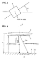
- the beam spot array is turned by turning the diffractive optical element 4 by the turning unit 5 about the optical axis of the element 4 in a plane orthogonal to across the optical axis so that the direction of the beam spot array is in agreement with that of the processing point array of the workpiece 7.
- the diffractive optical element 4 is set at an angle ⁇ by turning it about the optical axis
- the beam spot array is also turned by an angle ⁇ .
- the interval of the beam spot array is caused to be in agreement with that of the processing point array by adjusting the distance from the diffractive optical element 4 to the surface 7A of a workpiece 7 (or surface to be welded), using the moving unit 6.
- the focused beam spot formed by the first positive order diffracted beam is positioned as shown by an arrow B in FIG. 5.
- the direction and the interval of the array of the focused beam spots formed by the plurality of laser beams split by the diffractive optical element 4 are in agreement with those of the processing point array formed by the plurality of processing points.
- the focused beam spot formed by the zero-order laser beam which has passed through the diffractive optical element 4, to be in agreement with one of the processing points and then to cause the direction and and the interval of the array of focused beam spots to be in agreement with the counterparts of the array of processing points from the view point of workability and accuracy in the processing executed thereafter.
- the relationship between the distance Z from the diffractive optical element 4 to the surface 7A of the workpiece 7 to be processed and the spacing ⁇ between the zero-order beam spot and the first positive order beam spot will be explained with reference to FIG. 4.
- the relationship between the distance Z and the spacing ⁇ is given approximately by the following quation.
- ⁇ Z / Zmax ⁇ ⁇ max
- Zmax is a maximum value of the distance Z
- ⁇ max is a maximum value of the spacing ⁇ .
- the spacing ⁇ can be varied between 0 mm and 1.1 mm by changing the distance Z over the range of 0 to 90 mm.
- the distance Z may appropriately be varied in the range of 45 to 90 mm from a practical standpoint.
- solder means lead-free solder among others.
- the spacing ⁇ between the two focused beam spots can be varied from 0.55 to 1.1 mm. If the spacing ⁇ is adjustable in as wide a rangeas mentioned above, the laser processing apparatus can be effectively used for laser welding of parts onto a printed circuit board. If it is desirable to further widen the spacing ⁇ between the beam spots, the distance Zmax from the diffractive optical element 4 to the workpiece's surface 7A needs to be elongated. On the other hand, if the spacing ⁇ between the beam spots is desired to be narrowed, the distance Z should be decreased.
- the diffractive optical element 4 used in this embodiment is a one-dimensional relief grating that has a sawtooth-shaped cross section.
- the grating is formed on a fused silica substrate, which is sufficiently transparent at a wavelength chosen for use, by photolithography and dry etching.
- I 0 sin 2 ⁇ / 2 / ( ⁇ / 2 ⁇ ) 2
- I m sin 2 ⁇ 2 ⁇ ⁇ m - ⁇ / 2 / [ 2 ⁇ ⁇ m - ⁇ / 2 ⁇ ] 2
- I 0 and I m represent the zero-order beam intensity and the m-th order beam intensity respectively
- ⁇ shows the phase modulation depth of the grating
- ⁇ 2 ⁇ h(n - 1)/ ⁇ where n is the refractive index of a material and h is the depth of the grating.
- FIG. 2 shows the relationship between the diffraction order and the beam intensity of diffraction laser beams calculated using the equations (3-1) and (3-2).
- the zero-order beam and the first positive order beam have the same intensity of 0.405.
- a first negative order beam and a second positive order beam have the same intensity of 0.045
- a second negative order beam and a third positive order beam have the same intensity of 0.016.
- a laser utilization efficiency in solder welding is expected to be 81% that is sufficiently high from a practical standpoint.
- the intensities of the zero and first positive order beams used in solder welding are nine times or more higher than those of the other beams, there is no possibility that diffraction beams other than the zero and first positive order beams damage the surrownding areas around joint portions in consideration of a beam intensity necessary for solder welding.
- the intensity ratio between the two beams can be determined and varied from the design of the diffractive optical element, as needed.
- FIG. 6 is a view exemplifying a method of mounting a quartz oscillator 10 on a circuit board.
- the quartz oscillator 10 has two connection pins 11 and 12, and these connection pins 11 and 12 are inserted into terminals 21 and 22 on the board and connected thereto by solder welding.
- the terminals 21 and 22 used in the experiment has an interval of 0.80 mm, and the printed circuits 21A and 22A of the terminals are 0.30 mm wide.
- the laser beam intensity is adjusted appropriately to be so low as not to damage the board and the parts mounted thereon.
- any one of the terminals 21 and 22 is caused to be in agreement with the focused beam spot formed from the zero-order laser beam, which has passed through the diffractive optical element 4, making use of the optical axis positioning unit 8, and the like. Subsequently, the direction and the interval of the array of the focused beam spots formed from the split laser beams 2A are caused to be in agreement with those of the array of the terminals 21 and 22 using the above-described method.
- a solder is supplied to the connecting portions of the respective terminals 21 and 22 by a solder dispenser 9 set in the laser processing apparatus.
- the intensity of the two split laser beams 2A in which the position, the direction and the interval of the array of the focused beam spots formed thereby are caused to be in agreement with those of the array of the terminals 21 and 22 as described above, is raised by adjusting the output of the laser oscillator 1 up to a point that enables target processing to be executed.
- the split laser beams 2A are able to melt the solder.
- the connecting portions are simultaneously irradiated with the two split laser beams 2A whose intensity has been increased until the solder melts to thereby connect the connection pins 11 and 12 to the terminals 21 and 22 by welding.
- the quartz oscillator 10 is connected to the board.
- the solder since the solder is simultaneously heated at the two independent portions, the solder is melted and aggregated without problem.
- the solder welding portions are located close to each other as described above, if they are irradiated and heated with a single beam one by one, the solder at one portion under the laser irradiation heats up and tends to fuse with the solder at the other portion, meaning that the circuits may be short-circuited.
- This phenomenon may be also caused when the solders at the two welding portions are irradiated and heated alternately by scanning the beam because the scanning is executed at a limited speed. Such a problem can be also overcome by this embodiment.
- the directions and the intervals of the connection terminals of these parts may differ from each other. In this case, it is necessary to determine the position of the array of the focused beam spots to each of the positions where the quartz oscillators, the resistors, the capacitors, and the like are mounted. Further, when mounting parts, which are of the same type but have a different interval of pins, are jointed on the same board, the interval of the array of the focused beam spots must be adjusted by varying the distance between the diffractive optical element and the mounting board.
- FIG. 7 is a graph showing the relationship between the diffraction order and the beam intensity of split laser beams generated by another diffractive optical element 4A.
- the diffractive optical element 4A generates an array of seven laser beams, which are composed of from zero-th to sixth positive order having an equally spaced interval by splitting a single laser beam.
- the laser utilizing efficiency of the seven split laser beams is about 85% and the uniformity of the seven split beams is about 0.99, which exhibits sufficiently practical values.
- the diffractive optical element cannnot necessarily be realized in a saw-tooth shape and rather may be designed according to the necessary number of split of the laser beam and the distribution of intensity of the split laser beams. Accordingly, it is possible to use any one of positive or negative high order beams including a zero-order beam depending on the design of the diffractive optical element, and further it is also possible to more increase the laser utilization efficiency.
- FIG. 8 is a view exemplifying a case that a work is processed using the diffractive optical element 4A shown in the graph of FIG. 7.
- FIG. 8 shows an example that an IC 30 having connection pins 31 to 37 on one side are connected to a printed circuit board by laser soldering after inserting the pins 31 to 37 into the terminals 41 to 47 of the board corresponding thereto.
- reference numerals 41A to 47A denote printed circuits on the board that are connected to the respective terminals.
- the laser oscillator 1 emits a laser beam having low intensity so as not to damage the board and the parts mounted thereon.
- the array of the focused beam spots formed by the seven split laser beams 2A generated by the diffractive optical element 4A is caused to be in agreement with the array direction of the terminal 41 to 47 by turning the diffractive optical element 4A about its optical axis.
- the interval between the focused beam spots in the array is caused to be in agreement with the interval between the terminals 41 to 47 by moving the diffractive optical element 4A along an optical axis direction.
- the intensity of the seven split laser beams 2A in which the position, the direction and the interval of the array of the focused beam spots thereof are caused to be in agreement with those of the array of the terminals 41 to 47, is increased by adjusting the output of the laser oscillator 1, so that laser welding can be executed.
- the connecting portions are simultaneously irradiated with the seven split laser beams 2A whose intensity has been increased until the solder is melted to thereby connect the seven connection pins 31 to 37 on the one side of the IC 30 to the terminals 41 to 47 by welding.
- a pin array on the other side of the IC 30 is also connected to the board likewise. According to the above processing, the welding can be very effectively executed at the fourteen portions without thermally affecting the parts in the vicinity of the IC 30.
- a YAG laser (wavelength: 1.064 ⁇ m), a high-power semiconductor laser (wavelength: 0.808 ⁇ m, 0.940 ⁇ m) and the like can be used as a laser oscillator.
- various types of laser oscillators can be used according to demand for tose processes.
- the intensity of the split laser beams 2A is varied by changing the output of the laser oscillator 1.
- the intensity of the split laser beams 2A may be varied by fixing the output of the laser oscillator 1 and using other kinds of laser beam intensity changing means such as an attenuator and the like disposed outside the laser oscillator 1.
- the present invention can be also applied to processing using a two-dimensional array of split laser beams.
- the laser processing technology of the present invention easily realizes a good positional agreement between split beams and processing points, which is a serious issue in mass production, by considering a combination of the zero-order beam with higher order beams split by a diffractive optical element, and thus the present invention can be widely applied to the case that the direction of an array of processing points and the interval of the processing points are different in respective processing arrays.
- the solder welding of the mounting parts that are referred to in the above embodiment are only one example to which the present invention is applied, and the present invention can be also applied to various processing applications as well as the solder welding, such as, welding other than the solder welding, removing processing (drilling, groove cutting), property modification processing (alloying, polymerization, refraction factor modulation).
- the output and the irradiating time of laser may be appropriately determined according to a type of processing, when the processing points are simulatenously irradiatied with a plurality of split beams in which the positions, directions, and the interval of the array of focused beam spots are determined.
Landscapes
- Physics & Mathematics (AREA)
- Optics & Photonics (AREA)
- Engineering & Computer Science (AREA)
- Mechanical Engineering (AREA)
- Plasma & Fusion (AREA)
- Manufacturing & Machinery (AREA)
- Microelectronics & Electronic Packaging (AREA)
- Laser Beam Processing (AREA)
Applications Claiming Priority (3)
| Application Number | Priority Date | Filing Date | Title |
|---|---|---|---|
| JP2003025557 | 2003-02-03 | ||
| JP2003369929A JP3775410B2 (ja) | 2003-02-03 | 2003-10-30 | レーザー加工方法、レーザー溶接方法並びにレーザー加工装置 |
| EP04001892A EP1449610B1 (de) | 2003-02-03 | 2004-01-29 | Verfahren zur Laserbearbeitung und Vorrichtung zur Laserbearbeitung |
Related Parent Applications (1)
| Application Number | Title | Priority Date | Filing Date |
|---|---|---|---|
| EP04001892A Division EP1449610B1 (de) | 2003-02-03 | 2004-01-29 | Verfahren zur Laserbearbeitung und Vorrichtung zur Laserbearbeitung |
Publications (2)
| Publication Number | Publication Date |
|---|---|
| EP1803522A2 true EP1803522A2 (de) | 2007-07-04 |
| EP1803522A3 EP1803522A3 (de) | 2008-06-25 |
Family
ID=32737721
Family Applications (2)
| Application Number | Title | Priority Date | Filing Date |
|---|---|---|---|
| EP07006870A Withdrawn EP1803522A3 (de) | 2003-02-03 | 2004-01-29 | Laserverarbeitungsverfahren, Laserlötverfahren und Laserverarbeitungsvorrichtung |
| EP04001892A Expired - Lifetime EP1449610B1 (de) | 2003-02-03 | 2004-01-29 | Verfahren zur Laserbearbeitung und Vorrichtung zur Laserbearbeitung |
Family Applications After (1)
| Application Number | Title | Priority Date | Filing Date |
|---|---|---|---|
| EP04001892A Expired - Lifetime EP1449610B1 (de) | 2003-02-03 | 2004-01-29 | Verfahren zur Laserbearbeitung und Vorrichtung zur Laserbearbeitung |
Country Status (5)
| Country | Link |
|---|---|
| US (1) | US7009138B2 (de) |
| EP (2) | EP1803522A3 (de) |
| JP (1) | JP3775410B2 (de) |
| CN (1) | CN1314302C (de) |
| DE (1) | DE602004020817D1 (de) |
Cited By (1)
| Publication number | Priority date | Publication date | Assignee | Title |
|---|---|---|---|---|
| WO2012041711A1 (de) * | 2010-09-27 | 2012-04-05 | Jenoptik Optical Systems Gmbh | Anordnung und verfahren zur erzeugung eines lichtstrahles für die materialbearbeitung |
Families Citing this family (67)
| Publication number | Priority date | Publication date | Assignee | Title |
|---|---|---|---|---|
| JP3775410B2 (ja) * | 2003-02-03 | 2006-05-17 | セイコーエプソン株式会社 | レーザー加工方法、レーザー溶接方法並びにレーザー加工装置 |
| US7820936B2 (en) * | 2004-07-02 | 2010-10-26 | Boston Scientific Scimed, Inc. | Method and apparatus for controlling and adjusting the intensity profile of a laser beam employed in a laser welder for welding polymeric and metallic components |
| JP5420172B2 (ja) * | 2004-10-06 | 2014-02-19 | リモ パテントフェルヴァルトゥング ゲーエムベーハー ウント コー.カーゲー | レーザ装置 |
| KR20080017057A (ko) * | 2005-06-29 | 2008-02-25 | 코닌클리케 필립스 일렉트로닉스 엔.브이. | 레이저 용접 시스템과 방법 |
| US7626138B2 (en) * | 2005-09-08 | 2009-12-01 | Imra America, Inc. | Transparent material processing with an ultrashort pulse laser |
| DE102006038422A1 (de) * | 2006-08-17 | 2008-02-21 | Bayerische Motoren Werke Ag | Verfahren zum Verbinden mindestens zweier Werkstücke |
| JP2008221224A (ja) * | 2007-03-08 | 2008-09-25 | Nuclear Fuel Ind Ltd | レーザ溶接方法およびレーザ溶接装置 |
| CN101439431A (zh) * | 2007-11-21 | 2009-05-27 | 新科实业有限公司 | 多束激光接合机及接合方法 |
| FR2935621B1 (fr) * | 2008-09-05 | 2011-10-14 | John Sanjay Swamidas | Technique de brasage par laser holographie. |
| US8629843B2 (en) * | 2009-10-01 | 2014-01-14 | Blackberry Limited | Piezoelectric assembly |
| DE102010016628A1 (de) * | 2010-02-26 | 2011-09-29 | Reis Group Holding Gmbh & Co. Kg | Verfahren und Anordnung zum stoffschlüssigen Verbinden von Materialien |
| EP2478990B1 (de) | 2011-01-21 | 2019-04-17 | Leister Technologies AG | Verfahren zum Einstellen eines Laserlichtspots zur Laserbearbeitung von Werkstücken sowie Laseranordnung zur Durchführung des Verfahrens |
| US8951819B2 (en) * | 2011-07-11 | 2015-02-10 | Applied Materials, Inc. | Wafer dicing using hybrid split-beam laser scribing process with plasma etch |
| CN102500855B (zh) * | 2011-10-25 | 2014-06-25 | 深圳市联赢激光股份有限公司 | 一种用于半导体激光器的锡焊接方法 |
| WO2014079478A1 (en) | 2012-11-20 | 2014-05-30 | Light In Light Srl | High speed laser processing of transparent materials |
| EP2754524B1 (de) | 2013-01-15 | 2015-11-25 | Corning Laser Technologies GmbH | Verfahren und Vorrichtung zum laserbasierten Bearbeiten von flächigen Substraten, d.h. Wafer oder Glaselement, unter Verwendung einer Laserstrahlbrennlinie |
| EP2781296B1 (de) | 2013-03-21 | 2020-10-21 | Corning Laser Technologies GmbH | Vorrichtung und verfahren zum ausschneiden von konturen aus flächigen substraten mittels laser |
| KR20140118554A (ko) * | 2013-03-29 | 2014-10-08 | 삼성디스플레이 주식회사 | 광학계 및 기판 밀봉 방법 |
| US9701563B2 (en) | 2013-12-17 | 2017-07-11 | Corning Incorporated | Laser cut composite glass article and method of cutting |
| US11556039B2 (en) | 2013-12-17 | 2023-01-17 | Corning Incorporated | Electrochromic coated glass articles and methods for laser processing the same |
| US9850160B2 (en) | 2013-12-17 | 2017-12-26 | Corning Incorporated | Laser cutting of display glass compositions |
| US20150165560A1 (en) | 2013-12-17 | 2015-06-18 | Corning Incorporated | Laser processing of slots and holes |
| US10293436B2 (en) | 2013-12-17 | 2019-05-21 | Corning Incorporated | Method for rapid laser drilling of holes in glass and products made therefrom |
| US10442719B2 (en) | 2013-12-17 | 2019-10-15 | Corning Incorporated | Edge chamfering methods |
| US9815730B2 (en) | 2013-12-17 | 2017-11-14 | Corning Incorporated | Processing 3D shaped transparent brittle substrate |
| US9676167B2 (en) | 2013-12-17 | 2017-06-13 | Corning Incorporated | Laser processing of sapphire substrate and related applications |
| CN104923914B (zh) * | 2014-03-20 | 2017-08-22 | 大族激光科技产业集团股份有限公司 | 一种元器件引脚的焊接方法 |
| US10052719B2 (en) * | 2014-03-27 | 2018-08-21 | Primearth Ev Energy Co., Ltd. | Laser welding device, laser welding method, and battery casing |
| TWI730945B (zh) | 2014-07-08 | 2021-06-21 | 美商康寧公司 | 用於雷射處理材料的方法與設備 |
| EP3169479B1 (de) | 2014-07-14 | 2019-10-02 | Corning Incorporated | Verfahren und system zum stoppen von inzidenter rissausbreitung in einem transparenten material |
| WO2016010949A1 (en) | 2014-07-14 | 2016-01-21 | Corning Incorporated | Method and system for forming perforations |
| CN107073641B (zh) | 2014-07-14 | 2020-11-10 | 康宁股份有限公司 | 接口块;用于使用这种接口块切割在波长范围内透明的衬底的系统和方法 |
| KR20170028943A (ko) | 2014-07-14 | 2017-03-14 | 코닝 인코포레이티드 | 조정가능한 레이저 빔 촛점 라인을 사용하여 투명한 재료를 처리하는 방법 및 시스템 |
| US20170282295A1 (en) * | 2014-09-01 | 2017-10-05 | Toyota Motor Europe | Systems for and method of welding with a laser beam point linear profile obliquely oriented relative to the travel direction |
| JP6487184B2 (ja) * | 2014-11-10 | 2019-03-20 | 株式会社ディスコ | レーザー発振機構 |
| US10047001B2 (en) | 2014-12-04 | 2018-08-14 | Corning Incorporated | Glass cutting systems and methods using non-diffracting laser beams |
| CN107406293A (zh) | 2015-01-12 | 2017-11-28 | 康宁股份有限公司 | 使用多光子吸收方法来对经热回火的基板进行激光切割 |
| US11773004B2 (en) | 2015-03-24 | 2023-10-03 | Corning Incorporated | Laser cutting and processing of display glass compositions |
| KR20170131638A (ko) | 2015-03-27 | 2017-11-29 | 코닝 인코포레이티드 | 가스 투과성 유리창 및 이의 제작방법 |
| JP6510971B2 (ja) * | 2015-04-17 | 2019-05-08 | 日本特殊陶業株式会社 | 接合体の製造方法、及びスパークプラグの製造方法 |
| WO2017011296A1 (en) | 2015-07-10 | 2017-01-19 | Corning Incorporated | Methods of continuous fabrication of holes in flexible substrate sheets and products relating to the same |
| EP3184232B1 (de) * | 2015-12-23 | 2025-05-28 | Universität Stuttgart | Bohrvorrichtung, verfahren und verwendung |
| JP6938543B2 (ja) | 2016-05-06 | 2021-09-22 | コーニング インコーポレイテッド | 透明基板からの、輪郭設定された形状のレーザ切断及び取り外し |
| US10410883B2 (en) | 2016-06-01 | 2019-09-10 | Corning Incorporated | Articles and methods of forming vias in substrates |
| JP6808130B2 (ja) * | 2016-06-09 | 2021-01-06 | 福井県 | レーザ加工方法およびレーザ加工装置 |
| US10794679B2 (en) | 2016-06-29 | 2020-10-06 | Corning Incorporated | Method and system for measuring geometric parameters of through holes |
| CN109475976A (zh) * | 2016-07-14 | 2019-03-15 | 三菱电机株式会社 | 激光加工装置 |
| KR20190035805A (ko) | 2016-07-29 | 2019-04-03 | 코닝 인코포레이티드 | 레이저 처리를 위한 장치 및 방법 |
| KR102423775B1 (ko) | 2016-08-30 | 2022-07-22 | 코닝 인코포레이티드 | 투명 재료의 레이저 가공 |
| US10730783B2 (en) | 2016-09-30 | 2020-08-04 | Corning Incorporated | Apparatuses and methods for laser processing transparent workpieces using non-axisymmetric beam spots |
| KR102428350B1 (ko) | 2016-10-24 | 2022-08-02 | 코닝 인코포레이티드 | 시트형 유리 기판의 레이저 기반 기계 가공을 위한 기판 프로세싱 스테이션 |
| US10752534B2 (en) | 2016-11-01 | 2020-08-25 | Corning Incorporated | Apparatuses and methods for laser processing laminate workpiece stacks |
| JP2018092848A (ja) * | 2016-12-06 | 2018-06-14 | 日本特殊陶業株式会社 | スパークプラグの電極の製造方法、及び、スパークプラグの製造方法 |
| US10688599B2 (en) | 2017-02-09 | 2020-06-23 | Corning Incorporated | Apparatus and methods for laser processing transparent workpieces using phase shifted focal lines |
| US11078112B2 (en) | 2017-05-25 | 2021-08-03 | Corning Incorporated | Silica-containing substrates with vias having an axially variable sidewall taper and methods for forming the same |
| US10580725B2 (en) | 2017-05-25 | 2020-03-03 | Corning Incorporated | Articles having vias with geometry attributes and methods for fabricating the same |
| US10626040B2 (en) | 2017-06-15 | 2020-04-21 | Corning Incorporated | Articles capable of individual singulation |
| US12180108B2 (en) | 2017-12-19 | 2024-12-31 | Corning Incorporated | Methods for etching vias in glass-based articles employing positive charge organic molecules |
| US11554984B2 (en) | 2018-02-22 | 2023-01-17 | Corning Incorporated | Alkali-free borosilicate glasses with low post-HF etch roughness |
| TWI693119B (zh) * | 2019-03-06 | 2020-05-11 | 台灣愛司帝科技股份有限公司 | 應用於固接led的雷射加熱裝置 |
| CN112658423A (zh) * | 2019-10-15 | 2021-04-16 | 大族激光科技产业集团股份有限公司 | 一种多点同步锡焊方法和多点同步锡焊装置 |
| WO2021083487A1 (en) * | 2019-10-28 | 2021-05-06 | MAX-PLANCK-Gesellschaft zur Förderung der Wissenschaften e.V. | Laser system and method for driving a laser system |
| TWI754553B (zh) * | 2021-02-25 | 2022-02-01 | 東捷科技股份有限公司 | 焊接設備 |
| WO2022254807A1 (ja) * | 2021-06-02 | 2022-12-08 | ソニーグループ株式会社 | レーザーはんだ装置、制御装置及びレーザーはんだ付け方法 |
| WO2023281930A1 (ja) * | 2021-07-08 | 2023-01-12 | パナソニックIpマネジメント株式会社 | レーザ溶接装置、レーザ溶接方法及び回転電機の製造方法 |
| CN117500630A (zh) * | 2021-07-08 | 2024-02-02 | 松下知识产权经营株式会社 | 激光焊接装置、激光焊接方法以及旋转电机的制造方法 |
| CN113798705B (zh) * | 2021-09-07 | 2023-07-07 | 哈尔滨焊接研究院有限公司 | 一种大功率激光焊接特性高通量检测方法 |
Family Cites Families (12)
| Publication number | Priority date | Publication date | Assignee | Title |
|---|---|---|---|---|
| DE3831743A1 (de) * | 1988-09-17 | 1990-03-29 | Philips Patentverwaltung | Vorrichtung zur bearbeitung eines werkstueckes mit laserlicht und verwendung dieser vorrichtung |
| US6008914A (en) * | 1994-04-28 | 1999-12-28 | Mitsubishi Denki Kabushiki Kaisha | Laser transfer machining apparatus |
| JP2723798B2 (ja) * | 1994-04-28 | 1998-03-09 | 三菱電機株式会社 | レーザ転写加工装置 |
| JPH08279529A (ja) | 1995-04-05 | 1996-10-22 | Toshiba Corp | 電子部品実装装置及びはんだ付け方法 |
| JPH09199845A (ja) | 1996-01-19 | 1997-07-31 | Toshiba Corp | Yagレーザ加熱装置 |
| EP0838297A1 (de) * | 1996-08-20 | 1998-04-29 | MTA Automation AG | Lötkopf einer automatischen Lötanlage |
| JP2910720B2 (ja) | 1997-03-07 | 1999-06-23 | 日本電気株式会社 | はんだ付け方法 |
| JP4218209B2 (ja) * | 1999-03-05 | 2009-02-04 | 三菱電機株式会社 | レーザ加工装置 |
| JP2000280225A (ja) * | 1999-04-02 | 2000-10-10 | Murata Mfg Co Ltd | セラミックグリーンシートの加工方法及び加工装置 |
| IL133073A (en) * | 1999-11-22 | 2003-06-24 | Yaakov Amitai | Method and system for treating a target plane with a laser beam |
| JP3720681B2 (ja) * | 2000-06-26 | 2005-11-30 | 株式会社ファインディバイス | レーザー式はんだ付け方法及び装置 |
| JP3775410B2 (ja) * | 2003-02-03 | 2006-05-17 | セイコーエプソン株式会社 | レーザー加工方法、レーザー溶接方法並びにレーザー加工装置 |
-
2003
- 2003-10-30 JP JP2003369929A patent/JP3775410B2/ja not_active Expired - Fee Related
- 2003-12-30 CN CNB2003101243727A patent/CN1314302C/zh not_active Expired - Fee Related
-
2004
- 2004-01-29 DE DE602004020817T patent/DE602004020817D1/de not_active Expired - Lifetime
- 2004-01-29 EP EP07006870A patent/EP1803522A3/de not_active Withdrawn
- 2004-01-29 EP EP04001892A patent/EP1449610B1/de not_active Expired - Lifetime
- 2004-01-29 US US10/767,857 patent/US7009138B2/en not_active Expired - Lifetime
Cited By (1)
| Publication number | Priority date | Publication date | Assignee | Title |
|---|---|---|---|---|
| WO2012041711A1 (de) * | 2010-09-27 | 2012-04-05 | Jenoptik Optical Systems Gmbh | Anordnung und verfahren zur erzeugung eines lichtstrahles für die materialbearbeitung |
Also Published As
| Publication number | Publication date |
|---|---|
| CN1520249A (zh) | 2004-08-11 |
| JP3775410B2 (ja) | 2006-05-17 |
| EP1803522A3 (de) | 2008-06-25 |
| EP1449610A1 (de) | 2004-08-25 |
| DE602004020817D1 (de) | 2009-06-10 |
| US7009138B2 (en) | 2006-03-07 |
| US20050035102A1 (en) | 2005-02-17 |
| CN1314302C (zh) | 2007-05-02 |
| EP1449610B1 (de) | 2009-04-29 |
| JP2004255461A (ja) | 2004-09-16 |
Similar Documents
| Publication | Publication Date | Title |
|---|---|---|
| EP1449610B1 (de) | Verfahren zur Laserbearbeitung und Vorrichtung zur Laserbearbeitung | |
| US6639177B2 (en) | Method and system for processing one or more microstructures of a multi-material device | |
| JP2694026B2 (ja) | レーザ光加工装置 | |
| CA2000449C (en) | Diode laser soldering system | |
| TW202600274A (zh) | 雷射加工設備、其操作方法以及使用該雷射加工設備加工工件的方法 | |
| US20080047939A1 (en) | Process and apparatus for joining at least two elements | |
| JP2013132655A (ja) | レーザ半田付けシステム | |
| US10014657B2 (en) | Laser-machined optical components and related methods for pick and bond assembly | |
| KR20180104028A (ko) | 2차원의 신속한 온도 제어 환경에서 솔더 레지스트의 직접 노광을 위한 직접 노광 장치 | |
| JP2013103264A (ja) | レーザ半田付け装置及びその方法 | |
| KR20180060830A (ko) | 공간 광 변조기를 이용한 레이저 가공장치 | |
| JP4407202B2 (ja) | 加工装置及び加工方法とこれを用いた生産設備 | |
| CN113473718A (zh) | 一种电路板阻焊图案的制作方法 | |
| KR20230152776A (ko) | 레이저 가공 방법 및 레이저 가공 장치 | |
| CN101011779A (zh) | 激光加工方法、激光焊接方法及激光加工装置 | |
| JPS62263862A (ja) | レ−ザ加工装置 | |
| JPH04237589A (ja) | レーザ加工装置 | |
| KR20080019191A (ko) | 두 개 이상의 요소를 결합하기 위한 장치 및 방법 | |
| EP4718500A1 (de) | Verfahren und system zur manipulation von materialien und/oder komponenten unter verwendung eines gezielten lichtsystems | |
| JP7108345B2 (ja) | 電子装置の製造方法、マイクロニードルの製造方法及びマイクロニードル | |
| KR100826633B1 (ko) | 소자배열의 고속, 정밀한 마이크로머시닝을 위한 방법 및 시스템 | |
| JP2010052024A (ja) | 加工装置 | |
| JP2023173680A (ja) | ツインビーム半田付け装置 | |
| JPH0234272A (ja) | はんだ付け装置 | |
| JPH05329625A (ja) | 電子部品の光ビーム加工装置 |
Legal Events
| Date | Code | Title | Description |
|---|---|---|---|
| PUAI | Public reference made under article 153(3) epc to a published international application that has entered the european phase |
Free format text: ORIGINAL CODE: 0009012 |
|
| AC | Divisional application: reference to earlier application |
Ref document number: 1449610 Country of ref document: EP Kind code of ref document: P |
|
| AK | Designated contracting states |
Kind code of ref document: A2 Designated state(s): CH DE FR LI |
|
| PUAL | Search report despatched |
Free format text: ORIGINAL CODE: 0009013 |
|
| AK | Designated contracting states |
Kind code of ref document: A3 Designated state(s): CH DE FR LI |
|
| RIC1 | Information provided on ipc code assigned before grant |
Ipc: B23K 1/005 20060101AFI20070531BHEP Ipc: H05K 3/34 20060101ALI20080519BHEP Ipc: B23K 26/067 20060101ALI20080519BHEP |
|
| 17P | Request for examination filed |
Effective date: 20080709 |
|
| 17Q | First examination report despatched |
Effective date: 20080916 |
|
| AKX | Designation fees paid |
Designated state(s): CH DE FR LI |
|
| STAA | Information on the status of an ep patent application or granted ep patent |
Free format text: STATUS: THE APPLICATION IS DEEMED TO BE WITHDRAWN |
|
| 18D | Application deemed to be withdrawn |
Effective date: 20090127 |