EP1792346B1 - High-mobility bulk silicon pfet fabrication method - Google Patents
High-mobility bulk silicon pfet fabrication method Download PDFInfo
- Publication number
- EP1792346B1 EP1792346B1 EP05805693A EP05805693A EP1792346B1 EP 1792346 B1 EP1792346 B1 EP 1792346B1 EP 05805693 A EP05805693 A EP 05805693A EP 05805693 A EP05805693 A EP 05805693A EP 1792346 B1 EP1792346 B1 EP 1792346B1
- Authority
- EP
- European Patent Office
- Prior art keywords
- layer
- crystal silicon
- gate electrode
- region
- polysilicon
- Prior art date
- Legal status (The legal status is an assumption and is not a legal conclusion. Google has not performed a legal analysis and makes no representation as to the accuracy of the status listed.)
- Not-in-force
Links
- 238000004519 manufacturing process Methods 0.000 title claims abstract description 14
- 229910052710 silicon Inorganic materials 0.000 title claims description 28
- 239000010703 silicon Substances 0.000 title claims description 28
- XUIMIQQOPSSXEZ-UHFFFAOYSA-N Silicon Chemical compound [Si] XUIMIQQOPSSXEZ-UHFFFAOYSA-N 0.000 title claims description 25
- 238000000034 method Methods 0.000 title claims description 24
- 229910021421 monocrystalline silicon Inorganic materials 0.000 claims abstract description 78
- 239000000758 substrate Substances 0.000 claims abstract description 26
- 230000005669 field effect Effects 0.000 claims abstract description 8
- 229910021420 polycrystalline silicon Inorganic materials 0.000 claims description 41
- 229920005591 polysilicon Polymers 0.000 claims description 41
- 125000006850 spacer group Chemical group 0.000 claims description 38
- 239000013078 crystal Substances 0.000 claims description 15
- 230000001590 oxidative effect Effects 0.000 claims description 2
- VYPSYNLAJGMNEJ-UHFFFAOYSA-N Silicium dioxide Chemical compound O=[Si]=O VYPSYNLAJGMNEJ-UHFFFAOYSA-N 0.000 description 17
- 239000007943 implant Substances 0.000 description 16
- 238000005468 ion implantation Methods 0.000 description 16
- 239000002019 doping agent Substances 0.000 description 14
- 150000002500 ions Chemical class 0.000 description 10
- 238000001020 plasma etching Methods 0.000 description 9
- 229910052681 coesite Inorganic materials 0.000 description 8
- 229910052906 cristobalite Inorganic materials 0.000 description 8
- 239000000377 silicon dioxide Substances 0.000 description 8
- 229910052682 stishovite Inorganic materials 0.000 description 8
- 229910052905 tridymite Inorganic materials 0.000 description 8
- BLRPTPMANUNPDV-UHFFFAOYSA-N Silane Chemical compound [SiH4] BLRPTPMANUNPDV-UHFFFAOYSA-N 0.000 description 6
- 125000001475 halogen functional group Chemical group 0.000 description 6
- 238000004518 low pressure chemical vapour deposition Methods 0.000 description 6
- ZOXJGFHDIHLPTG-UHFFFAOYSA-N Boron Chemical compound [B] ZOXJGFHDIHLPTG-UHFFFAOYSA-N 0.000 description 5
- 229910003811 SiGeC Inorganic materials 0.000 description 5
- 229910000577 Silicon-germanium Inorganic materials 0.000 description 5
- 229910052785 arsenic Inorganic materials 0.000 description 5
- RQNWIZPPADIBDY-UHFFFAOYSA-N arsenic atom Chemical compound [As] RQNWIZPPADIBDY-UHFFFAOYSA-N 0.000 description 5
- 229910052796 boron Inorganic materials 0.000 description 5
- 229910052581 Si3N4 Inorganic materials 0.000 description 4
- 230000015572 biosynthetic process Effects 0.000 description 4
- 230000003647 oxidation Effects 0.000 description 4
- 238000007254 oxidation reaction Methods 0.000 description 4
- BOTDANWDWHJENH-UHFFFAOYSA-N Tetraethyl orthosilicate Chemical compound CCO[Si](OCC)(OCC)OCC BOTDANWDWHJENH-UHFFFAOYSA-N 0.000 description 3
- 238000009413 insulation Methods 0.000 description 3
- 239000012212 insulator Substances 0.000 description 3
- 238000002955 isolation Methods 0.000 description 3
- 239000000463 material Substances 0.000 description 3
- 230000003247 decreasing effect Effects 0.000 description 2
- 238000000151 deposition Methods 0.000 description 2
- QUZPNFFHZPRKJD-UHFFFAOYSA-N germane Chemical compound [GeH4] QUZPNFFHZPRKJD-UHFFFAOYSA-N 0.000 description 2
- 229910052986 germanium hydride Inorganic materials 0.000 description 2
- -1 halo ion Chemical class 0.000 description 2
- 239000000203 mixture Substances 0.000 description 2
- 229910052814 silicon oxide Inorganic materials 0.000 description 2
- OTMSDBZUPAUEDD-UHFFFAOYSA-N Ethane Chemical compound CC OTMSDBZUPAUEDD-UHFFFAOYSA-N 0.000 description 1
- 101001121408 Homo sapiens L-amino-acid oxidase Proteins 0.000 description 1
- 102100026388 L-amino-acid oxidase Human genes 0.000 description 1
- OAICVXFJPJFONN-UHFFFAOYSA-N Phosphorus Chemical compound [P] OAICVXFJPJFONN-UHFFFAOYSA-N 0.000 description 1
- 230000004888 barrier function Effects 0.000 description 1
- 230000000694 effects Effects 0.000 description 1
- 238000005530 etching Methods 0.000 description 1
- 125000001319 lambda(5)-arsanyl group Chemical group [H][As]([H])([H])([H])[*] 0.000 description 1
- UIUXUFNYAYAMOE-UHFFFAOYSA-N methylsilane Chemical compound [SiH3]C UIUXUFNYAYAMOE-UHFFFAOYSA-N 0.000 description 1
- 229910052698 phosphorus Inorganic materials 0.000 description 1
- 239000011574 phosphorus Substances 0.000 description 1
- 238000000206 photolithography Methods 0.000 description 1
- 229920002120 photoresistant polymer Polymers 0.000 description 1
- 238000005498 polishing Methods 0.000 description 1
Images


Classifications
-
- H—ELECTRICITY
- H10—SEMICONDUCTOR DEVICES; ELECTRIC SOLID-STATE DEVICES NOT OTHERWISE PROVIDED FOR
- H10D—INORGANIC ELECTRIC SEMICONDUCTOR DEVICES
- H10D62/00—Semiconductor bodies, or regions thereof, of devices having potential barriers
- H10D62/10—Shapes, relative sizes or dispositions of the regions of the semiconductor bodies; Shapes of the semiconductor bodies
- H10D62/13—Semiconductor regions connected to electrodes carrying current to be rectified, amplified or switched, e.g. source or drain regions
- H10D62/149—Source or drain regions of field-effect devices
- H10D62/151—Source or drain regions of field-effect devices of IGFETs
-
- H—ELECTRICITY
- H10—SEMICONDUCTOR DEVICES; ELECTRIC SOLID-STATE DEVICES NOT OTHERWISE PROVIDED FOR
- H10D—INORGANIC ELECTRIC SEMICONDUCTOR DEVICES
- H10D44/00—Charge transfer devices
- H10D44/40—Charge-coupled devices [CCD]
- H10D44/45—Charge-coupled devices [CCD] having field effect produced by insulated gate electrodes
-
- H—ELECTRICITY
- H10—SEMICONDUCTOR DEVICES; ELECTRIC SOLID-STATE DEVICES NOT OTHERWISE PROVIDED FOR
- H10D—INORGANIC ELECTRIC SEMICONDUCTOR DEVICES
- H10D30/00—Field-effect transistors [FET]
-
- H—ELECTRICITY
- H10—SEMICONDUCTOR DEVICES; ELECTRIC SOLID-STATE DEVICES NOT OTHERWISE PROVIDED FOR
- H10D—INORGANIC ELECTRIC SEMICONDUCTOR DEVICES
- H10D30/00—Field-effect transistors [FET]
- H10D30/40—FETs having zero-dimensional [0D], one-dimensional [1D] or two-dimensional [2D] charge carrier gas channels
- H10D30/47—FETs having zero-dimensional [0D], one-dimensional [1D] or two-dimensional [2D] charge carrier gas channels having 2D charge carrier gas channels, e.g. nanoribbon FETs or high electron mobility transistors [HEMT]
-
- H—ELECTRICITY
- H10—SEMICONDUCTOR DEVICES; ELECTRIC SOLID-STATE DEVICES NOT OTHERWISE PROVIDED FOR
- H10D—INORGANIC ELECTRIC SEMICONDUCTOR DEVICES
- H10D30/00—Field-effect transistors [FET]
- H10D30/60—Insulated-gate field-effect transistors [IGFET]
- H10D30/601—Insulated-gate field-effect transistors [IGFET] having lightly-doped drain or source extensions, e.g. LDD IGFETs or DDD IGFETs
-
- H—ELECTRICITY
- H10—SEMICONDUCTOR DEVICES; ELECTRIC SOLID-STATE DEVICES NOT OTHERWISE PROVIDED FOR
- H10D—INORGANIC ELECTRIC SEMICONDUCTOR DEVICES
- H10D30/00—Field-effect transistors [FET]
- H10D30/60—Insulated-gate field-effect transistors [IGFET]
- H10D30/751—Insulated-gate field-effect transistors [IGFET] having composition variations in the channel regions
-
- H—ELECTRICITY
- H10—SEMICONDUCTOR DEVICES; ELECTRIC SOLID-STATE DEVICES NOT OTHERWISE PROVIDED FOR
- H10D—INORGANIC ELECTRIC SEMICONDUCTOR DEVICES
- H10D30/00—Field-effect transistors [FET]
- H10D30/60—Insulated-gate field-effect transistors [IGFET]
- H10D30/791—Arrangements for exerting mechanical stress on the crystal lattice of the channel regions
- H10D30/797—Arrangements for exerting mechanical stress on the crystal lattice of the channel regions being in source or drain regions, e.g. SiGe source or drain
-
- H—ELECTRICITY
- H10—SEMICONDUCTOR DEVICES; ELECTRIC SOLID-STATE DEVICES NOT OTHERWISE PROVIDED FOR
- H10D—INORGANIC ELECTRIC SEMICONDUCTOR DEVICES
- H10D62/00—Semiconductor bodies, or regions thereof, of devices having potential barriers
- H10D62/01—Manufacture or treatment
- H10D62/021—Forming source or drain recesses by etching e.g. recessing by etching and then refilling
-
- H—ELECTRICITY
- H10—SEMICONDUCTOR DEVICES; ELECTRIC SOLID-STATE DEVICES NOT OTHERWISE PROVIDED FOR
- H10D—INORGANIC ELECTRIC SEMICONDUCTOR DEVICES
- H10D62/00—Semiconductor bodies, or regions thereof, of devices having potential barriers
- H10D62/10—Shapes, relative sizes or dispositions of the regions of the semiconductor bodies; Shapes of the semiconductor bodies
- H10D62/113—Isolations within a component, i.e. internal isolations
- H10D62/115—Dielectric isolations, e.g. air gaps
- H10D62/116—Dielectric isolations, e.g. air gaps adjoining the input or output regions of field-effect devices, e.g. adjoining source or drain regions
-
- H—ELECTRICITY
- H10—SEMICONDUCTOR DEVICES; ELECTRIC SOLID-STATE DEVICES NOT OTHERWISE PROVIDED FOR
- H10D—INORGANIC ELECTRIC SEMICONDUCTOR DEVICES
- H10D62/00—Semiconductor bodies, or regions thereof, of devices having potential barriers
- H10D62/10—Shapes, relative sizes or dispositions of the regions of the semiconductor bodies; Shapes of the semiconductor bodies
- H10D62/17—Semiconductor regions connected to electrodes not carrying current to be rectified, amplified or switched, e.g. channel regions
- H10D62/351—Substrate regions of field-effect devices
- H10D62/357—Substrate regions of field-effect devices of FETs
- H10D62/364—Substrate regions of field-effect devices of FETs of IGFETs
- H10D62/371—Inactive supplementary semiconductor regions, e.g. for preventing punch-through, improving capacity effect or leakage current
-
- H—ELECTRICITY
- H10—SEMICONDUCTOR DEVICES; ELECTRIC SOLID-STATE DEVICES NOT OTHERWISE PROVIDED FOR
- H10D—INORGANIC ELECTRIC SEMICONDUCTOR DEVICES
- H10D64/00—Electrodes of devices having potential barriers
- H10D64/20—Electrodes characterised by their shapes, relative sizes or dispositions
- H10D64/23—Electrodes carrying the current to be rectified, amplified, oscillated or switched, e.g. sources, drains, anodes or cathodes
- H10D64/251—Source or drain electrodes for field-effect devices
- H10D64/258—Source or drain electrodes for field-effect devices characterised by the relative positions of the source or drain electrodes with respect to the gate electrode
- H10D64/259—Source or drain electrodes being self-aligned with the gate electrode and having bottom surfaces higher than the interface between the channel and the gate dielectric
-
- H—ELECTRICITY
- H10—SEMICONDUCTOR DEVICES; ELECTRIC SOLID-STATE DEVICES NOT OTHERWISE PROVIDED FOR
- H10D—INORGANIC ELECTRIC SEMICONDUCTOR DEVICES
- H10D84/00—Integrated devices formed in or on semiconductor substrates that comprise only semiconducting layers, e.g. on Si wafers or on GaAs-on-Si wafers
- H10D84/01—Manufacture or treatment
- H10D84/0123—Integrating together multiple components covered by H10D12/00 or H10D30/00, e.g. integrating multiple IGBTs
- H10D84/0126—Integrating together multiple components covered by H10D12/00 or H10D30/00, e.g. integrating multiple IGBTs the components including insulated gates, e.g. IGFETs
- H10D84/0165—Integrating together multiple components covered by H10D12/00 or H10D30/00, e.g. integrating multiple IGBTs the components including insulated gates, e.g. IGFETs the components including complementary IGFETs, e.g. CMOS devices
- H10D84/0167—Manufacturing their channels
-
- H—ELECTRICITY
- H10—SEMICONDUCTOR DEVICES; ELECTRIC SOLID-STATE DEVICES NOT OTHERWISE PROVIDED FOR
- H10D—INORGANIC ELECTRIC SEMICONDUCTOR DEVICES
- H10D84/00—Integrated devices formed in or on semiconductor substrates that comprise only semiconducting layers, e.g. on Si wafers or on GaAs-on-Si wafers
- H10D84/01—Manufacture or treatment
- H10D84/0123—Integrating together multiple components covered by H10D12/00 or H10D30/00, e.g. integrating multiple IGBTs
- H10D84/0126—Integrating together multiple components covered by H10D12/00 or H10D30/00, e.g. integrating multiple IGBTs the components including insulated gates, e.g. IGFETs
- H10D84/0165—Integrating together multiple components covered by H10D12/00 or H10D30/00, e.g. integrating multiple IGBTs the components including insulated gates, e.g. IGFETs the components including complementary IGFETs, e.g. CMOS devices
- H10D84/017—Manufacturing their source or drain regions, e.g. silicided source or drain regions
-
- H—ELECTRICITY
- H10—SEMICONDUCTOR DEVICES; ELECTRIC SOLID-STATE DEVICES NOT OTHERWISE PROVIDED FOR
- H10D—INORGANIC ELECTRIC SEMICONDUCTOR DEVICES
- H10D84/00—Integrated devices formed in or on semiconductor substrates that comprise only semiconducting layers, e.g. on Si wafers or on GaAs-on-Si wafers
- H10D84/01—Manufacture or treatment
- H10D84/0123—Integrating together multiple components covered by H10D12/00 or H10D30/00, e.g. integrating multiple IGBTs
- H10D84/0126—Integrating together multiple components covered by H10D12/00 or H10D30/00, e.g. integrating multiple IGBTs the components including insulated gates, e.g. IGFETs
- H10D84/0165—Integrating together multiple components covered by H10D12/00 or H10D30/00, e.g. integrating multiple IGBTs the components including insulated gates, e.g. IGFETs the components including complementary IGFETs, e.g. CMOS devices
- H10D84/0188—Manufacturing their isolation regions
-
- H—ELECTRICITY
- H10—SEMICONDUCTOR DEVICES; ELECTRIC SOLID-STATE DEVICES NOT OTHERWISE PROVIDED FOR
- H10D—INORGANIC ELECTRIC SEMICONDUCTOR DEVICES
- H10D84/00—Integrated devices formed in or on semiconductor substrates that comprise only semiconducting layers, e.g. on Si wafers or on GaAs-on-Si wafers
- H10D84/01—Manufacture or treatment
- H10D84/02—Manufacture or treatment characterised by using material-based technologies
- H10D84/03—Manufacture or treatment characterised by using material-based technologies using Group IV technology, e.g. silicon technology or silicon-carbide [SiC] technology
- H10D84/038—Manufacture or treatment characterised by using material-based technologies using Group IV technology, e.g. silicon technology or silicon-carbide [SiC] technology using silicon technology, e.g. SiGe
-
- H—ELECTRICITY
- H10—SEMICONDUCTOR DEVICES; ELECTRIC SOLID-STATE DEVICES NOT OTHERWISE PROVIDED FOR
- H10D—INORGANIC ELECTRIC SEMICONDUCTOR DEVICES
- H10D62/00—Semiconductor bodies, or regions thereof, of devices having potential barriers
- H10D62/80—Semiconductor bodies, or regions thereof, of devices having potential barriers characterised by the materials
- H10D62/82—Heterojunctions
- H10D62/822—Heterojunctions comprising only Group IV materials heterojunctions, e.g. Si/Ge heterojunctions
-
- H—ELECTRICITY
- H10—SEMICONDUCTOR DEVICES; ELECTRIC SOLID-STATE DEVICES NOT OTHERWISE PROVIDED FOR
- H10D—INORGANIC ELECTRIC SEMICONDUCTOR DEVICES
- H10D64/00—Electrodes of devices having potential barriers
- H10D64/01—Manufacture or treatment
- H10D64/021—Manufacture or treatment using multiple gate spacer layers, e.g. bilayered sidewall spacers
-
- H—ELECTRICITY
- H10—SEMICONDUCTOR DEVICES; ELECTRIC SOLID-STATE DEVICES NOT OTHERWISE PROVIDED FOR
- H10D—INORGANIC ELECTRIC SEMICONDUCTOR DEVICES
- H10D84/00—Integrated devices formed in or on semiconductor substrates that comprise only semiconducting layers, e.g. on Si wafers or on GaAs-on-Si wafers
- H10D84/01—Manufacture or treatment
- H10D84/02—Manufacture or treatment characterised by using material-based technologies
- H10D84/03—Manufacture or treatment characterised by using material-based technologies using Group IV technology, e.g. silicon technology or silicon-carbide [SiC] technology
- H10D84/035—Manufacture or treatment characterised by using material-based technologies using Group IV technology, e.g. silicon technology or silicon-carbide [SiC] technology using silicon carbide [SiC] technology
Definitions
- the present invention relates to the field of field effect transistors (FETs); more specifically, it relates to methods of fabricating high-mobility PFETs.
- CMOS Complimentary metal-oxide-silicon
- CMOS technology utilizes n-channel metal-oxide-silicon field effect transistors (n-MOSFETs) often shortened to NFETs and p-channel metal-oxide-silicon field effect transistors (p-MOSFETs) often shortened to PFETs.
- NFETs and PFETs are well known in the art and comprise a source region and a drain region on opposite sides of a channel region formed in single-crystal silicon with a gate electrode formed on top of a gate dielectric layer which is itself formed on top of the channel region.
- the PFETs need to be larger than the NFETs to overcome the difference in carrier mobility between NFETs and PFETs so as not to let the PFETs limit overall circuit switching speed.
- the hole mobility in PFETs is about 25% that of the electron mobility of NFETs. Larger PFETs require more silicon area and more power in a time when modem integrated circuits need to be smaller and consume less power in very many applications.
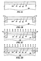
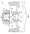
- FIG. 1 is a cross-sectional view of a PFET 100 fabricated according to a method of the present invention.
- FIG. 1 is a cross-section along the channel length direction of PFET 100.
- PFET 100 includes a gate 105; an N-doped single-crystal silicon region 110 under gate 105, a P-doped polysilicon source region 120A abutting shallow trench isolation (STI) 115 (that bounds PFET 100 but is technically not part of PFET 100); a single-crystal silicon source region 125A extending into single-crystal silicon region 110 (bounded by the dashed lines) and extending under gate 105; a P-doped polysilicon drain region 120B abutting STI 115; and a P-doped single-crystal silicon drain region 125B abutting polysilicon drain region 120B and extending into single-crystal silicon region 110 (bounded by the dashed lines) and extending under gate 105
- PFET 100 further includes a buried dielectric layer 130A under polysilicon source region 120A and single-crystal silicon source region 125A and extending from STI 115 to under gate 105; and a buried dielectric layer 130B under drain region 120B and single-crystal silicon drain region 125B and extending from STI 115 to under gate 105.
- PFET 100 still further includes a single-crystal Ge comprising layer 135 under single-crystal silicon region 110 and extending between buried dielectric layers 130A and 130B; an N-well 145 under buried dielectric layers 130A and 130B and Ge comprising layer 135; and a retrograde N-type ion-implant peak 140 in a single-crystal silicon N-well 145 (in a silicon substrate 150) under buried dielectric layers 130A and 130B and Ge comprising layer 135 and bounded by STI 115.
- polysilicon source region 120A and single-crystal silicon source region 125A are physically and electrically in contact and structurally and electrically comprise the source of PFET 100.
- polysilicon drain region 120B and single-crystal silicon drain region 125B are physically and electrically in contact and structurally and electrically comprise the drain of PFET 100.
- Gate 105 includes a gate dielectric layer 155 on a top surface 160 of single-crystal silicon region 110 and a P-doped or undoped polysilicon gate electrode 165 on a top surface 170 of gate dielectric layer 155 and a capping layer 175 on a top surface 180 of gate electrode 165.
- Optional sidewall insulation layers 185A and 185B are formed on opposing sidewalls 190A and 190B respectively of gate electrode 165 and dielectric spacers 195A and 195B are formed on outer surfaces 200A and 200B respectively of corresponding sidewall insulation layers 185A and 185B.
- Gate dielectric layer 155 is illustrated in FIG. 1 extending under spacers 195A and 195B. Alternatively, gate dielectric layer may extend partially or not at all under spacers 195A and 195B.
- a channel region 205 is defined in single-crystal silicon region 110.
- Channel region 205 may include a portion of adjacent to top surface 160 of substrate 150 between single-crystal silicon source region 125A and single-crystal silicon drain region 125B or channel region 205 may include all of single-crystal silicon region 110 between single-crystal silicon source region 125A and single-crystal silicon drain region 125B.
- Single-crystal silicon region 110 extends under spacers 195A and 195B as illustrated in FIG. 1 or may extend under and past spacers 195A and 195B toward STI 115.
- Buried dielectric layer 130A includes a first region 210A and a second region 215A.
- Second region 215A is thicker than first region 210A.
- First region 210A extends under polysilicon source region 120A from STI 115 to meet second region 215A under spacer 195A.
- Second region 215A extends from first region 210A from under spacer 195A to Ge comprising layer 135 under gate 105.
- Buried dielectric layer 130B includes a first region 210B and a second region 215B.
- Second region 215B is thicker than first region 210B.
- First region 210B extends under polysilicon drain region 120B from STI 115 to meet second region 215A under spacer 195B.
- Second region 215B extends from first region 210B from under spacer 195A to Ge comprising layer 135 under gate 105.
- a top surface 220A of second region 215A slopes upward (toward surface 160 of substrate 150) from Ge comprising layer 135 to meet polysilicon source region 120A under spacer 195A.
- a bottom surface 225A of second region 215A slopes downward (away from surface 160 of substrate 150) from Ge comprising layer 135 to meet first region 210A under spacer 195A.
- a top surface 220B of second region 215B slopes upward from Ge comprising layer 135 to meet polysilicon drain region 120B under spacer 195B.
- a bottom surface 225B of second region 215B slopes downward from Ge comprising layer 135 to meet first region 210B under spacer 195B.
- top surface 220A of second region 215A of buried dielectric layer 130A and of top surface 220B of second region 215B of buried dielectric layer 130B which is in the order of 50% percent from flat (relative to top surface 160 of substrate 150) imparts a stress of about 50 mega-pascals to about 1000 mega-pascals to the crystal lattice of single-crystal silicon region 110 and channel region 205.
- Stress on silicon the silicon lattice of PFETs has been shown to increase the hole mobility and thus the drain current of the PFET which can be advantageously used to reduce the silicon area of a PFET required for a given PFET drain current rating.
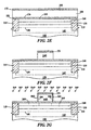
- FIGs. 2A through 2P are cross-sectional views illustrating fabrication of PFET 100 of FIG. 1 .
- single-crystal silicon substrate 150 has a Ge comprising layer 135 formed on a top surface 230 of a single-crystal silicon substrate 150 and a single-crystal silicon layer 240 formed on a top surface 235 of Ge comprising layer 135.
- Single-crystal silicon substrates are also called mono-crystalline silicon substrates or bulk silicon substrates.
- Ge comprising layer 135 comprises Si (1-X) Ge X where X equals about 0.15 to about 0.5.
- Ge comprising layer 135 comprises Si (1-X-Y )Ge X C Y where X equals about 0.15 to about 0.5 and Y equals about 0 to about 0.1.
- a single-crystal SiGe layer may be epitaxially formed by low pressure chemical vapor deposition (LPCVD) using SiH 4 and GeH 4 .
- a single-crystal SiGeC layer may be epitaxially formed by LPCVD using a combination of SiH 4 , GeH 4 and CH 3 SiH 3 or C 2 H 6 .
- Ge comprising layer 135 is about 10 nm to about 100 nm thick.
- a single-crystal silicon layer may be epitaxially formed by LPCVD using SiH 4 and/or H 2 .
- single-crystal silicon layer 240 is about 5 nm to about 50 nm thick.
- STI 115 is formed.
- STI 115 extends from a top surface 245 of single-crystal silicon layer 240 through single-crystal silicon layer 240, through single-crystal Ge comprising layer 135 into substrate 150.
- STI 115 may be formed by reactive ion etching (RIE) trenches through single-crystal Ge comprising layer 135 into substrate 150, depositing an insulator such as SiO 2 or tetraethoxysilane (TEOS) oxide to fill the resultant trench and chemical-mechanical polishing (CMP) down to top surface 245 of single-crystal silicon layer 240 to remove excess insulator.
- RIE reactive ion etching
- N-well 145 is formed in substrate 150 by ion implantation of an N-dopant such as arsenic or phosphorus. While N-well 145 is illustrated as extending below STI 145, N-well 145 may be about even with or shallower than the STI.
- a retrograde ion implantation is performed using an N-dopant such as arsenic.
- a retrograde ion implant is defined as an ion implant having a peak concentration below a surface of the material into which the ion implantation is performed. Peak 140 of the retrograde ion implant is located a distance D below top surface 235 of Ge comprising layer 240.
- gate dielectric layer 155 is formed on top surface 245 of single-crystal silicon layer 240.
- gate dielectric layer 155 comprises deposited or thermal SiO 2 , but may be any gate dielectric known in the art.
- An N-doped or undoped polysilicon layer 250 is formed on top surface 170 of gate dielectric layer 155.
- Polysilicon may be formed by CVD using SiH 4 (and optionally AsH 4 or PH 4 if the gate is to be doped at this point in the fabrication).
- Capping layer 175 is formed on a top surface 255 of polysilicon layer 250.
- capping layer 175 comprises a TEOS oxide layer over a thermal SiO 2 layer.
- capping layer 175 is patterned and used as a hard mask to etch away undesired portions of polysilicon layer 250 (see FIG. 2E ) to form gate electrode 165 under remaining capping layer 175.
- an optional sidewall isolation layer 185 is formed on sidewalls 190 of gate electrode 165.
- an optional P-dopant extension ion implant using, for example, boron and/or an optional N-dopant halo ion implant using, for example, arsenic is performed to form extension/halo regions 260 in single-crystal silicon layer 240.
- Extension and halo implants may be performed at an angle of other than 90° relative to top surface 245 of single-crystal silicon layer 240.
- the halo and extension implants are performed such that, while they extend under gate electrode 165, they will not extend as far as thick regions 215A and 215B of respective buried dielectric layers 130A and 130B extend under the gate electrode (see FIG. 1 ).
- the halo and extension implants are shallow implants and do not extend below Ge comprising layer 135.
- extension and/or halo ion implants may be performed after formation of gate electrode 165 but before formation of sidewall isolation layer 185.
- spacers 195 are formed on outer surfaces 200 of sidewall insulation layer 185.
- Spacers195 may comprise Si 3 N 4 , SiO 2 , or combinations thereof.
- spacers 195 may comprise a multiple overlaid spacers, each spacer formed from either SiO 2 and Si 3 N 4 .
- one or both of the halo and extension ion implants discussed supra, may be alternatively, performed after formation of spacers 195.
- Spacers are formed by depositing a conformal layer of material and then performing an RIE process. Gate dielectric layer 155, not protected by gate electrode 165 and spacers 195 may also be removed by the RIE process or another process.
- Ge comprising layer 135 is etched to recess the Ge comprising layer in regions where single-crystal silicon layer 240 were removed, so that Ge comprising layer 135 is thinner in these regions than under gate electrode 165 and spacers 195.
- Ge comprising layer 135 is thinned to half its original thickness where not protected by gate electrode 165 and spacers 195.
- Ge comprising layer 135 is thinned to between about 5 nm to about 50 nm where not protected by gate electrode 165 and spacers 195.
- the etching of single-crystal silicon layer 240 and Ge comprising layer 135 may be accomplished using an RIE process that selectively etches Si, SiGe and SiGeC relative to the material of capping layer 175, spacers 195, and STI 115.
- a suitable RIE process would utilize a mixture of CF 4 and O 2 .
- Ge comprising layer 135 is oxidized to form buried dielectric layer 130 which comprises oxides of Si and Ge.
- an oxidation at about 600°C or less using a mixture of H 2 O vapor and O 2 is performed.
- single-crystal SiGe and single-crystal SiGeC oxidize about 40 times faster than single-crystal silicon.
- the volume of the oxidized SiGe or SiGeC about doubles with about 40% of the volume being below the original surface and about 60% of the volume being above the original surface.
- Ge comprising layer 135 oxidizes horizontally under spacers 195 and gate electrode 165 a distance equal to the thickness of oxidized SiGe or SiGeC formed where Ge comprising layer 135 was not protected by gate electrode 165 and spacers 195. It should also be remembered that Ge comprising layer 135 was thicker under spacers 195 and gate electrode 165 than where the Ge comprising layer was exposed. Therefore, buried dielectric layer 130 includes a thick region 215 under spacers 195 and extending partially under gate electrode 165 and a thin region 210 where buried dielectric layer 130 is not under spacers 195 and gate electrode 165.
- thin region 210 of buried dielectric layer 130 is about 10 nm to about 100 nm thick
- thick region 215 of buried dielectric layer 130 is about 10 nm to about 200 nm thick and extends under spacers 195 about 10 nm to about 200 nm.
- the only remaining Ge comprising layer 135 is an island under gate electrode 165. Also a thin layer of SiO 2 265 is formed on exposed edges of single-crystal silicon layer 240.
- a effect of the oxidation process is that regions of single-crystal silicon layer 240 between thick region 215 of buried dielectric layer 130 and gate dielectric layer 155 under spacers 195 are strained, that is, the crystal lattice is distorted from normal.
- thin layer of SiO 2 265 (see FIG. 2J ) is removed to expose edges 270 of single-crystal silicon region 240.
- epitaxial silicon regions 275 are grown on edges 270 (see FIG. 2K ) of single-crystal silicon region 240.
- epitaxial Si may be grown by LPCVD using SiH 4 .
- a polysilicon layer 280 is formed of sufficient thickness to cover capping layer 175 and spacers 195. As described supra, polysilicon layer 280 may be doped P-type or undoped. Epitaxial regions 275 on single-crystal silicon layer 240 (see FIG. 2L ) may increase in size slightly and single-crystal silicon region 110 results (see also FIG. 1 ).
- a CMP process is performed so that a top surface 285 of polysilicon layer 280 is coplanar with a top surface 290 of capping layer 175.
- a RIE etch back process is performed, so that polysilicon layer 280 (see FIG. 2N ) is removed from spacers 195, exposed ends of gate dielectric layer 155 and a top surface 295 of STI 115. Polysilicon layer 280 remains in the space defined by single-crystal silicon region 110, buried dielectric layer 130 and STI 115.
- an optional P-type (for example boron) ion implantation is performed to form P-doped polysilicon source/drains 120 in remaining polysilicon layer 280 (see FIG 280).
- the P-type ion implant may also be used to dope gate electrode 165. If polysilicon layer 280 was P-doped as deposited, this P-type ion implantation may be eliminated or not depending upon whether it is desired to P-type ion implant gate electrode 165.
- the structure of PFET 100 improves several operational parameters of the PFET.
- the relatively shallow single-crystal silicon region 110 under gate electrode 165, particularly near sidewalls 190A and 190B of the gate electrode result in improved short channel characteristics such as decreased sub-threshold voltage swing (S SWING ), decreased drain induced barrier loading, and more precise threshold voltage (V T ) control.
- the relatively deep polysilicon source and drain regions 120A and 120B result in lower source/drain resistance.
- buried dielectric layers 130A and 130B lower source/drain capacitance (compared to a conventional bulk silicon PFET).
- Ge comprising layer 135 between second region 215A of buried dielectric layer 130A and second region 215B of buried dielectric layer 130B (because of the high Ge doping levels) allows control of V T by voltage biasing N-well 145.
- These improved operating parameters have been experimentally shown to result in a significantly faster PFET (when compared to a conventional bulk silicon PFET of about the same channel width and channel length as a PFET fabricated according to the method of the present invention) and results in up to about a 42% increase in drain region current at saturation (I DSAT ) on short channel length devices. Fabrication of a PFET according to the present invention is essentially complete.
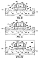
- FIGs. 3A through 3D are cross-sectional views illustrating fabrication of an NFET 300 (see FIG. 4 ) that may be fabricated alone or simultaneously with PFET 100 (see FIG 1 ). by several changes to the PFET process described supra . Before describing these changes, it should be understood, that it is well known in the art, that when both PFETs and NFETs are being fabricated on the same substrate, that the PFETs are protected from ion implantation during ion implants required only for the NFETs and that NFETs are protected from ion implantation during ion implants required only for the PFETs. Often this protection is provided by a photo resist layer.
- NFET 300 Fabrication of NFET 300 (see FIG. 4 ) alone or simultaneously with PFET 100 (see FIG. 1 ) is similar to the fabrication of PFET 100 (see FIG. 1 ) illustrated in FIGs. 2A through 2M and described supra, with the differences described immediately infra
- N-well 145 is replaced by a P-Well formed by ion implantation of a P-dopant such as boron.
- the N-doped retrograde ion implantation is replaced with a P-dopant retrograde ion implantation using a P-dopant species such as boron.
- FIG. 2C N-well 145 is replaced by a P-Well formed by ion implantation of a P-dopant such as boron.
- the N-doped retrograde ion implantation is replaced with a P-dopant retrograde ion implantation using a P-dopant species such as boron.
- the P-dopant extension ion implantation is replaced with an N-dopant extension ion implantation using an N-dopant species such as arsenic and the optional N-dopant halo ion implantation is replaced with a P-dopant ion extension ion implantation using a P-dopant species such as boron.
- FIGs. 3A and 3B are performed.
- a directional RIE is performed to remove thin region 210 of buried dielectric layer 130 not protected by spacer 195, capping layer 175 and gate electrode 165.
- capping layer 175 may be alternatively formed from Si 3 N 4 or layers of Si 3 N 4 and SiO 2 .
- FIG. 3B a isotropic silicon etch is performed to remove exposed portions of silicon substrate and undercut thick regions 215 of dielectric layer 130.
- STI 115 is not undercut. Removing silicon from under undercut thick regions 215 of dielectric layer 130 removes most or all of the stress previously induced into single-crystal silicon region 110 and channel region 205 (see FIG. 4 ).
- FIG. 2L is replaced with FIG. 3C and FIG. 2O is replaced with FIG. 3D .
- FIG. 3C epitaxial silicon regions 275 are grown on edges 270 (see FIG. 2K ) of single-crystal silicon region 240 and an epitaxial layer 285 is grown on exposed surface of silicon substrate 215.
- epitaxial Si may be grown by LPCVD using SiH 4 .
- a RIE etch back process is performed, so that polysilicon layer 280 (see FIG. 2N ) is removed from spacers 195, exposed ends of gate dielectric layer 155 and a top surface 295 of STI 115.
- a polysilicon layer 290 remains in the space defined by single-crystal silicon region 110, thick region 215 of buried dielectric layer 130, epitaxial layer 285 and STI 115.
- the optional P-type ion implantation is replaced with an optional N-type ion implantation (for example using arsenic) to form N-doped source/drains 120.
- Fabrication of an NFET according to the present invention is essentially complete.
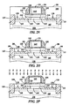
- FIG. 4 is a cross-sectional view of NFET 300 that may be fabricated alone or simultaneously with PFET 300 of FIG 1 , according to the present invention.
- FIG. 4 is similar to FIG 1 , except for several differences.
- single crystal region 110 is P-doped, instead of N-doped, source and drain regions 120A and 120B are N-doped instead of P-doped, single crystal regions 125A and B are N-doped instead of P-doped, N-well 145 is replaced with a P-well 145.
- epitaxial layers 285A and 285B intervene between respective polysilicon source/drain regions 120A and 120B and silicon substrate 150 rather than respective thin regions 210A and 210B (see FIG. 1 ) of dielectric layers 130A and 130B, and epitaxial layers 285A and 285B extend under respective thick regions 215A and 215B of dielectric layers 130A and 130B.
- Source/drain dopant species from source 120A and drain 120B may or may not extend into respective epitaxial layers 285A and 285B.
- the present invention provides a method of fabricating both an improved PFET with high switching speed at reduced silicon area and power consumption compared to conventional PFETs and an NFET that may be fabricated simultaneously with the improved PFET.
Landscapes
- Thin Film Transistor (AREA)
- Metal-Oxide And Bipolar Metal-Oxide Semiconductor Integrated Circuits (AREA)
- Insulated Gate Type Field-Effect Transistor (AREA)
Applications Claiming Priority (2)
| Application Number | Priority Date | Filing Date | Title |
|---|---|---|---|
| US10/711,453 US7078722B2 (en) | 2004-09-20 | 2004-09-20 | NFET and PFET devices and methods of fabricating same |
| PCT/US2005/033472 WO2006034189A2 (en) | 2004-09-20 | 2005-09-19 | High-mobility bulk silicon pfet |
Publications (3)
| Publication Number | Publication Date |
|---|---|
| EP1792346A2 EP1792346A2 (en) | 2007-06-06 |
| EP1792346A4 EP1792346A4 (en) | 2009-09-09 |
| EP1792346B1 true EP1792346B1 (en) | 2012-06-13 |
Family
ID=36073000
Family Applications (1)
| Application Number | Title | Priority Date | Filing Date |
|---|---|---|---|
| EP05805693A Not-in-force EP1792346B1 (en) | 2004-09-20 | 2005-09-19 | High-mobility bulk silicon pfet fabrication method |
Country Status (7)
Families Citing this family (39)
| Publication number | Priority date | Publication date | Assignee | Title |
|---|---|---|---|---|
| US8450806B2 (en) * | 2004-03-31 | 2013-05-28 | International Business Machines Corporation | Method for fabricating strained silicon-on-insulator structures and strained silicon-on insulator structures formed thereby |
| KR100669556B1 (ko) * | 2004-12-08 | 2007-01-15 | 주식회사 하이닉스반도체 | 반도체 소자 및 그 제조 방법 |
| KR100607785B1 (ko) * | 2004-12-31 | 2006-08-02 | 동부일렉트로닉스 주식회사 | 스플릿 게이트 플래시 이이피롬의 제조방법 |
| US7332443B2 (en) * | 2005-03-18 | 2008-02-19 | Infineon Technologies Ag | Method for fabricating a semiconductor device |
| US20060226453A1 (en) * | 2005-04-12 | 2006-10-12 | Wang Everett X | Methods of forming stress enhanced PMOS structures |
| US20070045707A1 (en) * | 2005-08-31 | 2007-03-01 | Szu-Yu Wang | Memory device and manufacturing method thereof |
| CN100442476C (zh) | 2005-09-29 | 2008-12-10 | 中芯国际集成电路制造(上海)有限公司 | 用于cmos技术的应变感应迁移率增强纳米器件及工艺 |
| JP2007281038A (ja) * | 2006-04-03 | 2007-10-25 | Toshiba Corp | 半導体装置 |
| US7482656B2 (en) * | 2006-06-01 | 2009-01-27 | International Business Machines Corporation | Method and structure to form self-aligned selective-SOI |
| US7829407B2 (en) * | 2006-11-20 | 2010-11-09 | International Business Machines Corporation | Method of fabricating a stressed MOSFET by bending SOI region |
| US7557000B2 (en) * | 2006-11-20 | 2009-07-07 | Semiconductor Manufacturing International (Shanghai) Corporation | Etching method and structure using a hard mask for strained silicon MOS transistors |
| CN101226899A (zh) * | 2007-01-19 | 2008-07-23 | 中芯国际集成电路制造(上海)有限公司 | 在硅凹陷中后续外延生长应变硅mos晶片管的方法和结构 |
| KR20090127439A (ko) * | 2007-05-25 | 2009-12-11 | 도쿄엘렉트론가부시키가이샤 | 박막 및 그 박막을 이용한 반도체 장치의 제조 방법 |
| CN101364545B (zh) | 2007-08-10 | 2010-12-22 | 中芯国际集成电路制造(上海)有限公司 | 应变硅晶体管的锗硅和多晶硅栅极结构 |
| US8101500B2 (en) * | 2007-09-27 | 2012-01-24 | Fairchild Semiconductor Corporation | Semiconductor device with (110)-oriented silicon |
| US8329564B2 (en) * | 2007-10-26 | 2012-12-11 | International Business Machines Corporation | Method for fabricating super-steep retrograde well MOSFET on SOI or bulk silicon substrate, and device fabricated in accordance with the method |
| US7541629B1 (en) * | 2008-04-21 | 2009-06-02 | International Business Machines Corporation | Embedded insulating band for controlling short-channel effect and leakage reduction for DSB process |
| US8106459B2 (en) | 2008-05-06 | 2012-01-31 | Taiwan Semiconductor Manufacturing Company, Ltd. | FinFETs having dielectric punch-through stoppers |
| US8048723B2 (en) | 2008-12-05 | 2011-11-01 | Taiwan Semiconductor Manufacturing Company, Ltd. | Germanium FinFETs having dielectric punch-through stoppers |
| KR20090126849A (ko) * | 2008-06-05 | 2009-12-09 | 주식회사 동부하이텍 | 반도체 소자 및 이를 위한 sti 형성 방법 |
| US8263462B2 (en) | 2008-12-31 | 2012-09-11 | Taiwan Semiconductor Manufacturing Company, Ltd. | Dielectric punch-through stoppers for forming FinFETs having dual fin heights |
| US8293616B2 (en) | 2009-02-24 | 2012-10-23 | Taiwan Semiconductor Manufacturing Company, Ltd. | Methods of fabrication of semiconductor devices with low capacitance |
| CN102024761A (zh) * | 2009-09-18 | 2011-04-20 | 中芯国际集成电路制造(上海)有限公司 | 用于形成半导体集成电路器件的方法 |
| US8940589B2 (en) * | 2010-04-05 | 2015-01-27 | Taiwan Semiconductor Manufacturing Company, Ltd. | Well implant through dummy gate oxide in gate-last process |
| CN102237396B (zh) * | 2010-04-27 | 2014-04-09 | 中国科学院微电子研究所 | 半导体器件及其制造方法 |
| US9263339B2 (en) * | 2010-05-20 | 2016-02-16 | Taiwan Semiconductor Manufacturing Company, Ltd. | Selective etching in the formation of epitaxy regions in MOS devices |
| US8828850B2 (en) | 2010-05-20 | 2014-09-09 | Taiwan Semiconductor Manufacturing Company, Ltd. | Reducing variation by using combination epitaxy growth |
| US8383474B2 (en) * | 2010-05-28 | 2013-02-26 | International Business Machines Corporation | Thin channel device and fabrication method with a reverse embedded stressor |
| US8835994B2 (en) * | 2010-06-01 | 2014-09-16 | International Business Machines Corporation | Reduced corner leakage in SOI structure and method |
| CN101924138B (zh) * | 2010-06-25 | 2013-02-06 | 中国科学院上海微系统与信息技术研究所 | 防止浮体及自加热效应的mos器件结构及其制备方法 |
| CN104282570B (zh) * | 2013-07-08 | 2017-04-05 | 中芯国际集成电路制造(上海)有限公司 | 半导体器件的制备方法 |
| CN104425280B (zh) * | 2013-09-09 | 2018-08-14 | 中芯国际集成电路制造(上海)有限公司 | 半导体器件结构及其形成方法 |
| US9837538B2 (en) * | 2016-03-25 | 2017-12-05 | Taiwan Semiconductor Manufacturing Co., Ltd. | Semiconductor device and manufacturing method thereof |
| CN107946367B (zh) | 2017-11-20 | 2021-04-27 | 京东方科技集团股份有限公司 | 一种薄膜晶体管的制作方法及薄膜晶体管 |
| CN108037131B (zh) * | 2017-12-21 | 2020-10-16 | 上海华力微电子有限公司 | 一种对插塞缺陷进行检测的方法 |
| US11049873B2 (en) * | 2018-09-24 | 2021-06-29 | Sunrise Memory Corporation | Epitaxial monocrystalline channel for storage transistors in 3-dimensional memory structures and methods for formation thereof |
| US11094822B1 (en) * | 2020-01-24 | 2021-08-17 | Globalfoundries U.S. Inc. | Source/drain regions for transistor devices and methods of forming same |
| US12142686B2 (en) | 2021-05-26 | 2024-11-12 | Globalfoundries U.S. Inc. | Field effect transistor |
| US11764225B2 (en) | 2021-06-10 | 2023-09-19 | Globalfoundries U.S. Inc. | Field effect transistor with shallow trench isolation features within source/drain regions |
Family Cites Families (37)
| Publication number | Priority date | Publication date | Assignee | Title |
|---|---|---|---|---|
| JP2817285B2 (ja) * | 1989-11-29 | 1998-10-30 | 日本電気株式会社 | 電界効果型トランジスタ |
| US5461243A (en) | 1993-10-29 | 1995-10-24 | International Business Machines Corporation | Substrate for tensilely strained semiconductor |
| JP2778553B2 (ja) * | 1995-09-29 | 1998-07-23 | 日本電気株式会社 | 半導体装置およびその製造方法 |
| JPH09283766A (ja) * | 1996-04-18 | 1997-10-31 | Matsushita Electric Ind Co Ltd | 半導体装置及びその製造方法 |
| KR100226794B1 (ko) * | 1996-06-10 | 1999-10-15 | 김영환 | 모스펫 제조방법 |
| US6399970B2 (en) * | 1996-09-17 | 2002-06-04 | Matsushita Electric Industrial Co., Ltd. | FET having a Si/SiGeC heterojunction channel |
| US5906951A (en) | 1997-04-30 | 1999-05-25 | International Business Machines Corporation | Strained Si/SiGe layers on insulator |
| JP3423859B2 (ja) * | 1997-06-20 | 2003-07-07 | 三洋電機株式会社 | 電界効果型半導体装置の製造方法 |
| US5963817A (en) * | 1997-10-16 | 1999-10-05 | International Business Machines Corporation | Bulk and strained silicon on insulator using local selective oxidation |
| US6143593A (en) * | 1998-09-29 | 2000-11-07 | Conexant Systems, Inc. | Elevated channel MOSFET |
| FR2791180B1 (fr) * | 1999-03-19 | 2001-06-15 | France Telecom | Dispositif semi-conducteur a courant de fuite reduit et son procede de fabrication |
| JP2003520984A (ja) * | 1999-10-14 | 2003-07-08 | ストラトス プロダクト ディヴェロップメント エルエルシー | 仮想画像システム |
| JP2001203348A (ja) * | 2000-01-18 | 2001-07-27 | Sharp Corp | 半導体装置及びその製造方法 |
| JP3851752B2 (ja) | 2000-03-27 | 2006-11-29 | 株式会社東芝 | 半導体装置の製造方法 |
| US6509586B2 (en) | 2000-03-31 | 2003-01-21 | Fujitsu Limited | Semiconductor device, method for fabricating the semiconductor device and semiconductor integrated circuit |
| JP2001338988A (ja) * | 2000-05-25 | 2001-12-07 | Hitachi Ltd | 半導体装置及びその製造方法 |
| EP1253648A1 (en) | 2000-10-19 | 2002-10-30 | Matsushita Electric Industrial Co., Ltd. | P-channel field-effect transistor |
| FR2818012B1 (fr) * | 2000-12-12 | 2003-02-21 | St Microelectronics Sa | Dispositif semi-conducteur integre de memoire |
| US6844227B2 (en) | 2000-12-26 | 2005-01-18 | Matsushita Electric Industrial Co., Ltd. | Semiconductor devices and method for manufacturing the same |
| US6563152B2 (en) * | 2000-12-29 | 2003-05-13 | Intel Corporation | Technique to obtain high mobility channels in MOS transistors by forming a strain layer on an underside of a channel |
| JP2002237590A (ja) | 2001-02-09 | 2002-08-23 | Univ Tohoku | Mos型電界効果トランジスタ |
| US6646322B2 (en) * | 2001-03-02 | 2003-11-11 | Amberwave Systems Corporation | Relaxed silicon germanium platform for high speed CMOS electronics and high speed analog circuits |
| US6677192B1 (en) * | 2001-03-02 | 2004-01-13 | Amberwave Systems Corporation | Method of fabricating a relaxed silicon germanium platform having planarizing for high speed CMOS electronics and high speed analog circuits |
| US6593641B1 (en) | 2001-03-02 | 2003-07-15 | Amberwave Systems Corporation | Relaxed silicon germanium platform for high speed CMOS electronics and high speed analog circuits |
| US6723661B2 (en) * | 2001-03-02 | 2004-04-20 | Amberwave Systems Corporation | Relaxed silicon germanium platform for high speed CMOS electronics and high speed analog circuits |
| US6972245B2 (en) | 2002-05-15 | 2005-12-06 | The Regents Of The University Of California | Method for co-fabricating strained and relaxed crystalline and poly-crystalline structures |
| US6833556B2 (en) | 2002-08-12 | 2004-12-21 | Acorn Technologies, Inc. | Insulated gate field effect transistor having passivated schottky barriers to the channel |
| JP2004118563A (ja) | 2002-09-26 | 2004-04-15 | Fuji Photo Film Co Ltd | 文字画像処理方法および装置並びにプログラム |
| US6818952B2 (en) | 2002-10-01 | 2004-11-16 | International Business Machines Corporation | Damascene gate multi-mesa MOSFET |
| DE10246718A1 (de) * | 2002-10-07 | 2004-04-22 | Infineon Technologies Ag | Feldeffekttransistor mit lokaler Source-/Drainisolation sowie zugehöriges Herstellungsverfahren |
| US6707106B1 (en) * | 2002-10-18 | 2004-03-16 | Advanced Micro Devices, Inc. | Semiconductor device with tensile strain silicon introduced by compressive material in a buried oxide layer |
| US6974981B2 (en) * | 2002-12-12 | 2005-12-13 | International Business Machines Corporation | Isolation structures for imposing stress patterns |
| US6717216B1 (en) * | 2002-12-12 | 2004-04-06 | International Business Machines Corporation | SOI based field effect transistor having a compressive film in undercut area under the channel and a method of making the device |
| US6825529B2 (en) * | 2002-12-12 | 2004-11-30 | International Business Machines Corporation | Stress inducing spacers |
| US6627515B1 (en) * | 2002-12-13 | 2003-09-30 | Taiwan Semiconductor Manufacturing Company | Method of fabricating a non-floating body device with enhanced performance |
| US6919258B2 (en) * | 2003-10-02 | 2005-07-19 | Freescale Semiconductor, Inc. | Semiconductor device incorporating a defect controlled strained channel structure and method of making the same |
| US7923782B2 (en) * | 2004-02-27 | 2011-04-12 | International Business Machines Corporation | Hybrid SOI/bulk semiconductor transistors |
-
2004
- 2004-09-20 US US10/711,453 patent/US7078722B2/en not_active Expired - Fee Related
-
2005
- 2005-09-13 TW TW094131485A patent/TW200625633A/zh unknown
- 2005-09-19 EP EP05805693A patent/EP1792346B1/en not_active Not-in-force
- 2005-09-19 CN CNB2005800314347A patent/CN100505301C/zh not_active Expired - Fee Related
- 2005-09-19 WO PCT/US2005/033472 patent/WO2006034189A2/en active Application Filing
- 2005-09-19 JP JP2007532586A patent/JP5063352B2/ja not_active Expired - Fee Related
- 2005-09-19 KR KR1020077005933A patent/KR100968182B1/ko not_active Expired - Fee Related
-
2006
- 2006-03-17 US US11/378,786 patent/US7374988B2/en not_active Expired - Fee Related
Also Published As
| Publication number | Publication date |
|---|---|
| US20060160292A1 (en) | 2006-07-20 |
| EP1792346A4 (en) | 2009-09-09 |
| US20060060856A1 (en) | 2006-03-23 |
| US7374988B2 (en) | 2008-05-20 |
| EP1792346A2 (en) | 2007-06-06 |
| WO2006034189A3 (en) | 2006-05-04 |
| JP5063352B2 (ja) | 2012-10-31 |
| KR20070051901A (ko) | 2007-05-18 |
| KR100968182B1 (ko) | 2010-07-07 |
| JP2008514016A (ja) | 2008-05-01 |
| TW200625633A (en) | 2006-07-16 |
| CN100505301C (zh) | 2009-06-24 |
| CN101023530A (zh) | 2007-08-22 |
| US7078722B2 (en) | 2006-07-18 |
| WO2006034189A2 (en) | 2006-03-30 |
Similar Documents
| Publication | Publication Date | Title |
|---|---|---|
| EP1792346B1 (en) | High-mobility bulk silicon pfet fabrication method | |
| US7410859B1 (en) | Stressed MOS device and method for its fabrication | |
| EP1488462B1 (en) | Strained fin fets structure and method | |
| CN100524826C (zh) | 具有应力器件沟道的半导体结构及其形成方法 | |
| US7547641B2 (en) | Super hybrid SOI CMOS devices | |
| EP2720256B1 (en) | Strained semiconductor device | |
| US8012820B2 (en) | Ultra-thin SOI CMOS with raised epitaxial source and drain and embedded SiGe PFET extension | |
| CN101233605B (zh) | 用于制造受应力的mos器件的方法 | |
| US20070090416A1 (en) | CMOS devices with a single work function gate electrode and method of fabrication | |
| US7670914B2 (en) | Methods for fabricating multiple finger transistors | |
| US8835234B2 (en) | MOS having a sic/sige alloy stack | |
| US7754571B2 (en) | Method for forming a strained channel in a semiconductor device | |
| US20080169490A1 (en) | Semiconductor device and manufacturing method thereof | |
| JP2004241755A (ja) | 半導体装置 | |
| WO2007037847A1 (en) | Methods for fabrication of a stressed mos device | |
| JP2002057329A (ja) | 縦型電界効果トランジスタ及びその製造方法 | |
| US9852954B2 (en) | Methods of forming transistors with retrograde wells in CMOS applications and the resulting device structures | |
| US6586296B1 (en) | Method of doping wells, channels, and gates of dual gate CMOS technology with reduced number of masks | |
| US20060118878A1 (en) | CMOS device with selectively formed and backfilled semiconductor substrate areas to improve device performance | |
| US9514996B2 (en) | Process for fabricating SOI transistors for an increased integration density | |
| JPH0590517A (ja) | 半導体装置及びその製造方法 | |
| JP2012248561A (ja) | 半導体装置及びその製造方法 |
Legal Events
| Date | Code | Title | Description |
|---|---|---|---|
| PUAI | Public reference made under article 153(3) epc to a published international application that has entered the european phase |
Free format text: ORIGINAL CODE: 0009012 |
|
| 17P | Request for examination filed |
Effective date: 20070327 |
|
| AK | Designated contracting states |
Kind code of ref document: A2 Designated state(s): AT BE BG CH CY CZ DE DK EE ES FI FR GB GR HU IE IS IT LI LT LU LV MC NL PL PT RO SE SI SK TR |
|
| RIN1 | Information on inventor provided before grant (corrected) |
Inventor name: ANDERSON, BRENT, A. Inventor name: LANZEROTTI, LOUIS, D.C/O IBM UNITED KINGDOM LIMITE Inventor name: NOWAK, EDWARD J. |
|
| DAX | Request for extension of the european patent (deleted) | ||
| A4 | Supplementary search report drawn up and despatched |
Effective date: 20090806 |
|
| 17Q | First examination report despatched |
Effective date: 20110912 |
|
| REG | Reference to a national code |
Ref country code: DE Ref legal event code: R079 Ref document number: 602005034754 Country of ref document: DE Free format text: PREVIOUS MAIN CLASS: H01L0029737000 Ipc: H01L0021336000 |
|
| RIC1 | Information provided on ipc code assigned before grant |
Ipc: H01L 29/06 20060101ALI20111209BHEP Ipc: H01L 29/78 20060101ALI20111209BHEP Ipc: H01L 29/10 20060101ALI20111209BHEP Ipc: H01L 21/336 20060101AFI20111209BHEP |
|
| RTI1 | Title (correction) |
Free format text: HIGH-MOBILITY BULK SILICON PFET FABRICATION METHOD |
|
| GRAP | Despatch of communication of intention to grant a patent |
Free format text: ORIGINAL CODE: EPIDOSNIGR1 |
|
| GRAS | Grant fee paid |
Free format text: ORIGINAL CODE: EPIDOSNIGR3 |
|
| GRAA | (expected) grant |
Free format text: ORIGINAL CODE: 0009210 |
|
| AK | Designated contracting states |
Kind code of ref document: B1 Designated state(s): AT BE BG CH CY CZ DE DK EE ES FI FR GB GR HU IE IS IT LI LT LU LV MC NL PL PT RO SE SI SK TR |
|
| REG | Reference to a national code |
Ref country code: GB Ref legal event code: FG4D |
|
| REG | Reference to a national code |
Ref country code: CH Ref legal event code: NV Representative=s name: IBM RESEARCH GMBH ZURICH RESEARCH LABORATORY INTEL Ref country code: CH Ref legal event code: EP Ref country code: AT Ref legal event code: REF Ref document number: 562327 Country of ref document: AT Kind code of ref document: T Effective date: 20120615 |
|
| REG | Reference to a national code |
Ref country code: DE Ref legal event code: R081 Ref document number: 602005034754 Country of ref document: DE Owner name: GLOBALFOUNDRIES INC., KY Free format text: FORMER OWNER: INTERNATIONAL BUSINESS MACHINES CORPORATION, ARMONK, N.Y., US |
|
| REG | Reference to a national code |
Ref country code: DE Ref legal event code: R084 Ref document number: 602005034754 Country of ref document: DE |
|
| REG | Reference to a national code |
Ref country code: IE Ref legal event code: FG4D |
|
| REG | Reference to a national code |
Ref country code: DE Ref legal event code: R096 Ref document number: 602005034754 Country of ref document: DE Effective date: 20120809 |
|
| REG | Reference to a national code |
Ref country code: DE Ref legal event code: R084 Ref document number: 602005034754 Country of ref document: DE Effective date: 20120713 |
|
| REG | Reference to a national code |
Ref country code: GB Ref legal event code: 746 Effective date: 20120820 |
|
| REG | Reference to a national code |
Ref country code: NL Ref legal event code: VDEP Effective date: 20120613 |
|
| PG25 | Lapsed in a contracting state [announced via postgrant information from national office to epo] |
Ref country code: LT Free format text: LAPSE BECAUSE OF FAILURE TO SUBMIT A TRANSLATION OF THE DESCRIPTION OR TO PAY THE FEE WITHIN THE PRESCRIBED TIME-LIMIT Effective date: 20120613 Ref country code: SE Free format text: LAPSE BECAUSE OF FAILURE TO SUBMIT A TRANSLATION OF THE DESCRIPTION OR TO PAY THE FEE WITHIN THE PRESCRIBED TIME-LIMIT Effective date: 20120613 Ref country code: FI Free format text: LAPSE BECAUSE OF FAILURE TO SUBMIT A TRANSLATION OF THE DESCRIPTION OR TO PAY THE FEE WITHIN THE PRESCRIBED TIME-LIMIT Effective date: 20120613 Ref country code: CY Free format text: LAPSE BECAUSE OF FAILURE TO SUBMIT A TRANSLATION OF THE DESCRIPTION OR TO PAY THE FEE WITHIN THE PRESCRIBED TIME-LIMIT Effective date: 20120613 |
|
| REG | Reference to a national code |
Ref country code: AT Ref legal event code: MK05 Ref document number: 562327 Country of ref document: AT Kind code of ref document: T Effective date: 20120613 |
|
| REG | Reference to a national code |
Ref country code: LT Ref legal event code: MG4D Effective date: 20120613 |
|
| PG25 | Lapsed in a contracting state [announced via postgrant information from national office to epo] |
Ref country code: LV Free format text: LAPSE BECAUSE OF FAILURE TO SUBMIT A TRANSLATION OF THE DESCRIPTION OR TO PAY THE FEE WITHIN THE PRESCRIBED TIME-LIMIT Effective date: 20120613 Ref country code: SI Free format text: LAPSE BECAUSE OF FAILURE TO SUBMIT A TRANSLATION OF THE DESCRIPTION OR TO PAY THE FEE WITHIN THE PRESCRIBED TIME-LIMIT Effective date: 20120613 Ref country code: GR Free format text: LAPSE BECAUSE OF FAILURE TO SUBMIT A TRANSLATION OF THE DESCRIPTION OR TO PAY THE FEE WITHIN THE PRESCRIBED TIME-LIMIT Effective date: 20120914 |
|
| PG25 | Lapsed in a contracting state [announced via postgrant information from national office to epo] |
Ref country code: AT Free format text: LAPSE BECAUSE OF FAILURE TO SUBMIT A TRANSLATION OF THE DESCRIPTION OR TO PAY THE FEE WITHIN THE PRESCRIBED TIME-LIMIT Effective date: 20120613 Ref country code: SK Free format text: LAPSE BECAUSE OF FAILURE TO SUBMIT A TRANSLATION OF THE DESCRIPTION OR TO PAY THE FEE WITHIN THE PRESCRIBED TIME-LIMIT Effective date: 20120613 Ref country code: RO Free format text: LAPSE BECAUSE OF FAILURE TO SUBMIT A TRANSLATION OF THE DESCRIPTION OR TO PAY THE FEE WITHIN THE PRESCRIBED TIME-LIMIT Effective date: 20120613 Ref country code: IS Free format text: LAPSE BECAUSE OF FAILURE TO SUBMIT A TRANSLATION OF THE DESCRIPTION OR TO PAY THE FEE WITHIN THE PRESCRIBED TIME-LIMIT Effective date: 20121013 Ref country code: BE Free format text: LAPSE BECAUSE OF FAILURE TO SUBMIT A TRANSLATION OF THE DESCRIPTION OR TO PAY THE FEE WITHIN THE PRESCRIBED TIME-LIMIT Effective date: 20120613 Ref country code: CZ Free format text: LAPSE BECAUSE OF FAILURE TO SUBMIT A TRANSLATION OF THE DESCRIPTION OR TO PAY THE FEE WITHIN THE PRESCRIBED TIME-LIMIT Effective date: 20120613 Ref country code: EE Free format text: LAPSE BECAUSE OF FAILURE TO SUBMIT A TRANSLATION OF THE DESCRIPTION OR TO PAY THE FEE WITHIN THE PRESCRIBED TIME-LIMIT Effective date: 20120613 |
|
| PG25 | Lapsed in a contracting state [announced via postgrant information from national office to epo] |
Ref country code: PT Free format text: LAPSE BECAUSE OF FAILURE TO SUBMIT A TRANSLATION OF THE DESCRIPTION OR TO PAY THE FEE WITHIN THE PRESCRIBED TIME-LIMIT Effective date: 20121015 Ref country code: IT Free format text: LAPSE BECAUSE OF FAILURE TO SUBMIT A TRANSLATION OF THE DESCRIPTION OR TO PAY THE FEE WITHIN THE PRESCRIBED TIME-LIMIT Effective date: 20120613 Ref country code: PL Free format text: LAPSE BECAUSE OF FAILURE TO SUBMIT A TRANSLATION OF THE DESCRIPTION OR TO PAY THE FEE WITHIN THE PRESCRIBED TIME-LIMIT Effective date: 20120613 |
|
| PG25 | Lapsed in a contracting state [announced via postgrant information from national office to epo] |
Ref country code: NL Free format text: LAPSE BECAUSE OF FAILURE TO SUBMIT A TRANSLATION OF THE DESCRIPTION OR TO PAY THE FEE WITHIN THE PRESCRIBED TIME-LIMIT Effective date: 20120613 |
|
| PLBE | No opposition filed within time limit |
Free format text: ORIGINAL CODE: 0009261 |
|
| STAA | Information on the status of an ep patent application or granted ep patent |
Free format text: STATUS: NO OPPOSITION FILED WITHIN TIME LIMIT |
|
| PG25 | Lapsed in a contracting state [announced via postgrant information from national office to epo] |
Ref country code: ES Free format text: LAPSE BECAUSE OF FAILURE TO SUBMIT A TRANSLATION OF THE DESCRIPTION OR TO PAY THE FEE WITHIN THE PRESCRIBED TIME-LIMIT Effective date: 20120924 Ref country code: MC Free format text: LAPSE BECAUSE OF NON-PAYMENT OF DUE FEES Effective date: 20120930 Ref country code: DK Free format text: LAPSE BECAUSE OF FAILURE TO SUBMIT A TRANSLATION OF THE DESCRIPTION OR TO PAY THE FEE WITHIN THE PRESCRIBED TIME-LIMIT Effective date: 20120613 |
|
| REG | Reference to a national code |
Ref country code: CH Ref legal event code: PL |
|
| 26N | No opposition filed |
Effective date: 20130314 |
|
| REG | Reference to a national code |
Ref country code: IE Ref legal event code: MM4A |
|
| REG | Reference to a national code |
Ref country code: FR Ref legal event code: ST Effective date: 20130531 |
|
| REG | Reference to a national code |
Ref country code: DE Ref legal event code: R097 Ref document number: 602005034754 Country of ref document: DE Effective date: 20130314 |
|
| PG25 | Lapsed in a contracting state [announced via postgrant information from national office to epo] |
Ref country code: IE Free format text: LAPSE BECAUSE OF NON-PAYMENT OF DUE FEES Effective date: 20120919 Ref country code: CH Free format text: LAPSE BECAUSE OF NON-PAYMENT OF DUE FEES Effective date: 20120930 Ref country code: LI Free format text: LAPSE BECAUSE OF NON-PAYMENT OF DUE FEES Effective date: 20120930 Ref country code: BG Free format text: LAPSE BECAUSE OF FAILURE TO SUBMIT A TRANSLATION OF THE DESCRIPTION OR TO PAY THE FEE WITHIN THE PRESCRIBED TIME-LIMIT Effective date: 20120913 |
|
| PG25 | Lapsed in a contracting state [announced via postgrant information from national office to epo] |
Ref country code: FR Free format text: LAPSE BECAUSE OF NON-PAYMENT OF DUE FEES Effective date: 20121001 |
|
| PG25 | Lapsed in a contracting state [announced via postgrant information from national office to epo] |
Ref country code: TR Free format text: LAPSE BECAUSE OF FAILURE TO SUBMIT A TRANSLATION OF THE DESCRIPTION OR TO PAY THE FEE WITHIN THE PRESCRIBED TIME-LIMIT Effective date: 20120613 |
|
| PG25 | Lapsed in a contracting state [announced via postgrant information from national office to epo] |
Ref country code: LU Free format text: LAPSE BECAUSE OF NON-PAYMENT OF DUE FEES Effective date: 20120919 |
|
| PG25 | Lapsed in a contracting state [announced via postgrant information from national office to epo] |
Ref country code: HU Free format text: LAPSE BECAUSE OF FAILURE TO SUBMIT A TRANSLATION OF THE DESCRIPTION OR TO PAY THE FEE WITHIN THE PRESCRIBED TIME-LIMIT Effective date: 20050919 |
|
| PGFP | Annual fee paid to national office [announced via postgrant information from national office to epo] |
Ref country code: GB Payment date: 20150916 Year of fee payment: 11 |
|
| REG | Reference to a national code |
Ref country code: DE Ref legal event code: R082 Ref document number: 602005034754 Country of ref document: DE Representative=s name: RICHARDT PATENTANWAELTE PARTG MBB, DE Ref country code: DE Ref legal event code: R081 Ref document number: 602005034754 Country of ref document: DE Owner name: GLOBALFOUNDRIES INC., KY Free format text: FORMER OWNER: INTERNATIONAL BUSINESS MACHINES CORPORATION, ARMONK, N.Y., US |
|
| REG | Reference to a national code |
Ref country code: DE Ref legal event code: R082 Ref document number: 602005034754 Country of ref document: DE Representative=s name: RICHARDT PATENTANWAELTE PARTG MBB, DE Ref country code: DE Ref legal event code: R081 Ref document number: 602005034754 Country of ref document: DE Owner name: GLOBALFOUNDRIES INC., KY Free format text: FORMER OWNER: GLOBALFOUNDRIES US 2 LLC (N.D.GES.DES STAATES DELAWARE), HOPEWELL JUNCTION, N.Y., US |
|
| GBPC | Gb: european patent ceased through non-payment of renewal fee |
Effective date: 20160919 |
|
| PG25 | Lapsed in a contracting state [announced via postgrant information from national office to epo] |
Ref country code: GB Free format text: LAPSE BECAUSE OF NON-PAYMENT OF DUE FEES Effective date: 20160919 |
|
| PGFP | Annual fee paid to national office [announced via postgrant information from national office to epo] |
Ref country code: DE Payment date: 20170912 Year of fee payment: 13 |
|
| REG | Reference to a national code |
Ref country code: DE Ref legal event code: R119 Ref document number: 602005034754 Country of ref document: DE |
|
| PG25 | Lapsed in a contracting state [announced via postgrant information from national office to epo] |
Ref country code: DE Free format text: LAPSE BECAUSE OF NON-PAYMENT OF DUE FEES Effective date: 20190402 |