EP1753085A1 - Antenne à fentes en guide d'ondes et procédé de fabrication - Google Patents
Antenne à fentes en guide d'ondes et procédé de fabrication Download PDFInfo
- Publication number
- EP1753085A1 EP1753085A1 EP06022044A EP06022044A EP1753085A1 EP 1753085 A1 EP1753085 A1 EP 1753085A1 EP 06022044 A EP06022044 A EP 06022044A EP 06022044 A EP06022044 A EP 06022044A EP 1753085 A1 EP1753085 A1 EP 1753085A1
- Authority
- EP
- European Patent Office
- Prior art keywords
- antenna
- layer conductive
- conductive panel
- waveguide
- coating
- Prior art date
- Legal status (The legal status is an assumption and is not a legal conclusion. Google has not performed a legal analysis and makes no representation as to the accuracy of the status listed.)
- Withdrawn
Links
Images


Classifications
-
- H—ELECTRICITY
- H01—ELECTRIC ELEMENTS
- H01Q—ANTENNAS, i.e. RADIO AERIALS
- H01Q13/00—Waveguide horns or mouths; Slot antennas; Leaky-waveguide antennas; Equivalent structures causing radiation along the transmission path of a guided wave
- H01Q13/20—Non-resonant leaky-waveguide or transmission-line antennas; Equivalent structures causing radiation along the transmission path of a guided wave
- H01Q13/22—Longitudinal slot in boundary wall of waveguide or transmission line
-
- H—ELECTRICITY
- H01—ELECTRIC ELEMENTS
- H01Q—ANTENNAS, i.e. RADIO AERIALS
- H01Q1/00—Details of, or arrangements associated with, antennas
- H01Q1/52—Means for reducing coupling between antennas; Means for reducing coupling between an antenna and another structure
- H01Q1/521—Means for reducing coupling between antennas; Means for reducing coupling between an antenna and another structure reducing the coupling between adjacent antennas
- H01Q1/523—Means for reducing coupling between antennas; Means for reducing coupling between an antenna and another structure reducing the coupling between adjacent antennas between antennas of an array
-
- H—ELECTRICITY
- H01—ELECTRIC ELEMENTS
- H01Q—ANTENNAS, i.e. RADIO AERIALS
- H01Q21/00—Antenna arrays or systems
- H01Q21/0006—Particular feeding systems
- H01Q21/0037—Particular feeding systems linear waveguide fed arrays
- H01Q21/0043—Slotted waveguides
- H01Q21/005—Slotted waveguides arrays
-
- H—ELECTRICITY
- H01—ELECTRIC ELEMENTS
- H01Q—ANTENNAS, i.e. RADIO AERIALS
- H01Q21/00—Antenna arrays or systems
- H01Q21/0087—Apparatus or processes specially adapted for manufacturing antenna arrays
-
- Y—GENERAL TAGGING OF NEW TECHNOLOGICAL DEVELOPMENTS; GENERAL TAGGING OF CROSS-SECTIONAL TECHNOLOGIES SPANNING OVER SEVERAL SECTIONS OF THE IPC; TECHNICAL SUBJECTS COVERED BY FORMER USPC CROSS-REFERENCE ART COLLECTIONS [XRACs] AND DIGESTS
- Y10—TECHNICAL SUBJECTS COVERED BY FORMER USPC
- Y10T—TECHNICAL SUBJECTS COVERED BY FORMER US CLASSIFICATION
- Y10T29/00—Metal working
- Y10T29/49—Method of mechanical manufacture
- Y10T29/49002—Electrical device making
- Y10T29/49016—Antenna or wave energy "plumbing" making
Definitions
- This invention relates to a waveguide slot antenna and a method of manufacturing thereof. More particularly, the invention relates to a waveguide slot antenna designed as a multi-layer structure in the form of waveguide slot with the characteristics of a sharp directivity and high gain. Also, the invention relates to an antenna manufacturing method that provides a conductive characteristic to dielectric synthetic resin by thinly coating the synthetic resin with a conductive metal after injection molding.
- a cross section of waveguides has many different shapes. According to the shape of a waveguide, it is classified as a circular waveguide, rectangular waveguide, and elliptical waveguide.
- a waveguide is a kind of a metal pipe that acts as a high frequency pass filter.
- the guide mode has a fixed cut off wavelength. This basic mode is determined by the length of a waveguide.
- the waveguide is a type of a transmission line for transmitting a high frequency electronic wave above the microwave level.
- the waveguide is made of a conductive substance such as copper and an electromagnetic wave can be transmitted through the guide.
- the waveguide acts as a high frequency filter in order to allow the transmission of a wavelength range below the cut off wavelength.
- the wavelength of a wave which travels along the axis of a waveguide is called a guide wavelength.
- This guide wavelength is longer than an exciter wavelength.
- the transmission line for low frequency is usually a pair of copper lines.
- the basic mode of a waveguide as mentioned above is determined by its size.
- the above waveguide has a small amount of damping compared to a parallel 2 line type or coaxial cable and therefore, it can be used for a microwave transmission line for a high power output purpose.
- dielectric substrate has now been commercialized after the development of a dielectric material that results a little loss even in high frequency.
- the dielectric loss is inevitable due to the characteristics of the dielectric substrate. Also, there are many difficulties involved in the manufacturing of a high gain antenna due to the resistance loss of a conductor and the high cost of dielectric substrates impose a limitation to commercialization.
- a waveguide slot antenna which does not utilize a dielectric substance but has a number of holes in the shape of a slot.
- the history of the waveguide slot antenna goes back much further than a flat antenna but due to the difficulties involving its weight, size and precision for manufacturing, the flat antenna made of a dielectric substance is in much wider use.
- the present invention is designed to overcome the above problems of prior art.
- the object of the invention is to provide a waveguide slot antenna which has the advantages of having a high gain compared to a single level waveguide due to the utilization of multi-layer structure, a superior bandwidth compared to a flat antenna of the same size made of a dielectric substance, a superior reception gain and a superior reception rate.
- Another object of the present invention is to provide a competitive waveguide slot antenna which is light, mass manufacturable and has a low manufacturing cost by forming an upper, mid and lower layer conductive panel of a waveguide using synthetic resin.
- a waveguide slot antenna comprises: a lower layer conductive panel which further comprising a feeder line of a fixed length and width with an open face for gathering frequency signals towards the center in order to output them, a first waveguide which is connected to said feeder line in order to act as a transmission line of the frequency signals, and a radiation waveguide which is connected to one side of said first waveguide for receiving the frequency signals; a mid layer conductive panel which is piled on the upper section of said lower layer conductive panel and has radiation holes which penetrate from the upper part to lower part at fixed intervals, and further comprises a second wave guide and a second feeder line where said radiation holes and said lower layer conductive panel are connected at the lower face; and an upper layer conductive panel which are piled on the upper section of said mid layer conductive panel and has protrusions at fixed intervals, a plurality of slots located at one side of said protrusion and penetrate from the upper to lower section, and a plurality of guides in the shape a cavity at fixed intervals on the lower face.
- the upper, mid and lower layer conductive panel of the waveguide according to the present invention are made of synthetic resin and are thinly coated with Ni, Cu, H 2 SO 4 , EX, 5H 2 O, H 3 BO 3 , NISO 4 , 6H 2 O.
- the upper, mid and lower layer conductive panels of the waveguide according to the present invention are made of a metallic substance.
- the one side of radiation waveguide of the upper layer conductive panel of the waveguide according to the present invention comprises multi-layer protrusions in order to transfer frequency signals from radiation holes of mid layer conductive panel to the first waveguide and second waveguide without a loss.
- the plurality of slots on the upper layer conductive panel according to the present invention form 4 different groups and are focused into one guide in the shape of a cavity.
- the plurality of slots are piled onto each other in order to transfer the focused frequency signals to the radiation waveguide of the upper layer conductive panel via the radiation holes of the mid layer conductive panel.
- the mid layer conductive panel of the waveguide according to the present invention is formed so that the plurality of radiation holes, and the second waveguide and second feeder line are connected to each other in order to allow an active frequency signals reception.
- the upper face of the low layer conductive panels of the waveguide, the feeder line that outputs the focused satellite frequency signals, the first waveguide which acts as a transmission line in connection with said feeder line, and radiation waveguide that receives the frequency in connection with said first waveguide are thinly coated with a metallic substance.
- the upper face of the mid face of the low layer conductive panels of the waveguide, a plurality of radiation holes formed at said upper face, and the second waveguide and second feeder line are thinly coated with a metallic substance in order to receive the satellite frequency.
- the one side of radiation waveguide of the upper layer conductive panel of the waveguide according to the present invention comprises multi-layer protrusions in order to transfer the frequency signals from the radiation holes of the mid layer conductive panel to the first waveguide and second waveguide without a loss.
- the plurality of slots on the upper layer conductive panel according to the present invention form 4 different groups and are focused into one guide in the shape of a cavity.
- the plurality of slots are piled onto each other in order to transfer the focused frequency signals to the radiation waveguide of the upper layer conductive panel via the radiation holes of mid layer conductive panel.
- the mid layer conductive panel of the waveguide according to the present invention is formed so that the plurality of radiation holes, and the second waveguide and second feeder line are connected to each other in order to allow an active frequency signals reception.
- the second waveguide formed at the mid layer conductive panel, the second feeder line, the first waveguide formed at the lower layer conductive panel, radiation waveguide and the multi-layer protrusion are symmetrically formed.
- the mid layer conductive panel has a hooking jaw in order to pile onto the upper section of the lower layer conductive panel.
- the manufacturing method of a waveguide slot antenna comprises the steps of: a molding step for molding the body of the antenna by pouring synthetic resin into a molding fixture; a molding checking step for checking the molding for any deformation, incomplete part and addition of foreign substances on the external body of the antenna; a match checking step for checking the matching for analyzing the materials and chemical composition for the antenna body, a first drying step for drying the antenna body by putting the antenna in a drier for a fixed amount of time; an etching step for etching the surface of the antenna in order to improve the degree of crystallization of the dry hardened antenna; a second drying step for drying the surface of the etched antenna after a cleaning step; a deposition step for depositing (Cu, H 2 SO 4 , CuSO 4 , 5H 2 O, H 3 BO 3 , SB-75, SB-70M, NISO 4 , EX, 6H 2 O, G1, G2, Chrome) using a electrical coating after an initial coating with the chemicals (Ni(YS100A
- the deposition step according to the present invention further includes a step of adding a metal substance (Fe) which acts as a catalyst in the coating liquid deposited on the body of the antenna.
- a metal substance Fe
- the deposition step according to the present invention further includes a step of depositing a coating layer on the plurality of radiation holes, the second waveguide and the second feeder line in order to allow an active frequency signals reception by the mid layer conductive panel.
- the deposition step according to the present invention further includes a step of depositing a coating layer on the guides in the shape a cavity on the upper layer conductive panel and the radiation holes on the mid layer conductive panel in order to act as connection line for frequency signals.
- the present invention further includes a step of checking the surface adherence of the waveguide slot antenna using a microscope and fixing jig after finishing the third drying step.
- the metal thin coating of the antenna body according to the present invention utilizes a non-electrolyte coating of a metallic substance.
- the deposition of metallic conductive substance on the antenna body according to the present invention utilizes a spray gun.
- the coating liquid deposited on the antenna body according to the present invention further includes metallic substances such as Fe, Ni, and P.
- FIG. 1 is an exploded diagram which shows the construction of the waveguide slot antenna according to the present invention.
- FIG. 2b shows the upper layer conductive panel according to the present invention as shown in FIG. 1.
- FIG. 2b shows the front view of the upper layer conductive panel according to the present invention as shown in FIG. 1.
- FIG. 2c shows a cross section of the upper layer conductive panel according to the present invention as shown in FIG. 1
- FIG. 3a shows the plane view of the mid layer conductive panel according to the present invention as shown in FIG. 1.
- FIG. 3b shows the front view of the mid layer conductive panel according to the present invention as shown in FIG. 1.
- FIG. 3c shows a cross section of the mid layer conductive panel according to the present invention as shown in FIG. 1
- FIG. 4a shows the plane view of the lower layer conductive panel according to the present invention as shown in FIG. 1.
- FIG. 4a shows the front view of the lower layer conductive panel according to the present invention as shown in FIG. 1.
- FIG. 4c shows a cross section of the lower layer conductive panel according to the present invention as shown in FIG. 1
- the waveguide slot antenna comprises a lower layer conductive panel 130, mid layer conductive panel 120 and upper layer conductive panel 110. These lower, mid and upper layer conductive panels are piled onto each other.
- a first feeder line 133 which has one open face and acts as a frequency signal path with a fixed width at the center formed on the lower face of the lower layer conductive panel 130.
- a first waveguide 132 is formed in connection with the first feeder line 133 in order to transmit the frequency signals.
- a radiation waveguide 131 is formed at one side of the first waveguide 132 in order to receive the frequency signals.
- protruding sections 134 are formed in order to change the signal direction within the radiation waveguide 131 of the lower layer conductive panel.
- the protruding sections 134 are formed as a single body in order to minimize the loss.
- the mid layer conductive panel 120 is piled on top of the lower layer conductive panel 130.
- the radiation holes on the upper section penetrate from top to bottom and are formed at fixed intervals.
- the mid layer conductive panel 120 of the waveguide On the mid layer conductive panel 120 of the waveguide, the plurality of radiation holes 121, and the second waveguide, the second feeder line 122 and the second distribution line are connected to each other in order to allow an active frequency signals transmission through the upper layer conductive panel 110.
- a protruding section 111 are formed at fixed intervals on the upper layer conductive panel 110. Slots 112 which penetrate from top to bottom at fixed intervals are formed at one side of the protruding section 111 and at lower face forms a guide 113 in the shape of a cavity.
- a hooking jaw 114 is formed on the upper layer conductive panel 110 in order to pile onto the lower layer conductive panel 120.
- the lower layer conductive panel 130, mid layer conductive panel 120 and upper layer conductive panel 110, which are piled onto each other like the metal waveguide slot antenna, are made of synthetic resin.
- the function of the multi structural waveguide slot antenna according to the present invention are as follows.
- External frequency signals are applied through the slots 112 of the upper layer conductive panel 110.
- the applied frequency signals are focused to the guide 113 in the shape of a cavity and are transferred to the radiation holes 121 of the mid layer conductive panel 120 and the radiation waveguide 131of the lower layer conductive panel 130.
- the signal direction of the transferred frequency signals is changed by the multi-step protruding section 134 formed inside of the radiation waveguide 131of the lower layer conductive panel 130.
- the change signals transferred to the second waveguide 122 which is formed at one side of the mid layer conductive panel 120 and the first waveguide 132 of the lower layer conductive panel 130.
- the principle of forming a closed guide where a frequency wave travels is as follows.
- the lower layer conductive panel 130, mid layer conductive panel 120 and upper layer conductive panel 110 are piled onto each other.
- the second and first waveguides 122, 132 are formed when the second waveguide 122 of the mid layer conductive panel 120 and the first waveguide 132 of the lower layer conductive panel 130 are closed.
- the second and first waveguides 122, 132 formed as such become a loss-free transmission line.
- the second and first waveguides 122, 132 are designed as a multi-layer piled structure which is joined by a bolt and nut. As a result, a flat type small antenna can easily be manufactured and a high gain can be obtained by utilizing the internal space of the multi-layer structure.
- the waveguide slot antenna 100 according to the present invention is superior in the bandwidth, signal transmission and reception gain in comparison to a flat type antenna that uses dielectric material.
- FIG. 5 is a block diagram which shows the manufacturing steps of the antenna which utilizes metallic coating according to the present invention.
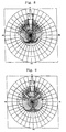
- FIG. 6 shows a graph which plots the radiation patterns of the antenna which utilizes metallic coating according to the results of the experiment.
- FIG. 7 shows a graph which plots the radiation patterns of the antenna which utilizes metallic coating according to the results of the experiment.
- FIG. 8 shows a graph which plots the radiation patterns of the antenna which utilizes metallic coating according to the results of the experiment.
- FIG. 9 shows a graph which plots the radiation patterns of the antenna which utilizes metallic coating according to the results of the experiment.
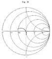
- FIG. 10 shows a graph which plots the variation of input impedance due to frequency change of the antenna which utilizes metallic coating.
- the manufacturing steps of the antenna which utilizes metallic coating according to the present invention comprises: a molding step S1 for molding the lower layer conductive panel 130, mid layer conductive panel 120 and upper layer conductive panel 110 after pouring synthetic resin into a molding fixture; a checking step S2 for checking the molding for any deformation, incomplete part and addition of foreign substances on the external body of the lower layer conductive panel 130, mid layer conductive panel 120 and upper layer conductive panel 110; a checking step S3 for checking the material analysis and chemical composition of the lower layer conductive panel 130, mid layer conductive panel 120 and upper layer conductive panel 110 after finishing the previous step; a drying step S4 for completely drying the lower layer conductive panel 130, mid layer conductive panel 120 and upper layer conductive panel 110 by putting them in a drier for a fixed amount of time; an etching step S5 (chemicals used: CrO 3 , H 2 SO 4 , Cr +3 ) for etching the surface in order to improve the degree of crystallization of the lower layer conductive panel 130,
- the deposition step S7 utilizes a non-electrolyte coating of a metallic substance on the face of the lower layer conductive panel 130, mid layer conductive panel 120 and upper layer conductive panel 110 or utilizes a spray gun.
- the effectcs of the antenna that uses a metallic coating and manufacturing method thereof according to the present invention are as follows.
- the metal molding for the lower layer conductive panel 130, mid layer conductive panel 120 and upper layer conductive panel 110 are produced and synthetic resin is poured into the metal molding and finally the lower layer conductive panel 130, mid layer conductive panel 120 and upper layer conductive panel 110 are formed.
- the molding of the lower layer conductive panel 130, mid layer conductive panel 120 and upper layer conductive panel 110 are checked first.
- the external body of the lower layer conductive panel 130, mid layer conductive panel 120 and upper layer conductive panel 110 are checked for any deformation, incomplete part and addition of foreign substances.
- a checking of material analysis and chemical composition of the lower layer conductive panel 130, mid layer conductive panel 120 and upper layer conductive panel 110 is carried out using a dedicated jig.
- the lower layer conductive panel 130, mid layer conductive panel 120 and upper layer conductive panel 110 are cleaned using cleaning Chlorine and dried. After the drying, a annealing process is carried out in order to increase the degree of crystallization of lower layer conductive panel 130, mid layer conductive panel 120 and upper layer conductive panel 110 and an etching is carried out in order to result a uniform surface.
- the lower layer conductive panel 130, mid layer conductive panel 120 and upper layer conductive panel 110 are cleaned and dried again.
- a thin metallic coating (Cu, H 2 SO 4 , CuSO 4 , 5H 2 O, H 3 BO 3 , SB-75, SB-70M, NISO 4 , EX, 6H 2 O, G1, G2, Chrome) is formed on the surface of the lower layer conductive panel 130, mid layer conductive panel 120 and upper layer conductive panel 110 using a non-electrolyte coating method.
- mid layer conductive panel 120 and upper layer conductive panel 110 After a metallic substance deposited on the surface of the lower layer conductive panel 130, mid layer conductive panel 120 and upper layer conductive panel 110 and dried for a fixed amount of time (6 min 10 sec - 7 min 10 sec) at an appropriate temperature (35°C - 43 °C). Then quality of deposition on the lower layer conductive panel 130, mid layer conductive panel 120 and upper layer conductive panel 110 is checked and a surface checking for adherence strength is carried out. The adherence strength is checked using a separate jig and the surface is checked by a microscope.
- Table 1 represents the measurements of antenna gains for a metal waveguide slot antenna and the antenna according to the present invention. As the measurements in Table 1 show, the gain value at each GHz band show a better result than the existing antenna made of a metallic substance.
- Table 1 Satellite communication frequency(GHz) Gain of metal antenna(dBi) Gain of antenna according to present invention(dBi) 10.70 31.12 31.15 11.70 31.48 31.51 12.27 31.50 31.52 12.75 31.56 3157
- the reception gain at 10.7 GHz for the metallic waveguide slot antenna is 31.12[dBi] whereas the reception gain for the antenna according to the present invention is 31.15[dBi].
- the corresponding radiation pattern is shown in FIG. 6.
- the reception gain at 11.7 GHz for the antenna according to the present invention is 31. 51[dBi] and the corresponding radiation pattern is shown in FIG. 7.
- the reception gain at 12.27 GHz for the antenna according to the present invention is 31. 52[dBi] and the corresponding radiation pattern is shown in FIG. 8.
- the reception gain at 12.57 GHz for the antenna according to the present invention is 31. 57[dBi] and the corresponding radiation pattern is shown in FIG. 9.
- the antenna gain difference between the metallic waveguide slot antenna and the antenna according to the present invention show that the latter has a slightly higher value.
- the antenna according to the present invention can be used for the purpose of communication or broadcasting depending on the design method. Also the performance is comparable or better than a metallic waveguide slot antenna.
- an antenna fixing apparatus or an easy to handle antenna can be manufactured.
- the metal coated synthetic resin antenna there is no limit in the shape of the antenna (circular, rectangular, hexagonal, octagonal, polygonal)
- the effect of the manufacturing method for the waveguide slot antenna according to the present invention can be utilized for a high power output antenna due to its small resistance and radiation loss. Also it can obtain an high gain value due to its small dielectric loss.
- the antenna can be manufactured by an assembly type of conducting panels, hence, its manufacturing is simple and miniaturization is easily achievable. It can easily be installed and portable resulting in a significant saving for installment.
- the antenna is made of synthetic resin, the degree of precision that can be achieved for manufacturing is superior.
Applications Claiming Priority (4)
| Application Number | Priority Date | Filing Date | Title |
|---|---|---|---|
| KR20010014477 | 2001-03-21 | ||
| KR20010049929 | 2001-08-20 | ||
| KR1020020013581A KR100399193B1 (en) | 2002-03-13 | 2002-03-13 | Waveguide slot antenna and manufacturing method thereof |
| EP02707304A EP1371112B1 (fr) | 2001-03-21 | 2002-03-20 | Antenne a fentes en guide d'ondes et procede de fabrication |
Related Parent Applications (1)
| Application Number | Title | Priority Date | Filing Date |
|---|---|---|---|
| EP02707304A Division EP1371112B1 (fr) | 2001-03-21 | 2002-03-20 | Antenne a fentes en guide d'ondes et procede de fabrication |
Publications (1)
| Publication Number | Publication Date |
|---|---|
| EP1753085A1 true EP1753085A1 (fr) | 2007-02-14 |
Family
ID=27350430
Family Applications (2)
| Application Number | Title | Priority Date | Filing Date |
|---|---|---|---|
| EP02707304A Expired - Lifetime EP1371112B1 (fr) | 2001-03-21 | 2002-03-20 | Antenne a fentes en guide d'ondes et procede de fabrication |
| EP06022044A Withdrawn EP1753085A1 (fr) | 2001-03-21 | 2002-03-20 | Antenne à fentes en guide d'ondes et procédé de fabrication |
Family Applications Before (1)
| Application Number | Title | Priority Date | Filing Date |
|---|---|---|---|
| EP02707304A Expired - Lifetime EP1371112B1 (fr) | 2001-03-21 | 2002-03-20 | Antenne a fentes en guide d'ondes et procede de fabrication |
Country Status (10)
| Country | Link |
|---|---|
| US (1) | US6861996B2 (fr) |
| EP (2) | EP1371112B1 (fr) |
| JP (2) | JP3874279B2 (fr) |
| CN (1) | CN1290226C (fr) |
| AT (1) | ATE361555T1 (fr) |
| CA (1) | CA2440508C (fr) |
| DE (1) | DE60219896T2 (fr) |
| ES (1) | ES2282390T3 (fr) |
| NZ (1) | NZ528252A (fr) |
| WO (1) | WO2002078125A1 (fr) |
Cited By (2)
| Publication number | Priority date | Publication date | Assignee | Title |
|---|---|---|---|---|
| DE102010003457A1 (de) * | 2010-03-30 | 2011-10-06 | Fraunhofer-Gesellschaft zur Förderung der angewandten Forschung e.V. | Leckwellenantenne |
| US8482361B2 (en) | 2008-03-25 | 2013-07-09 | Mitsubishi Electric Corporation | Waveguide power divider having coupling slots between stacked waveguide portions and method of manufacture |
Families Citing this family (54)
| Publication number | Priority date | Publication date | Assignee | Title |
|---|---|---|---|---|
| US7109939B2 (en) * | 2002-05-14 | 2006-09-19 | Hrl Laboratories, Llc | Wideband antenna array |
| US7391381B2 (en) * | 2004-01-07 | 2008-06-24 | Motia | Vehicle mounted satellite antenna system with in-motion tracking using beam forming |
| US6977621B2 (en) * | 2004-01-07 | 2005-12-20 | Motia, Inc. | Vehicle mounted satellite antenna system with inverted L-shaped waveguide |
| US7227508B2 (en) * | 2004-01-07 | 2007-06-05 | Motia Inc. | Vehicle mounted satellite antenna embedded within moonroof or sunroof |
| WO2005079158A2 (fr) * | 2004-02-23 | 2005-09-01 | Galtronics Ltd. | Antenne a faisceau conique a fentes transversales |
| US7205948B2 (en) * | 2005-05-24 | 2007-04-17 | Raytheon Company | Variable inclination array antenna |
| JP4394147B2 (ja) * | 2006-02-06 | 2010-01-06 | 三菱電機株式会社 | 高周波モジュール |
| CN101083359B (zh) * | 2007-07-10 | 2012-05-09 | 中国电子科技集团公司第五十四研究所 | 高增益双线极化或双圆极化波导阵列天线制造方法 |
| KR20090047015A (ko) * | 2007-11-07 | 2009-05-12 | 위월드 주식회사 | 개선된 원편파 수신용 도파관 슬롯 배열 안테나 |
| JP4959594B2 (ja) * | 2008-02-01 | 2012-06-27 | パナソニック株式会社 | エンドファイアアンテナ装置 |
| US20100238085A1 (en) * | 2009-03-23 | 2010-09-23 | Toyota Motor Engineering & Manufacturing North America, Inc. | Plastic waveguide slot array and method of manufacture |
| US8866686B1 (en) | 2009-03-25 | 2014-10-21 | Raytheon Company | Methods and apparatus for super-element phased array radiator |
| US8907842B1 (en) | 2009-03-25 | 2014-12-09 | Raytheon Company | Method and apparatus for attenuating a transmitted feedthrough signal |
| CN101615930B (zh) * | 2009-07-28 | 2013-01-02 | 华为技术有限公司 | 微波通信设备、适配器及通信系统 |
| DE102009055344A1 (de) * | 2009-12-29 | 2011-06-30 | Robert Bosch GmbH, 70469 | Antenne |
| JP5558943B2 (ja) * | 2010-07-06 | 2014-07-23 | 古野電気株式会社 | スロットアレイアンテナ及びレーダ装置 |
| CH704552A8 (de) | 2011-02-17 | 2012-10-15 | Huber+Suhner Ag | Gruppenantenne. |
| CN102255138A (zh) * | 2011-03-28 | 2011-11-23 | 李峰 | 圆极化波导平板阵列天线 |
| KR101405294B1 (ko) * | 2011-06-09 | 2014-06-11 | 위월드 주식회사 | 통신용 초광대역 듀얼선형편파 도파관 안테나 |
| CN102394376B (zh) * | 2011-07-12 | 2014-02-26 | 北京理工大学 | 毫米波圆极化一维和差车载通信天线 |
| RU2474019C1 (ru) * | 2011-07-12 | 2013-01-27 | Открытое акционерное общество Центральное конструкторское бюро аппаратостроения | Фазированная антенная решетка с электронным сканированием в одной плоскости |
| CN102394377B (zh) * | 2011-07-12 | 2013-12-25 | 北京理工大学 | 毫米波线极化车载扇形波束天线 |
| CN102437432B (zh) * | 2011-09-09 | 2014-01-15 | 陕西长岭电子科技有限责任公司 | 一种平板裂缝阵天线粘接加工方法 |
| US9160049B2 (en) | 2011-11-16 | 2015-10-13 | Commscope Technologies Llc | Antenna adapter |
| US8558746B2 (en) | 2011-11-16 | 2013-10-15 | Andrew Llc | Flat panel array antenna |
| US8866687B2 (en) * | 2011-11-16 | 2014-10-21 | Andrew Llc | Modular feed network |
| MX2015009202A (es) * | 2013-01-21 | 2015-12-01 | Nec Corp | Antena. |
| US9129954B2 (en) * | 2013-03-07 | 2015-09-08 | Advanced Semiconductor Engineering, Inc. | Semiconductor package including antenna layer and manufacturing method thereof |
| US9379446B1 (en) | 2013-05-01 | 2016-06-28 | Raytheon Company | Methods and apparatus for dual polarized super-element phased array radiator |
| CN103414027B (zh) * | 2013-07-18 | 2015-08-19 | 北京遥测技术研究所 | 一种宽频带单脉冲平板缝隙阵列天线 |
| CN103414030B (zh) * | 2013-07-18 | 2015-08-19 | 北京遥测技术研究所 | 一种宽频带低剖面平板缝隙阵列天线 |
| CN104716426A (zh) * | 2013-12-13 | 2015-06-17 | 华为技术有限公司 | 一种阵列天线 |
| US9472853B1 (en) | 2014-03-28 | 2016-10-18 | Google Inc. | Dual open-ended waveguide antenna for automotive radar |
| ES2746398T3 (es) * | 2014-05-12 | 2020-03-06 | Huawei Tech Co Ltd | Antena y dispositivo inalámbrico |
| US10281571B2 (en) | 2014-08-21 | 2019-05-07 | Raytheon Company | Phased array antenna using stacked beams in elevation and azimuth |
| KR102302466B1 (ko) * | 2014-11-11 | 2021-09-16 | 주식회사 케이엠더블유 | 도파관 슬롯 어레이 안테나 |
| CN104638374B (zh) * | 2014-12-24 | 2017-07-28 | 西安电子工程研究所 | 一种c/x双波段共口径波导缝隙阵列天线 |
| CA2980920C (fr) | 2015-03-25 | 2023-09-26 | King Abdulaziz City Of Science And Technology | Appareil et procedes pour radar a synthese d'ouverture avec formation de faisceau numerique |
| US9876282B1 (en) | 2015-04-02 | 2018-01-23 | Waymo Llc | Integrated lens for power and phase setting of DOEWG antenna arrays |
| WO2017044168A2 (fr) * | 2015-06-16 | 2017-03-16 | King Abdulaziz City Of Science And Technology | Ensemble antenne plane à réseau de phases efficace |
| US10033082B1 (en) * | 2015-08-05 | 2018-07-24 | Waymo Llc | PCB integrated waveguide terminations and load |
| CA3044806A1 (fr) | 2015-11-25 | 2017-06-01 | Urthecast Corp. | Appareil et procedes d'imagerie radar a synthese d'ouverture |
| JP6686820B2 (ja) * | 2016-03-17 | 2020-04-22 | 住友電気工業株式会社 | アンテナおよびレーダ |
| CN109314314B (zh) | 2016-06-29 | 2021-08-27 | 胡贝尔和茹纳股份公司 | 阵列天线 |
| WO2018086998A1 (fr) * | 2016-11-08 | 2018-05-17 | Robin Radar Facilities Bv | Réseau d'antennes guide d'ondes à fentes, procédé de fabrication d'un réseau d'antennes guide d'ondes à fentes, et module d'antenne radar comprenant des réseaux d'antennes guide d'ondes à fentes |
| JP6809702B2 (ja) * | 2016-11-10 | 2021-01-06 | 国立大学法人東京工業大学 | スロットアレーアンテナ |
| US11378682B2 (en) | 2017-05-23 | 2022-07-05 | Spacealpha Insights Corp. | Synthetic aperture radar imaging apparatus and methods for moving targets |
| EP3631504B8 (fr) | 2017-05-23 | 2023-08-16 | Spacealpha Insights Corp. | Appareil et procédés d'imagerie radar à synthèse d'ouverture |
| CN107342454B (zh) * | 2017-06-09 | 2020-02-21 | 宁波大学 | 一种波导缝隙阵列天线 |
| US11525910B2 (en) | 2017-11-22 | 2022-12-13 | Spacealpha Insights Corp. | Synthetic aperture radar apparatus and methods |
| CN110323551B (zh) * | 2018-03-30 | 2023-05-26 | 普罗斯通信技术(苏州)有限公司 | 一种贴片辐射单元 |
| CN109149126A (zh) * | 2018-08-30 | 2019-01-04 | 成都赛康宇通科技有限公司 | 相控阵天线缝隙波导层制备工艺 |
| CN111106432A (zh) * | 2018-10-26 | 2020-05-05 | 网易达科技(北京)有限公司 | 天线及信号处理装置 |
| CN111370856B (zh) * | 2020-03-23 | 2022-08-19 | 中天通信技术有限公司 | 一种波导缝隙天线的制备方法 |
Citations (3)
| Publication number | Priority date | Publication date | Assignee | Title |
|---|---|---|---|---|
| WO1991020109A1 (fr) * | 1990-06-14 | 1991-12-26 | Collins John Louis Frederick C | Antennes a micro-ondes |
| US6017628A (en) * | 1989-12-11 | 2000-01-25 | Alliant Defense Electronics Systems, Inc. | Metal-coated substrate articles responsive to electromagnetic radiation, and method of making and using the same |
| US6201508B1 (en) * | 1999-12-13 | 2001-03-13 | Space Systems/Loral, Inc. | Injection-molded phased array antenna system |
Family Cites Families (30)
| Publication number | Priority date | Publication date | Assignee | Title |
|---|---|---|---|---|
| US3950204A (en) * | 1972-09-29 | 1976-04-13 | Texas Instruments Incorporated | Low pressure, thin film bonding |
| JPS5775006A (en) * | 1980-10-29 | 1982-05-11 | Mitsubishi Electric Corp | Array antenna |
| JPS62141801A (ja) * | 1985-12-16 | 1987-06-25 | Nec Corp | 導波管回路 |
| JP2733472B2 (ja) * | 1988-02-19 | 1998-03-30 | 有限会社ラジアルアンテナ研究所 | 導波管スロット・アンテナ及びその製造方法並びに導波管の結合構造 |
| JPH0365805A (ja) * | 1989-08-03 | 1991-03-20 | Sumitomo Bakelite Co Ltd | 導波管アンテナ |
| JPH0376305A (ja) * | 1989-08-17 | 1991-04-02 | Sumitomo Bakelite Co Ltd | 導波管アンテナ |
| JPH04358405A (ja) * | 1991-06-05 | 1992-12-11 | Asahi Chem Ind Co Ltd | 導波管スロットアレーアンテナ |
| JPH053405A (ja) * | 1991-06-25 | 1993-01-08 | Asahi Chem Ind Co Ltd | 導波管結合構造 |
| SE469540B (sv) * | 1991-11-29 | 1993-07-19 | Ericsson Telefon Ab L M | Vaagledarantenn med slitsade haalrumsvaagledare |
| JPH06125207A (ja) * | 1992-10-12 | 1994-05-06 | Nec Corp | ミリ波帯導波路 |
| US5327150A (en) * | 1993-03-03 | 1994-07-05 | Hughes Aircraft Company | Phased array antenna for efficient radiation of microwave and thermal energy |
| KR960015570B1 (ko) * | 1993-05-13 | 1996-11-18 | 휴즈 에어크라프트 캄파니 | 성형 플라스틱 마이크로웨이브 안테나 |
| JPH0758519A (ja) * | 1993-08-19 | 1995-03-03 | Nec Eng Ltd | 分波器 |
| JPH07106847A (ja) * | 1993-10-07 | 1995-04-21 | Nippon Steel Corp | 漏れ波導波管スロットアレーアンテナ |
| SE510082C2 (sv) * | 1993-11-30 | 1999-04-19 | Saab Ericsson Space Ab | Vågledarantenn med tvärgående och längsgående slitsar |
| JP2713179B2 (ja) * | 1994-03-28 | 1998-02-16 | 日本電気株式会社 | 分波器 |
| KR960015570A (ko) | 1994-10-07 | 1996-05-22 | 이헌조 | 집적회로의 내부버스 모니터장치 |
| JP3569078B2 (ja) * | 1996-06-14 | 2004-09-22 | Dxアンテナ株式会社 | フェイズドアレイアンテナ用周波数変換器 |
| US6028562A (en) * | 1997-07-31 | 2000-02-22 | Ems Technologies, Inc. | Dual polarized slotted array antenna |
| US6201507B1 (en) * | 1998-04-09 | 2001-03-13 | Raytheon Company | Centered longitudinal shunt slot fed by a resonant offset ridge iris |
| SE513586C2 (sv) * | 1998-05-12 | 2000-10-02 | Ericsson Telefon Ab L M | Metod för framställning av en antennstruktur och antennstruktur framställd medelst nämnda metod |
| EP0966057A1 (fr) * | 1998-06-15 | 1999-12-22 | TRT Lucent Technologies (SA) | Atténuateur variable pour guide d'ondes rectangulaire |
| JP2000013135A (ja) * | 1998-06-22 | 2000-01-14 | Yagi Antenna Co Ltd | スロットアレイアンテナ |
| IT1303866B1 (it) * | 1998-11-25 | 2001-03-01 | Italtel Spa | Filtro disaccoppiante per rice-trasmittitori ad alta frequenzaautocompensato in temperatura |
| JP2000349538A (ja) * | 1999-06-04 | 2000-12-15 | Kobe Steel Ltd | 導波管アンテナ |
| JP2001044744A (ja) * | 1999-07-29 | 2001-02-16 | Kobe Steel Ltd | 導波管アンテナ |
| JP2001060807A (ja) * | 1999-08-20 | 2001-03-06 | Anritsu Corp | サーキュレータ及び該サーキュレータを用いたモジュール |
| JP2001156542A (ja) * | 1999-11-30 | 2001-06-08 | Kyocera Corp | 導波管スロットアレーアンテナ |
| EP1291966B1 (fr) * | 2000-04-18 | 2010-08-11 | Hitachi Chemical Company, Ltd. | Antenne planar de balayage de faisceau |
| JP4021150B2 (ja) * | 2001-01-29 | 2007-12-12 | 沖電気工業株式会社 | スロットアレーアンテナ |
-
2002
- 2002-03-20 CN CNB028057740A patent/CN1290226C/zh not_active Expired - Fee Related
- 2002-03-20 NZ NZ528252A patent/NZ528252A/en unknown
- 2002-03-20 ES ES02707304T patent/ES2282390T3/es not_active Expired - Lifetime
- 2002-03-20 US US10/469,764 patent/US6861996B2/en not_active Expired - Fee Related
- 2002-03-20 AT AT02707304T patent/ATE361555T1/de not_active IP Right Cessation
- 2002-03-20 EP EP02707304A patent/EP1371112B1/fr not_active Expired - Lifetime
- 2002-03-20 JP JP2002576053A patent/JP3874279B2/ja not_active Expired - Fee Related
- 2002-03-20 EP EP06022044A patent/EP1753085A1/fr not_active Withdrawn
- 2002-03-20 WO PCT/KR2002/000468 patent/WO2002078125A1/fr active IP Right Grant
- 2002-03-20 CA CA002440508A patent/CA2440508C/fr not_active Expired - Fee Related
- 2002-03-20 DE DE60219896T patent/DE60219896T2/de not_active Expired - Fee Related
-
2006
- 2006-08-30 JP JP2006233852A patent/JP2006352915A/ja active Pending
Patent Citations (3)
| Publication number | Priority date | Publication date | Assignee | Title |
|---|---|---|---|---|
| US6017628A (en) * | 1989-12-11 | 2000-01-25 | Alliant Defense Electronics Systems, Inc. | Metal-coated substrate articles responsive to electromagnetic radiation, and method of making and using the same |
| WO1991020109A1 (fr) * | 1990-06-14 | 1991-12-26 | Collins John Louis Frederick C | Antennes a micro-ondes |
| US6201508B1 (en) * | 1999-12-13 | 2001-03-13 | Space Systems/Loral, Inc. | Injection-molded phased array antenna system |
Cited By (4)
| Publication number | Priority date | Publication date | Assignee | Title |
|---|---|---|---|---|
| US8482361B2 (en) | 2008-03-25 | 2013-07-09 | Mitsubishi Electric Corporation | Waveguide power divider having coupling slots between stacked waveguide portions and method of manufacture |
| CN101978553B (zh) * | 2008-03-25 | 2013-07-31 | 三菱电机株式会社 | 波导管功率分配器及其制造方法 |
| DE102010003457A1 (de) * | 2010-03-30 | 2011-10-06 | Fraunhofer-Gesellschaft zur Förderung der angewandten Forschung e.V. | Leckwellenantenne |
| US8570238B2 (en) | 2010-03-30 | 2013-10-29 | Fraunhofer-Gesellschaft Zur Foerderung Der Angewandten Forschung E.V. | Leaky-wave antenna |
Also Published As
| Publication number | Publication date |
|---|---|
| CN1290226C (zh) | 2006-12-13 |
| ATE361555T1 (de) | 2007-05-15 |
| JP2006352915A (ja) | 2006-12-28 |
| WO2002078125A1 (fr) | 2002-10-03 |
| CA2440508A1 (fr) | 2002-10-03 |
| JP3874279B2 (ja) | 2007-01-31 |
| NZ528252A (en) | 2005-03-24 |
| EP1371112A1 (fr) | 2003-12-17 |
| EP1371112A4 (fr) | 2005-04-20 |
| CN1494751A (zh) | 2004-05-05 |
| CA2440508C (fr) | 2007-05-22 |
| DE60219896T2 (de) | 2008-01-17 |
| ES2282390T3 (es) | 2007-10-16 |
| US20040080463A1 (en) | 2004-04-29 |
| US6861996B2 (en) | 2005-03-01 |
| EP1371112B1 (fr) | 2007-05-02 |
| DE60219896D1 (de) | 2007-06-14 |
| JP2004526368A (ja) | 2004-08-26 |
Similar Documents
| Publication | Publication Date | Title |
|---|---|---|
| EP1371112B1 (fr) | Antenne a fentes en guide d'ondes et procede de fabrication | |
| TWI237924B (en) | Wideband antenna array | |
| KR101677521B1 (ko) | 고 이득 메타물질 안테나 소자 | |
| US5568159A (en) | Flared notch slot antenna | |
| CN113285237B (zh) | 一种宽带、高增益Fabry-Pérot谐振腔天线 | |
| CN104953293A (zh) | 一种基于c波段的圆极化喇叭天线 | |
| CN204947091U (zh) | 一种基于c波段的圆极化喇叭天线 | |
| Uchimura et al. | Novel circular polarized antenna array substrates for 60GHz-band | |
| JPH11251833A (ja) | マイクロストリップアンテナ素子およびマイクロストリップアレーアンテナ | |
| US7515013B2 (en) | Rectangular waveguide cavity launch | |
| Lomakin et al. | 3D printed helix antenna | |
| CN1897352A (zh) | 波导缝隙天线的制造方法 | |
| Esmaeili et al. | Coaxial-fed dual-layer SIW horn antenna with improved E-plane radiation pattern | |
| Sato et al. | Design of narrow-width Fermi antenna with circular radiation pattern | |
| CN116111334A (zh) | 一种新型车载毫米波雷达梳状天线 | |
| AU2002241365A1 (en) | Waveguide slot antenna and manufacturing method thereof | |
| KR100400656B1 (ko) | 금속제 코팅에 의한 안테나 제조방법 및 그 제품 | |
| CN114665283A (zh) | W波段大规模圆口径高效率siw缝隙阵列天线 | |
| CN110620293B (zh) | 一种基于六臂螺旋阵列结构的稀疏阵天线 | |
| US20050151694A1 (en) | Notched slot antenna | |
| Hassanien et al. | Miniaturized beam steerable system using rotman lens for mm wave applications at 60GHz | |
| CN215579071U (zh) | 一种采用近零超材料加载的siw喇叭天线 | |
| Khan et al. | Hybrid Thin Film Multilayer Antenna Automotive Radar at 77 GHz | |
| Cao et al. | Design of a Millimeter-wave Slotted Array Antenna with Miniaturized Dimension and Low Side-lobes | |
| KR20040071986A (ko) | 도파관 형태의 유전체 세라믹 필터 |
Legal Events
| Date | Code | Title | Description |
|---|---|---|---|
| PUAI | Public reference made under article 153(3) epc to a published international application that has entered the european phase |
Free format text: ORIGINAL CODE: 0009012 |
|
| 17P | Request for examination filed |
Effective date: 20061020 |
|
| AC | Divisional application: reference to earlier application |
Ref document number: 1371112 Country of ref document: EP Kind code of ref document: P |
|
| AK | Designated contracting states |
Kind code of ref document: A1 Designated state(s): AT BE CH CY DE DK ES FI FR GB GR IE IT LI LU MC NL PT SE TR |
|
| 17Q | First examination report despatched |
Effective date: 20070402 |
|
| AKX | Designation fees paid |
Designated state(s): AT BE CH CY DE DK ES FI FR GB GR IE IT LI LU MC NL PT SE TR |
|
| STAA | Information on the status of an ep patent application or granted ep patent |
Free format text: STATUS: THE APPLICATION IS DEEMED TO BE WITHDRAWN |
|
| 18D | Application deemed to be withdrawn |
Effective date: 20091222 |