EP1742364B1 - Tampon d'entrée amélioré pour circuits integrés CMOS - Google Patents
Tampon d'entrée amélioré pour circuits integrés CMOS Download PDFInfo
- Publication number
- EP1742364B1 EP1742364B1 EP06116225.1A EP06116225A EP1742364B1 EP 1742364 B1 EP1742364 B1 EP 1742364B1 EP 06116225 A EP06116225 A EP 06116225A EP 1742364 B1 EP1742364 B1 EP 1742364B1
- Authority
- EP
- European Patent Office
- Prior art keywords
- type fet
- gate
- output
- source
- voltage
- Prior art date
- Legal status (The legal status is an assumption and is not a legal conclusion. Google has not performed a legal analysis and makes no representation as to the accuracy of the status listed.)
- Active
Links
Images


Classifications
-
- H—ELECTRICITY
- H03—ELECTRONIC CIRCUITRY
- H03K—PULSE TECHNIQUE
- H03K19/00—Logic circuits, i.e. having at least two inputs acting on one output; Inverting circuits
- H03K19/003—Modifications for increasing the reliability for protection
- H03K19/00369—Modifications for compensating variations of temperature, supply voltage or other physical parameters
- H03K19/00384—Modifications for compensating variations of temperature, supply voltage or other physical parameters in field effect transistor circuits
-
- H—ELECTRICITY
- H03—ELECTRONIC CIRCUITRY
- H03K—PULSE TECHNIQUE
- H03K19/00—Logic circuits, i.e. having at least two inputs acting on one output; Inverting circuits
- H03K19/0175—Coupling arrangements; Interface arrangements
- H03K19/0185—Coupling arrangements; Interface arrangements using field effect transistors only
- H03K19/018507—Interface arrangements
- H03K19/018521—Interface arrangements of complementary type, e.g. CMOS
Definitions
- the instant invention relates to an improved input buffer for CMOS integrated circuits.
- Input buffers are a very important subsystem for various blocks on the Application Specific Integrated Circuits (ASICs).
- the input buffers are used as peripheral devices in a block for receiving data from other on-chip devices or external systems.
- the circuitry is also used for buffering the input to the block. Further, the circuitry is used for reducing the parasitic input capacitance of the system as the total input capacitance is reduced to the parasitic input capacitance of the input buffer.
- Simple input blocks comprise a chain of inverter stages or Schmitt trigger circuitry for input buffering and input capacitance reduction. In order to attain minimum specified noise tolerance, an input low voltage, VIL, and an input high voltage, VIH, switch levels are specified.
- modem input circuitry With increasing complexity of ASICs, simple buffering and capacitance reduction is not sufficient for modem input circuitry. These systems have to communicate with several other systems working at different voltages. Hence the modem ASIC input buffers must provide protection for the CMOS devices inside the systems during interaction with other local logic blocks or external systems.
- the device dimensions are continuously shrinking to sub-micron technology.
- Such sub-micron technology devices cannot tolerate high input voltage because of reliability issues due to gate oxide breakdown and punchthrough effect.
- the gate-oxide breakdown voltage and/or the punchthrough voltage between source and drain are the parameters used to define the maximum input voltage allowed between various nodes of a CMOS device. These devices can operate without experiencing stress due to gate oxide breakdown and punchthrough effects while the input transistor voltages
- Vtgl is defined as the input voltage of an inverter chain, which produces 0.5Vdd at the output for supply voltage Vdd.
- the toggle voltage Vtgl is used as switching level for the logic in the digital circuits and this value lies between VIH and VIL.
- the minimum of the difference between Vtgl and VIH and Vtgl and VIL is used to determine the noise margin for the input buffer.
- Vtgl must lie within the switching window of 0.2Vdd and the maximum noise margin is 0.1Vdd.
- the switching window is getting progressively smaller resulting in reduced noise margin. This is a cause of concern as the variation in the integrated circuit manufacturing process can introduce a shift in the input switching voltage level Vtgl and result in further reduction in the noise margin for the circuitry.
- Figure 1 is a schematic diagram of a simple 5V tolerant input buffer operating at 3.3V nominal supply voltage. All CMOS devices used in the input buffer are designed in 3.3V CMOS technology.
- IN is connected to the drain of MOSFET M1, which translates the input signal to a lower voltage at the input node of the buffer for safe operation.
- VDDS-VtM1 the threshold voltage Vt of transistor M1 is high (over 1 V) and the buffer input node voltage is comparatively low resulting in safe transistor operation.
- VtM1 low voltage CMOS devices (i.e. 2.5V) with a high supply voltage (i.e. 3.3V).
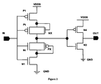
- FIG 2 is a schematic diagram of a process compensated input buffer presented in U. S 6,184,704 (Wang et al.). That patent describes an improved CMOS input buffer. This improvement reduces the switching level uncertainty range and thus increases the noise margin by compensating for the manufacturing process variations.
- Diode connected Px and Nx transistors are used as resistive compensation devices in the first stage of a multistage digital input buffer. Threshold loss is compensated for by Pt, Nt devices in parallel with Nx, Px devices, respectively.
- Pt, Nt devices in parallel with Nx, Px devices, respectively.
- this circuit does not provide independent control for process variation. Additionally compensation device is not on throughout the transition. Also, this structure cannot be used with low input voltage (i.e. 2.5V) with the input buffer having higher supply voltage (i.e. 3.3V).
- an input buffer which is capable of receiving a high input and supply voltage without experiencing degradation of gate oxide lifetime. Further there is need for an input buffer that provides good noise margin with process, temperature and voltage variation. Additionally, there is need for an input buffer that does not need increased process complexity in low voltage CMOS devices for protection against higher input and supply voltages.
- US-A-6,084,430 discloses a CMOS input buffer according to the preamble of claim 1 thereof.
- the object of the instant invention is to provide an improved input buffer for CMOS integrated circuits.
- Another object of the invention is to provide reduced process induced variation in voltage logic thresholds of a CMOS input buffer.
- Yet another object of the instant invention is to provide a method to design a robust CMOS input buffer using thin gate oxide transistors able to work with input voltage levels exceeding the tolerable voltage levels for the semiconductor devices used.
- Yet another object of the instant invention is to provide a means of shifting the voltage levels of input signals to tolerable limits for use by other circuits.
- Yet another object of the instant invention is to provide a high-speed input buffer with low power consumption.
- a further object of the instant invention is to provide immunity against noise in the input signal.
- an improved input buffer for CMOS integrated circuits comprising:
- the input voltage limiting circuit of the input buffer of the instant invention comprises:
- the objects have been achieved by providing a controlled parallel path of N-type for charging and P-type for discharging in the first inverter stage of a multistage digital input buffer.
- process variation refers to the drive ability of PMOS and NMOS devices. It is particularly troublesome when the NMOS devices have high drive ability and PMOS have low drive ability or when the PMOS devices have high drive ability and NMOS have low drive ability.
- the first case is referred as NSPF (NMOS slow PMOS fast) and the opposite case is referred as NFPS (NMOS fast PMOS slow).
- the input limiting circuit protects the transistors in the parallely connected inverter stage against high input voltage.
- the current invention relates to a high voltage tolerant input buffer using sub-micron CMOS technology.
- the invention provides additional input voltage limiting circuit resulting in a high voltage (3.3V or 5V) tolerant input buffer with low voltage tolerant CMOS devices. This improvement also reduces the switching level uncertainty due to the manufacturing process variations by adding compensation devices and thus increases the noise margin.
- the hysteresis characteristic produced by the circuit has reduced effect of manufacturing process variation.
- the circuit can be easily interfaced to other blocks and safely operates in conjunction with relatively high voltage CMOS technology circuitry while achieving the high-speed advantage of thin gate oxide. Low power consumption is achieved by avoiding any possibility of DC current flow in the circuitry.
- Figure 3 illustrates a schematic diagram of a proposed multistage input buffer.
- the instant invention is divided into two sections based on their operation.
- Section 1 is the proposed input voltage limiting circuit, which protects the input transistors in Section 2.
- Section 2 is a multistage input buffering circuitry where first stage is a modified CMOS inverter stage. The first inverter stage is coupled to a buffer stage to produce a delayed output.
- the preferred embodiment of the invention discussed herein relates to an input circuitry with two inverter stages. Furthermore for describing the functionality of the circuit nominal values for supply and reference voltages, and input signal level are taken in one of its embodiment.
- the voltage supply VDDS is 3.3V, and all devices are in low voltage (2.5V) CMOS technology and can operate without experiencing stress while the input transistor voltages
- the first inverter stage is modified to provide compensation for manufacturing process variations and simultaneously protect the input transistors from supply voltage stress.
- the second inverter stage is used to provide buffering of the signal output from the first inverter stage.
- the input voltage limiting circuit in Section 1 comprises NMOS transistors N7, N8, N9, N10 and N11, PMOS transistors P7, P8, P9, P10 and P11, and two inverters INV.
- IN is the input signal which varies between (0 - 3.6V) and is connected to node A and B through N7 and P7 respectively.
- the gate node K of N7 is connected to the coupled source node of P8 and P9 and the drain nodes of P8 and P9 are connected to VH and VDDS respectively.
- the gate nodes G and F of P8 and P9 are controlled by N10, P10 and INV.
- N10 and P10 are series connected to form an inverter stage with B and A connected at the gate nodes of P10 and N10 respectively.
- the source node of N10 is connected to the ground and the drain node of P10 is connected to VH.
- the output signal at the common node F between N10 and P10 is fed to an inverter INV with output node G.
- the gate node J of P7 is connected to the coupled source node of N8 and N9 and the drain nodes of N8 and N9 are connected to the VL and GND respectively.
- the gate nodes I and H of N8 and N9 are controlled by N11, P11 and INV.
- N11 and P11 are series connected to form an inverter stage with node B and A connected at the gate nodes of P11 and N11 respectively.
- the source node of N11 is connected to the ground and the drain node of P11 is connected to VH.
- the output signal at common node H between P11 and N11 is fed to an inverter INV with output node I.
- the modified inverter stage in Section 2 comprises NMOS transistors N1, N2, N3, N4, and NX, and PMOS transistors P1, P2, P3, P4, and PX.
- the first inverter stage of the input buffering circuitry (Section 2) has P1 and P2 connected in series to form a pull-up network and N1 and N2 connected in series to form a pull-down network. While the gate nodes of P2 and N2 are connected to VL and VH reference voltages respectively, the gate nodes of P1 and N1 are connected to node B and node A respectively.
- the output of the first inverter stage is the common node E between P2 and N2.
- a parallel path comprising P3, P4 and NX connected in series and N3, N4 and PX connected in series is used to form pull-up and pull-down networks, respectively.
- the gate node of NX is connected to the common node C between P1 and P2, and the gate nodes of P3 and P4 are connected to B and VL respectively.
- the gate node of PX is connected to the common node D between N2 and N1, and gate nodes of N3 and N4 are connected to A and VH respectively. Further common node between NX and PX is coupled to the output node E of the first inverter stage.
- Second inverter stage in the input buffering circuitry consists N5 and P5 connected in series to form a conventional inverter with the output signal of first inverter stage connected to the common gate node of N5 and P5.
- N5 and P5 are not stressed by the input and supply voltages, as the stress time is minimal due to the steep rise time of signal at E and fast clock operations
- the input voltage limiting circuit is used to protect the input transistors P1, P2, N1, N2, P3, N3 of the input buffering circuitry from stress by preventing
- VDDS-vtN7 the maximum value at A is (VDDS-vtN7) which is less than VH so N1, N2 and N3 are safe from stress. P7 is also not stressed in the process. H is at logic low and I is at logic high, so VL is applied to the gate node of P7 through N8 and hence P7 is not stressed either. Similarly, when IN is at logic low, H is at logic high and I is at logic low, so GND is applied at the gate node of P7 through N9.
- the input voltage limiting circuit passes signal IN unaltered to node A and node B while IN is in the range of
- the signal at node A is clamped at (VDDS-VtN7) to protect N1, N2, N3 and N7.
- the signal at node B is clamped at
- the switching threshold for inverter with N10 and P10 is kept slightly more than VL while that of inverter with N11 and P11 is kept slightly less than VH in order to insure the voltages at A and B follow IN in transition of signal at IN.
- the switching threshold voltages are kept at levels so input transition should not result in stress on N7 and P7.
- the initial voltages at J and K are VL and VDDS respectively.
- the voltage at J changes from VL to GND and the voltage at B follows the input at IN.
- the transition of J at this point also ensures the unstressed operation of device P7.
- the initial voltages at J and K are at GND and VH respectively.
- the voltage at K must change from VH to VDDS in order for voltage at A to follow input at IN.
- the first inverter stage is modified to provide device protection as well as reduced power consumption.
- the parallel path in the first inverter stage is used to reduce the effects of manufacturing process variations and thus increase the noise margins.
- Output node E of the first inverter stage swings from 0 to 3.3 volt (up to 3.6 volt in worst case) as it is directly connected to 3.3V power supply.
- V GB the gate to bulk voltage
- P2 and N2 are 2.6 volt and 2.5V respectively.
- P2 and N2 are also used to control reference signals at node C and node D connected to the compensation devices PX and NX in the parallel path.
- the parallel path with pull-up network of P3, P4, and NX and the pull-down network of N3, N4, and PX is inserted into the first inverter stage for compensating for manufacturing process variations.
- PX is connected as a compensation device along with NMOS devices in the pull-down path of the parallel path and NX is connected as a compensation device along with the PMOS devices in the pull-up path.
- PX and NX are used to decrease/increase the drive ability of the pull-up/down network in the inverter stage.
- P3, N3 transistors are used in the parallel pull-up and pull-down path to avoid the static current path through NX and PX respectively. Similar to P2 and N2, P4 and N4 with their gate nodes connected to VL and VH respectively are used in cascade with P3 and N3 to protect P3 and N3 from voltage stress.
- NMOS and PMOS devices are both present in pull-down and pull-up networks
- PX and NX greatly reduces the switching uncertainty range of the buffer throughout manufacturing process variation especially in cross corners (NSPF or NFPS).
- a second inverter stage is used to provide buffering of the signal coming from the first inverter stage. Also, as the added compensating devices work in the forward path in the input buffer, the proposed circuit is suitable for high-speed operation.
- Figure 5 illustrates the effect of process variation on the transfer curve of digital input buffer without compensation.
- the figure illustrates three transfer curves signifying a typical (normal) case, NSPF case and NFPS case.
- E is the voltage output of the first inverter stage of the input buffering stage and VIN is voltage input to the input buffer.
- Vtgl (T) is the switching voltage level for typical NMOS and PMOS process.
- Vtgl (NSPF) and Vtgl (NFPS) are the switching voltage levels for NMOS slow PMOS fast and NMOS fast and PMOS slow cases.
- the NSPF and NFPS transfer curves are shifted with respect to the typical case.
- the output may vary in the range of Vtgl(NSPF) and Vtgl(NFPS) in an uncompensated input buffer.
- Figure 6 illustrates the transfer curves of the first inverter stage of the input buffer in the instant invention.
- E is the voltage output of the first stage of the first inverter stage in input buffering stage and VIN is the voltage input to the input buffer.
- Three transfer curves of Typical, NSPF and PSNF are shown and the triggering voltages (Vtgl (NSPF) and Vtgl (NFPS)) are compared with respect to the uncompensated case.
- Addition of compensation devices reduces the gain of the transfer characteristic, making it more controllable during the transition period, as the devices NX, and PX begin to conduct whenever there gate to source voltage is greater than VtNX or
- pull-up and pull-down path of proposed circuit contain both NMOS and PMOS in their parallel path, the manufacturing process variation in one is compensated by the other, causing less deviation of triggering point at cross corners.
- Figure 7 illustrates the internal node voltages of the first inverter stage of Section 2, where VIN varies from Zero to VDDS.
- the controlling gate voltages C and D of NX and PX vary linearly, and precisely control the transfer characteristic of node E throughout the transition range. It also shows the node voltages A and B as the input voltage limiting circuit output clamped to allow stress free operation of Section 2.
- FIG. 4 illustrates another embodiment of the present invention using the Schmitt trigger in the proposed process compensated input buffer.
- P12 and N12 are added to the input buffer in feedback path with the output of the input buffer OUT connected to the gates of PMOS P12 and NMOS N12.
- the devices P12 and N12 are connected in series to form an inverter with output connected to E. Hence the output OUT is inverted and fed back to the second inverter stage resulting in reduction of noise.
Claims (10)
- Tampon d'entrée amélioré pour des circuits intégrés CMOS, comprenant :- des dispositifs de commutation à faible tension ;- une paire de tensions de référence, une haute et une basse, générées de façon interne (VH, VL), qui restent dans les limites de tension nominale des dispositifs de commutation à faible tension ;- un circuit limiteur de tension d'entrée (N7-N11, P7-P11, INV) qui utilise les tensions de référence pour limiter une entrée (IN) vers les dispositifs de commutation à faible tension ;caractérisé en ce que :- le tampon d'entrée comprend une pluralité d'inverseurs connectés en parallèle comprenant :et en ce que- une cascade (N2, N4, P2, P4) desdits dispositifs de commutation à faible tension polarisés en utilisant les tensions de référence pour limiter une contrainte de tension d'alimentation (VDDS), et- des moyens de compensation pour réduire les effets des variations de procédé de fabrication, couplés à des sorties (A, B) du circuit limiteur de tension d'entrée,
le circuit limiteur de tension d'entrée comprend :- un premier générateur de sortie (N7, P8, P9) recevant un premier signal de commande (F) et son signal complémentaire (G) pour brider ladite entrée et générer une première sortie (A) ;- un deuxième générateur de sortie (P7, N8, N9) recevant un deuxième signal de commande (H) et son signal complémentaire (I) pour brider ladite entrée et générer la deuxième sortie (B) ; et- un générateur de signaux de commande (N10, P10, N11, P11, INV) recevant les première et deuxième sorties pour générer les premier et deuxième signaux de commande et leurs signaux complémentaires. - Tampon d'entrée amélioré pour des circuits intégrés CMOS selon la revendication 1, dans lequel le premier générateur de sortie comprend :- un premier FET de type N (N7) connecté à ladite entrée au niveau du drain pour générer la première sortie au niveau de la source ;- un premier FET de type P (P9) connecté à une tension d'alimentation (VDDS) au niveau de la source et connecté au premier signal de commande (F) au niveau de la grille ;- un deuxième FET de type P (P8) connecté à la tension de référence haute au niveau de la source et connecté au signal complémentaire (G) du premier signal de commande au niveau de la grille ; et- une connexion entre les drains couplés du premier FET de type P et du deuxième FET de type P et la grille (K) du premier FET de type N.
- Tampon d'entrée amélioré pour des circuits intégrés CMOS selon la revendication 1 ou 2, dans lequel le deuxième générateur de sortie comprend :- un troisième FET de type P (P7) connecté à la tension d'entrée (IN) au niveau du drain pour générer la deuxième sortie (B) au niveau de la source ;- un deuxième FET de type N (N9) connecté à une masse (GND) au niveau de la source et connecté au deuxième signal de commande (H) au niveau de la grille ;- un troisième FET de type N (N8) connecté à la tension de référence basse (VL) au niveau de la source et connecté au signal complémentaire (I) du deuxième signal de commande (H) au niveau de la grille ; et- une connexion entre les drains couplés du deuxième FET de type N et du troisième FET de type N et la grille (J) du troisième FET de type P.
- Tampon d'entrée amélioré pour des circuits intégrés CMOS selon la revendication 1, 2 ou 3, dans lequel le générateur de signaux de commande comprend :- un quatrième FET de type N (N10) connecté à la première sortie (A) au niveau de la grille et connecté à la masse au niveau de la source ;- un quatrième FET de type P (P10) connecté à la deuxième sortie (B) au niveau de la grille et connecté à la tension d'alimentation au niveau de la source ;- un premier inverseur (INV) recevant le premier signal de commande (F) à partir d'un noeud couplé entre le quatrième FET de type P et le quatrième FET de type N ;- un cinquième FET de type N (N11) connecté à la première sortie (A) au niveau de la grille et connecté à la masse au niveau de la source ;- un cinquième FET de type P (P11) connecté à la deuxième sortie (B) au niveau de la grille et connecté à la tension d'alimentation au niveau de la source ; etun deuxième inverseur (INV) recevant le deuxième signal de commande à partir d'un noeud couplé entre le cinquième FET de type P et le cinquième FET de type N.
- Tampon d'entrée amélioré pour des circuits intégrés CMOS selon l'une quelconque des revendications précédentes, dans lequel l'inverseur connecté en parallèle comprend :- un sixième FET de type P (P1) connecté à la tension d'alimentation (VDDS) au niveau de la source et connecté à la deuxième sortie (B) au niveau de la grille ;- un premier FET de type P résistif (P2) connecté à la source du sixième FET de type P au niveau de la source et connecté à la tension de référence basse (VL) au niveau de la grille ;- un premier FET de type N résistif (N2) connecté au drain du premier FET de type P résistif au niveau du drain et connecté à la tension de référence haute (VH) au niveau de la grille ;- un sixième FET de type N (N1) connecté à la masse au niveau de la source et connecté à la première sortie (A) au niveau de la grille ;- un septième FET de type P (P3) connecté à la tension d'alimentation (VDDS) au niveau de la source et connecté à la deuxième sortie (B) au niveau de la grille ;- un deuxième FET de type P résistif (P4) connecté au drain (M) du septième FET de type P (P3) au niveau de la source et connecté à la tension de référence basse (VL) au niveau de la grille ;- un FET de type N de compensation (NX) connecté au drain (L) du deuxième FET de type P résistif (P4) au niveau du drain et connecté à un noeud commun (C) entre le sixième FET de type P (P1) et le premier FET de type P résistif (P2) au niveau de la grille ;- un FET de type P de compensation (PX) connecté à la source du FET de type N de compensation au niveau de la source et connecté à un noeud commun (D) entre le sixième FET de type N (N1) et le premier FET de type N résistif (N2) au niveau de la grille ;- un deuxième FET de type N résistif (N4) connecté à la source du FET de type P de compensation au niveau du drain (K) et connecté à la tension de référence haute (VH) au niveau de la grille ;- un septième FET de type N (N3) connecté à la masse (GND) au niveau de la source et connecté à la source (J) du deuxième FET de type N résistif (N4) au niveau du drain ;- une connexion entre la première sortie (A) et la grille du septième FET de type N (N3) ; et- une connexion entre un noeud commun (E) entre les premiers FET résistifs de type N et de type P et un noeud commun entre les FET de compensation pour générer une sortie de l'inverseur connecté en parallèle.
- Tampon d'entrée amélioré pour des circuits intégrés CMOS selon l'une quelconque des revendications précédentes, dans lequel les dispositifs de commutation sont des dispositifs MOSFET.
- Tampon d'entrée amélioré pour des circuits intégrés CMOS selon la revendication 5 ou 6, dans leur dépendance de la revendication 5, dans lequel les moyens de compensation comprennent le FET de type P de compensation (PX) et le FET de type N de compensation (NX) pour réduire les effets des variations de procédé de fabrication.
- Tampon d'entrée amélioré pour des circuits intégrés CMOS selon l'une quelconque des revendications précédentes, dans lequel les FET sont des dispositifs MOSFET.
- Tampon d'entrée amélioré pour des circuits intégrés CMOS selon l'une quelconque des revendications précédentes, dans lequel la sortie de l'inverseur connecté en parallèle est connectée à un étage tampon (N5, P5), pour maintenir une sortie (OUT) de l'étage tampon.
- Tampon d'entrée amélioré pour des circuits intégrés CMOS selon l'une quelconque des revendications précédentes, dans lequel la sortie de l'étage tampon est renvoyée vers la sortie de l'inverseur connecté en parallèle par l'intermédiaire d'un étage inverseur additionnel (N12, P12) pour former un étage tampon Trigger de Schmitt pour augmenter l'immunité au bruit.
Applications Claiming Priority (1)
| Application Number | Priority Date | Filing Date | Title |
|---|---|---|---|
| IN1688DE2005 | 2005-06-30 |
Publications (3)
| Publication Number | Publication Date |
|---|---|
| EP1742364A2 EP1742364A2 (fr) | 2007-01-10 |
| EP1742364A3 EP1742364A3 (fr) | 2008-12-31 |
| EP1742364B1 true EP1742364B1 (fr) | 2014-01-22 |
Family
ID=37092358
Family Applications (1)
| Application Number | Title | Priority Date | Filing Date |
|---|---|---|---|
| EP06116225.1A Active EP1742364B1 (fr) | 2005-06-30 | 2006-06-28 | Tampon d'entrée amélioré pour circuits integrés CMOS |
Country Status (2)
| Country | Link |
|---|---|
| US (1) | US7495483B2 (fr) |
| EP (1) | EP1742364B1 (fr) |
Families Citing this family (22)
| Publication number | Priority date | Publication date | Assignee | Title |
|---|---|---|---|---|
| JP4579027B2 (ja) * | 2005-03-29 | 2010-11-10 | 株式会社日出ハイテック | 負荷駆動回路 |
| US8610470B2 (en) * | 2008-12-10 | 2013-12-17 | Seiko Epson Corporation | Inverter circuit |
| GB2469636B8 (en) * | 2009-04-20 | 2017-08-02 | Advanced Risc Mach Ltd | Protecting lower voltage domain devices during operation in a higher voltage domain |
| JP2012080523A (ja) * | 2010-09-10 | 2012-04-19 | Renesas Electronics Corp | 制御電圧生成回路、定電流源回路及びそれらを有する遅延回路、論理回路 |
| TWI463600B (zh) | 2011-03-02 | 2014-12-01 | Global Unichip Corp | 二級式後端驅動器 |
| US8953267B2 (en) * | 2011-11-01 | 2015-02-10 | Lsi Corporation | Digital input detector and associated adaptive power supply |
| US8421501B1 (en) * | 2011-12-07 | 2013-04-16 | Arm Limited | Digital data handling in a circuit powered in a high voltage domain and formed from devices designed for operation in a lower voltage domain |
| US8610488B2 (en) * | 2012-01-12 | 2013-12-17 | Taiwan Semiconductor Manufacturing Co., Ltd. | 3X input voltage tolerant device and circuit |
| US9842066B2 (en) * | 2012-05-31 | 2017-12-12 | Nxp Usa, Inc. | Integrated circuit comprising an IO buffer driver and method therefor |
| KR101993192B1 (ko) | 2012-10-04 | 2019-06-27 | 삼성전자주식회사 | 다중 전압 입력 버퍼 |
| US8975929B2 (en) | 2013-06-20 | 2015-03-10 | Stmicroelectronics International N.V. | High voltage tolerant input buffer |
| KR20150006693A (ko) | 2013-07-09 | 2015-01-19 | 삼성전자주식회사 | 입력 버퍼의 프로세스 변화 보상 회로 및 이의 동작 방법 |
| KR102242582B1 (ko) * | 2014-10-10 | 2021-04-22 | 삼성전자주식회사 | 수신 회로 및 그것의 신호 수신 방법 |
| US9407243B1 (en) * | 2015-06-29 | 2016-08-02 | Global Unichip Corporation | Receiver circuit |
| US9735763B1 (en) | 2016-03-28 | 2017-08-15 | Qualcomm Incorporated | High voltage input receiver using low-voltage devices |
| KR102311490B1 (ko) * | 2017-05-26 | 2021-10-13 | 에스케이하이닉스 주식회사 | 입력 버퍼 회로를 포함하는 메모리 장치 및 메모리 시스템 |
| TWI654842B (zh) * | 2017-10-20 | 2019-03-21 | 立積電子股份有限公司 | 反相器 |
| US10700683B1 (en) | 2018-08-28 | 2020-06-30 | Qualcomm Incorporated | Dynamic power supply shifting |
| CN109274365A (zh) * | 2018-12-10 | 2019-01-25 | 上海艾为电子技术股份有限公司 | 输入缓冲器 |
| CN217445335U (zh) | 2020-11-10 | 2022-09-16 | 美商新思科技有限公司 | 输入缓冲器电路 |
| CN112468122B (zh) * | 2020-12-04 | 2023-08-18 | 哈尔滨工业大学 | 可配置延迟电路及延时配置方法 |
| WO2023196653A1 (fr) * | 2022-04-07 | 2023-10-12 | Sehat Sutardja | Tampon tolérant au bruit |
Family Cites Families (13)
| Publication number | Priority date | Publication date | Assignee | Title |
|---|---|---|---|---|
| JPH01286619A (ja) * | 1988-05-13 | 1989-11-17 | Nec Corp | 入力回路 |
| KR910009810B1 (ko) * | 1989-05-27 | 1991-11-30 | 삼성전자 주식회사 | Cmos 입력 버퍼 회로 |
| US5465054A (en) * | 1994-04-08 | 1995-11-07 | Vivid Semiconductor, Inc. | High voltage CMOS logic using low voltage CMOS process |
| KR100226486B1 (ko) * | 1996-12-21 | 1999-10-15 | 김영환 | 고출력 전압 생성용 반도체 회로 |
| US6023174A (en) * | 1997-07-11 | 2000-02-08 | Vanguard International Semiconductor Corporation | Adjustable, full CMOS input buffer for TTL, CMOS, or low swing input protocols |
| US6084430A (en) * | 1997-12-31 | 2000-07-04 | Intel Corporation | Input buffer for a mixed voltage environment |
| WO1999063668A1 (fr) * | 1998-06-04 | 1999-12-09 | Infineon Technologies Ag | Porte logique |
| US6147540A (en) * | 1998-08-31 | 2000-11-14 | Motorola Inc. | High voltage input buffer made by a low voltage process and having a self-adjusting trigger point |
| US6184704B1 (en) * | 1999-02-08 | 2001-02-06 | Tritech Microelectronics | Design method for compensation of process variation in CMOS digital input circuits |
| US6236236B1 (en) * | 1999-06-02 | 2001-05-22 | National Semiconductor Corporation | 2.5 volt input/output buffer circuit tolerant to 3.3 and 5 volts |
| US6784717B1 (en) * | 2002-08-28 | 2004-08-31 | Cypress Semiconductor Corporation | Input buffer system using low voltage transistors |
| US6784700B1 (en) * | 2002-09-03 | 2004-08-31 | Cypress Semiconductor Corporation | Input buffer circuit |
| US7164305B2 (en) * | 2004-06-08 | 2007-01-16 | Stmicroelectronics Pvt. Ltd. | High-voltage tolerant input buffer circuit |
-
2006
- 2006-06-27 US US11/475,846 patent/US7495483B2/en active Active
- 2006-06-28 EP EP06116225.1A patent/EP1742364B1/fr active Active
Also Published As
| Publication number | Publication date |
|---|---|
| US7495483B2 (en) | 2009-02-24 |
| EP1742364A2 (fr) | 2007-01-10 |
| EP1742364A3 (fr) | 2008-12-31 |
| US20070057703A1 (en) | 2007-03-15 |
Similar Documents
| Publication | Publication Date | Title |
|---|---|---|
| EP1742364B1 (fr) | Tampon d'entrée amélioré pour circuits integrés CMOS | |
| US5969542A (en) | High speed gate oxide protected level shifter | |
| US7183817B2 (en) | High speed output buffer with AC-coupled level shift and DC level detection and correction | |
| US6963226B2 (en) | Low-to-high level shifter | |
| US5973534A (en) | Dynamic bias circuit for driving low voltage I/O transistors | |
| US7164305B2 (en) | High-voltage tolerant input buffer circuit | |
| US8482329B2 (en) | High voltage input receiver with hysteresis using low voltage transistors | |
| US8253445B2 (en) | Output circuit having pre-emphasis function | |
| US9525421B2 (en) | High speed low voltage hybrid output driver for FPGA I/O circuits | |
| US7173472B2 (en) | Input buffer structure with single gate oxide | |
| US9780790B2 (en) | High speed level shifter circuit | |
| US20050127953A1 (en) | 5 Volt tolerant IO scheme using low-voltage devices | |
| US9374093B2 (en) | Capacitively coupled input buffer | |
| JP6065737B2 (ja) | 出力回路および電圧信号出力方法 | |
| US6392449B1 (en) | High-speed low-power low-offset hybrid comparator | |
| US9660651B2 (en) | Level shift circuit | |
| US7821327B2 (en) | High voltage input receiver using low voltage transistors | |
| KR100266628B1 (ko) | 입력버퍼 회로 | |
| US7999573B2 (en) | Low-voltage-to-high-voltage level converter for digital signals and related integrated circuit, system, and method | |
| US10447269B1 (en) | Level shifter | |
| US20070279091A1 (en) | Digital Voltage Level Shifter | |
| US6184704B1 (en) | Design method for compensation of process variation in CMOS digital input circuits | |
| US20070063738A1 (en) | CMOS logic circuitry | |
| US10911047B1 (en) | Level shifter with auto voltage-bias reliability protection | |
| KR20100133610A (ko) | 전압 레벨 시프터 |
Legal Events
| Date | Code | Title | Description |
|---|---|---|---|
| PUAI | Public reference made under article 153(3) epc to a published international application that has entered the european phase |
Free format text: ORIGINAL CODE: 0009012 |
|
| AK | Designated contracting states |
Kind code of ref document: A2 Designated state(s): AT BE BG CH CY CZ DE DK EE ES FI FR GB GR HU IE IS IT LI LT LU LV MC NL PL PT RO SE SI SK TR |
|
| AX | Request for extension of the european patent |
Extension state: AL BA HR MK YU |
|
| PUAL | Search report despatched |
Free format text: ORIGINAL CODE: 0009013 |
|
| AK | Designated contracting states |
Kind code of ref document: A3 Designated state(s): AT BE BG CH CY CZ DE DK EE ES FI FR GB GR HU IE IS IT LI LT LU LV MC NL PL PT RO SE SI SK TR |
|
| AX | Request for extension of the european patent |
Extension state: AL BA HR MK RS |
|
| 17P | Request for examination filed |
Effective date: 20090629 |
|
| 17Q | First examination report despatched |
Effective date: 20090729 |
|
| AKX | Designation fees paid |
Designated state(s): FR IT |
|
| REG | Reference to a national code |
Ref country code: DE Ref legal event code: 8566 |
|
| GRAP | Despatch of communication of intention to grant a patent |
Free format text: ORIGINAL CODE: EPIDOSNIGR1 |
|
| INTG | Intention to grant announced |
Effective date: 20130709 |
|
| GRAS | Grant fee paid |
Free format text: ORIGINAL CODE: EPIDOSNIGR3 |
|
| GRAA | (expected) grant |
Free format text: ORIGINAL CODE: 0009210 |
|
| RAP1 | Party data changed (applicant data changed or rights of an application transferred) |
Owner name: STMICROELECTRONICS INTERNATIONAL NV |
|
| AK | Designated contracting states |
Kind code of ref document: B1 Designated state(s): FR IT |
|
| PLBE | No opposition filed within time limit |
Free format text: ORIGINAL CODE: 0009261 |
|
| STAA | Information on the status of an ep patent application or granted ep patent |
Free format text: STATUS: NO OPPOSITION FILED WITHIN TIME LIMIT |
|
| 26N | No opposition filed |
Effective date: 20141023 |
|
| REG | Reference to a national code |
Ref country code: FR Ref legal event code: PLFP Year of fee payment: 11 |
|
| REG | Reference to a national code |
Ref country code: FR Ref legal event code: PLFP Year of fee payment: 12 |
|
| REG | Reference to a national code |
Ref country code: FR Ref legal event code: PLFP Year of fee payment: 13 |
|
| PGFP | Annual fee paid to national office [announced via postgrant information from national office to epo] |
Ref country code: IT Payment date: 20230523 Year of fee payment: 18 Ref country code: FR Payment date: 20230523 Year of fee payment: 18 |