EP1730506B1 - Integrierter elektronischer sensor - Google Patents
Integrierter elektronischer sensor Download PDFInfo
- Publication number
- EP1730506B1 EP1730506B1 EP05718823.7A EP05718823A EP1730506B1 EP 1730506 B1 EP1730506 B1 EP 1730506B1 EP 05718823 A EP05718823 A EP 05718823A EP 1730506 B1 EP1730506 B1 EP 1730506B1
- Authority
- EP
- European Patent Office
- Prior art keywords
- capacitive sensor
- sensor device
- integrated capacitive
- electrodes
- interconnect
- Prior art date
- Legal status (The legal status is an assumption and is not a legal conclusion. Google has not performed a legal analysis and makes no representation as to the accuracy of the status listed.)
- Not-in-force
Links
- 238000000034 method Methods 0.000 claims description 25
- 238000002161 passivation Methods 0.000 claims description 25
- 239000003990 capacitor Substances 0.000 claims description 21
- 239000000758 substrate Substances 0.000 claims description 17
- VYPSYNLAJGMNEJ-UHFFFAOYSA-N Silicium dioxide Chemical compound O=[Si]=O VYPSYNLAJGMNEJ-UHFFFAOYSA-N 0.000 claims description 16
- 238000012545 processing Methods 0.000 claims description 16
- 238000000151 deposition Methods 0.000 claims description 15
- 229910052710 silicon Inorganic materials 0.000 claims description 10
- 239000010703 silicon Substances 0.000 claims description 10
- 229910052581 Si3N4 Inorganic materials 0.000 claims description 9
- XUIMIQQOPSSXEZ-UHFFFAOYSA-N Silicon Chemical group [Si] XUIMIQQOPSSXEZ-UHFFFAOYSA-N 0.000 claims description 9
- XLOMVQKBTHCTTD-UHFFFAOYSA-N Zinc monoxide Chemical compound [Zn]=O XLOMVQKBTHCTTD-UHFFFAOYSA-N 0.000 claims description 8
- 238000004519 manufacturing process Methods 0.000 claims description 8
- 239000000463 material Substances 0.000 claims description 8
- 239000000377 silicon dioxide Substances 0.000 claims description 8
- 239000000203 mixture Substances 0.000 claims description 7
- RYGMFSIKBFXOCR-UHFFFAOYSA-N Copper Chemical compound [Cu] RYGMFSIKBFXOCR-UHFFFAOYSA-N 0.000 claims description 6
- 239000004642 Polyimide Substances 0.000 claims description 6
- 229910052681 coesite Inorganic materials 0.000 claims description 6
- 229910052802 copper Inorganic materials 0.000 claims description 6
- 239000010949 copper Substances 0.000 claims description 6
- 229910052906 cristobalite Inorganic materials 0.000 claims description 6
- 229920001721 polyimide Polymers 0.000 claims description 6
- 229910052682 stishovite Inorganic materials 0.000 claims description 6
- 229910052905 tridymite Inorganic materials 0.000 claims description 6
- 239000004020 conductor Substances 0.000 claims description 5
- 239000010408 film Substances 0.000 claims description 5
- 239000010409 thin film Substances 0.000 claims description 4
- 239000011787 zinc oxide Substances 0.000 claims description 4
- 238000004891 communication Methods 0.000 claims description 3
- 238000012876 topography Methods 0.000 claims description 3
- 238000013461 design Methods 0.000 claims description 2
- 238000001514 detection method Methods 0.000 claims description 2
- 239000004065 semiconductor Substances 0.000 claims description 2
- 239000003989 dielectric material Substances 0.000 claims 1
- 239000010410 layer Substances 0.000 description 29
- 238000010586 diagram Methods 0.000 description 13
- 229910052751 metal Inorganic materials 0.000 description 13
- 239000002184 metal Substances 0.000 description 13
- 239000007789 gas Substances 0.000 description 12
- 230000008569 process Effects 0.000 description 10
- 230000008021 deposition Effects 0.000 description 9
- HQVNEWCFYHHQES-UHFFFAOYSA-N silicon nitride Chemical compound N12[Si]34N5[Si]62N3[Si]51N64 HQVNEWCFYHHQES-UHFFFAOYSA-N 0.000 description 8
- 238000012360 testing method Methods 0.000 description 8
- 235000012431 wafers Nutrition 0.000 description 8
- 238000005229 chemical vapour deposition Methods 0.000 description 7
- 238000005530 etching Methods 0.000 description 6
- 230000010354 integration Effects 0.000 description 5
- 230000003071 parasitic effect Effects 0.000 description 5
- 238000007747 plating Methods 0.000 description 5
- 229920000642 polymer Polymers 0.000 description 5
- 230000005540 biological transmission Effects 0.000 description 4
- 230000008859 change Effects 0.000 description 4
- BASFCYQUMIYNBI-UHFFFAOYSA-N platinum Chemical compound [Pt] BASFCYQUMIYNBI-UHFFFAOYSA-N 0.000 description 4
- 229910021426 porous silicon Inorganic materials 0.000 description 4
- 230000004888 barrier function Effects 0.000 description 3
- 230000008901 benefit Effects 0.000 description 3
- 238000009434 installation Methods 0.000 description 3
- 229960001296 zinc oxide Drugs 0.000 description 3
- KDLHZDBZIXYQEI-UHFFFAOYSA-N Palladium Chemical compound [Pd] KDLHZDBZIXYQEI-UHFFFAOYSA-N 0.000 description 2
- 229910000577 Silicon-germanium Inorganic materials 0.000 description 2
- MCMNRKCIXSYSNV-UHFFFAOYSA-N Zirconium dioxide Chemical compound O=[Zr]=O MCMNRKCIXSYSNV-UHFFFAOYSA-N 0.000 description 2
- 239000004411 aluminium Substances 0.000 description 2
- 229910052782 aluminium Inorganic materials 0.000 description 2
- XAGFODPZIPBFFR-UHFFFAOYSA-N aluminium Chemical compound [Al] XAGFODPZIPBFFR-UHFFFAOYSA-N 0.000 description 2
- 230000006835 compression Effects 0.000 description 2
- 238000007906 compression Methods 0.000 description 2
- 238000010276 construction Methods 0.000 description 2
- 238000005260 corrosion Methods 0.000 description 2
- 230000007797 corrosion Effects 0.000 description 2
- 230000000694 effects Effects 0.000 description 2
- 238000005538 encapsulation Methods 0.000 description 2
- JEIPFZHSYJVQDO-UHFFFAOYSA-N ferric oxide Chemical compound O=[Fe]O[Fe]=O JEIPFZHSYJVQDO-UHFFFAOYSA-N 0.000 description 2
- 229960005191 ferric oxide Drugs 0.000 description 2
- PCHJSUWPFVWCPO-UHFFFAOYSA-N gold Chemical compound [Au] PCHJSUWPFVWCPO-UHFFFAOYSA-N 0.000 description 2
- 229910052737 gold Inorganic materials 0.000 description 2
- 239000010931 gold Substances 0.000 description 2
- 238000010438 heat treatment Methods 0.000 description 2
- UQSXHKLRYXJYBZ-UHFFFAOYSA-N iron oxide Inorganic materials [Fe]=O UQSXHKLRYXJYBZ-UHFFFAOYSA-N 0.000 description 2
- NNPPMTNAJDCUHE-UHFFFAOYSA-N isobutane Chemical compound CC(C)C NNPPMTNAJDCUHE-UHFFFAOYSA-N 0.000 description 2
- 238000002955 isolation Methods 0.000 description 2
- 238000012544 monitoring process Methods 0.000 description 2
- 230000003287 optical effect Effects 0.000 description 2
- 230000035515 penetration Effects 0.000 description 2
- 229910052697 platinum Inorganic materials 0.000 description 2
- 229910021420 polycrystalline silicon Inorganic materials 0.000 description 2
- 239000011148 porous material Substances 0.000 description 2
- 238000004382 potting Methods 0.000 description 2
- 239000000523 sample Substances 0.000 description 2
- 238000005070 sampling Methods 0.000 description 2
- 235000012239 silicon dioxide Nutrition 0.000 description 2
- 208000032366 Oversensing Diseases 0.000 description 1
- 239000004952 Polyamide Substances 0.000 description 1
- 229910004298 SiO 2 Inorganic materials 0.000 description 1
- RRLHMJHRFMHVNM-BQVXCWBNSA-N [(2s,3r,6r)-6-[5-[5-hydroxy-3-(4-hydroxyphenyl)-4-oxochromen-7-yl]oxypentoxy]-2-methyl-3,6-dihydro-2h-pyran-3-yl] acetate Chemical compound C1=C[C@@H](OC(C)=O)[C@H](C)O[C@H]1OCCCCCOC1=CC(O)=C2C(=O)C(C=3C=CC(O)=CC=3)=COC2=C1 RRLHMJHRFMHVNM-BQVXCWBNSA-N 0.000 description 1
- LEVVHYCKPQWKOP-UHFFFAOYSA-N [Si].[Ge] Chemical compound [Si].[Ge] LEVVHYCKPQWKOP-UHFFFAOYSA-N 0.000 description 1
- 239000000853 adhesive Substances 0.000 description 1
- 230000001070 adhesive effect Effects 0.000 description 1
- 238000004378 air conditioning Methods 0.000 description 1
- 238000000637 aluminium metallisation Methods 0.000 description 1
- 238000013459 approach Methods 0.000 description 1
- 238000003491 array Methods 0.000 description 1
- 238000007664 blowing Methods 0.000 description 1
- 238000004364 calculation method Methods 0.000 description 1
- 230000015556 catabolic process Effects 0.000 description 1
- 239000000919 ceramic Substances 0.000 description 1
- 239000011248 coating agent Substances 0.000 description 1
- 239000011247 coating layer Substances 0.000 description 1
- 238000000576 coating method Methods 0.000 description 1
- 239000000356 contaminant Substances 0.000 description 1
- 230000008878 coupling Effects 0.000 description 1
- 238000010168 coupling process Methods 0.000 description 1
- 238000005859 coupling reaction Methods 0.000 description 1
- 239000013078 crystal Substances 0.000 description 1
- 230000003247 decreasing effect Effects 0.000 description 1
- 238000006731 degradation reaction Methods 0.000 description 1
- 230000001419 dependent effect Effects 0.000 description 1
- 238000011161 development Methods 0.000 description 1
- 230000018109 developmental process Effects 0.000 description 1
- 239000008393 encapsulating agent Substances 0.000 description 1
- 238000005516 engineering process Methods 0.000 description 1
- 230000006870 function Effects 0.000 description 1
- 229910052732 germanium Inorganic materials 0.000 description 1
- GNPVGFCGXDBREM-UHFFFAOYSA-N germanium atom Chemical compound [Ge] GNPVGFCGXDBREM-UHFFFAOYSA-N 0.000 description 1
- 239000011521 glass Substances 0.000 description 1
- 239000001257 hydrogen Substances 0.000 description 1
- 229910052739 hydrogen Inorganic materials 0.000 description 1
- 125000004435 hydrogen atom Chemical class [H]* 0.000 description 1
- 239000007943 implant Substances 0.000 description 1
- 230000006872 improvement Effects 0.000 description 1
- 238000011065 in-situ storage Methods 0.000 description 1
- 238000007641 inkjet printing Methods 0.000 description 1
- 239000001282 iso-butane Substances 0.000 description 1
- 235000013847 iso-butane Nutrition 0.000 description 1
- 238000001540 jet deposition Methods 0.000 description 1
- 238000004020 luminiscence type Methods 0.000 description 1
- 238000003913 materials processing Methods 0.000 description 1
- 238000005259 measurement Methods 0.000 description 1
- 230000006855 networking Effects 0.000 description 1
- IJGRMHOSHXDMSA-UHFFFAOYSA-N nitrogen Substances N#N IJGRMHOSHXDMSA-UHFFFAOYSA-N 0.000 description 1
- 229910052757 nitrogen Inorganic materials 0.000 description 1
- 230000003647 oxidation Effects 0.000 description 1
- 238000007254 oxidation reaction Methods 0.000 description 1
- 238000004806 packaging method and process Methods 0.000 description 1
- 229910052763 palladium Inorganic materials 0.000 description 1
- 230000008447 perception Effects 0.000 description 1
- 229920002647 polyamide Polymers 0.000 description 1
- 229920006254 polymer film Polymers 0.000 description 1
- 229920005591 polysilicon Polymers 0.000 description 1
- 229920000915 polyvinyl chloride Polymers 0.000 description 1
- 239000004800 polyvinyl chloride Substances 0.000 description 1
- 238000003825 pressing Methods 0.000 description 1
- 238000010926 purge Methods 0.000 description 1
- 230000005855 radiation Effects 0.000 description 1
- 230000009467 reduction Effects 0.000 description 1
- 230000010076 replication Effects 0.000 description 1
- 230000004044 response Effects 0.000 description 1
- 239000011540 sensing material Substances 0.000 description 1
- 230000035945 sensitivity Effects 0.000 description 1
- 238000003980 solgel method Methods 0.000 description 1
- 230000005236 sound signal Effects 0.000 description 1
- 238000001228 spectrum Methods 0.000 description 1
- 239000010421 standard material Substances 0.000 description 1
- 230000002459 sustained effect Effects 0.000 description 1
- 230000026683 transduction Effects 0.000 description 1
- 238000010361 transduction Methods 0.000 description 1
- 238000012546 transfer Methods 0.000 description 1
Images


Classifications
-
- G—PHYSICS
- G01—MEASURING; TESTING
- G01N—INVESTIGATING OR ANALYSING MATERIALS BY DETERMINING THEIR CHEMICAL OR PHYSICAL PROPERTIES
- G01N27/00—Investigating or analysing materials by the use of electric, electrochemical, or magnetic means
- G01N27/02—Investigating or analysing materials by the use of electric, electrochemical, or magnetic means by investigating impedance
- G01N27/22—Investigating or analysing materials by the use of electric, electrochemical, or magnetic means by investigating impedance by investigating capacitance
- G01N27/223—Investigating or analysing materials by the use of electric, electrochemical, or magnetic means by investigating impedance by investigating capacitance for determining moisture content, e.g. humidity
-
- H—ELECTRICITY
- H01—ELECTRIC ELEMENTS
- H01L—SEMICONDUCTOR DEVICES NOT COVERED BY CLASS H10
- H01L23/00—Details of semiconductor or other solid state devices
- H01L23/52—Arrangements for conducting electric current within the device in operation from one component to another, i.e. interconnections, e.g. wires, lead frames
- H01L23/522—Arrangements for conducting electric current within the device in operation from one component to another, i.e. interconnections, e.g. wires, lead frames including external interconnections consisting of a multilayer structure of conductive and insulating layers inseparably formed on the semiconductor body
- H01L23/528—Geometry or layout of the interconnection structure
-
- H—ELECTRICITY
- H01—ELECTRIC ELEMENTS
- H01L—SEMICONDUCTOR DEVICES NOT COVERED BY CLASS H10
- H01L27/00—Devices consisting of a plurality of semiconductor or other solid-state components formed in or on a common substrate
- H01L27/02—Devices consisting of a plurality of semiconductor or other solid-state components formed in or on a common substrate including semiconductor components specially adapted for rectifying, oscillating, amplifying or switching and having potential barriers; including integrated passive circuit elements having potential barriers
- H01L27/04—Devices consisting of a plurality of semiconductor or other solid-state components formed in or on a common substrate including semiconductor components specially adapted for rectifying, oscillating, amplifying or switching and having potential barriers; including integrated passive circuit elements having potential barriers the substrate being a semiconductor body
- H01L27/06—Devices consisting of a plurality of semiconductor or other solid-state components formed in or on a common substrate including semiconductor components specially adapted for rectifying, oscillating, amplifying or switching and having potential barriers; including integrated passive circuit elements having potential barriers the substrate being a semiconductor body including a plurality of individual components in a non-repetitive configuration
- H01L27/0611—Devices consisting of a plurality of semiconductor or other solid-state components formed in or on a common substrate including semiconductor components specially adapted for rectifying, oscillating, amplifying or switching and having potential barriers; including integrated passive circuit elements having potential barriers the substrate being a semiconductor body including a plurality of individual components in a non-repetitive configuration integrated circuits having a two-dimensional layout of components without a common active region
- H01L27/0617—Devices consisting of a plurality of semiconductor or other solid-state components formed in or on a common substrate including semiconductor components specially adapted for rectifying, oscillating, amplifying or switching and having potential barriers; including integrated passive circuit elements having potential barriers the substrate being a semiconductor body including a plurality of individual components in a non-repetitive configuration integrated circuits having a two-dimensional layout of components without a common active region comprising components of the field-effect type
- H01L27/0629—Devices consisting of a plurality of semiconductor or other solid-state components formed in or on a common substrate including semiconductor components specially adapted for rectifying, oscillating, amplifying or switching and having potential barriers; including integrated passive circuit elements having potential barriers the substrate being a semiconductor body including a plurality of individual components in a non-repetitive configuration integrated circuits having a two-dimensional layout of components without a common active region comprising components of the field-effect type in combination with diodes, or resistors, or capacitors
-
- H—ELECTRICITY
- H10—SEMICONDUCTOR DEVICES; ELECTRIC SOLID-STATE DEVICES NOT OTHERWISE PROVIDED FOR
- H10B—ELECTRONIC MEMORY DEVICES
- H10B69/00—Erasable-and-programmable ROM [EPROM] devices not provided for in groups H10B41/00 - H10B63/00, e.g. ultraviolet erasable-and-programmable ROM [UVEPROM] devices
-
- G—PHYSICS
- G01—MEASURING; TESTING
- G01N—INVESTIGATING OR ANALYSING MATERIALS BY DETERMINING THEIR CHEMICAL OR PHYSICAL PROPERTIES
- G01N27/00—Investigating or analysing materials by the use of electric, electrochemical, or magnetic means
- G01N27/02—Investigating or analysing materials by the use of electric, electrochemical, or magnetic means by investigating impedance
- G01N27/04—Investigating or analysing materials by the use of electric, electrochemical, or magnetic means by investigating impedance by investigating resistance
- G01N27/12—Investigating or analysing materials by the use of electric, electrochemical, or magnetic means by investigating impedance by investigating resistance of a solid body in dependence upon absorption of a fluid; of a solid body in dependence upon reaction with a fluid, for detecting components in the fluid
- G01N27/121—Investigating or analysing materials by the use of electric, electrochemical, or magnetic means by investigating impedance by investigating resistance of a solid body in dependence upon absorption of a fluid; of a solid body in dependence upon reaction with a fluid, for detecting components in the fluid for determining moisture content, e.g. humidity, of the fluid
-
- H—ELECTRICITY
- H01—ELECTRIC ELEMENTS
- H01L—SEMICONDUCTOR DEVICES NOT COVERED BY CLASS H10
- H01L27/00—Devices consisting of a plurality of semiconductor or other solid-state components formed in or on a common substrate
- H01L27/15—Devices consisting of a plurality of semiconductor or other solid-state components formed in or on a common substrate including semiconductor components having potential barriers, specially adapted for light emission
-
- H—ELECTRICITY
- H01—ELECTRIC ELEMENTS
- H01L—SEMICONDUCTOR DEVICES NOT COVERED BY CLASS H10
- H01L2924/00—Indexing scheme for arrangements or methods for connecting or disconnecting semiconductor or solid-state bodies as covered by H01L24/00
- H01L2924/0001—Technical content checked by a classifier
- H01L2924/0002—Not covered by any one of groups H01L24/00, H01L24/00 and H01L2224/00
Definitions
- the invention relates to electronic sensors.
- US6724612 and US6690569 describe sensor devices having both electronic and sensing components, the latter being capacitive electrodes.
- the electrodes require platinum or gold coating, and deposition of a polymer as a moisture-sensing dielectric. This processing is not amenable to high-volume semiconductor processing.
- the invention addresses these issues.
- an integrated sensor device as set out in claim 1.
- the senor comprises a porous oxide for ingress of a gas or humidity being sensed.
- the porous oxide is carbon-doped SiO 2 .
- the senor comprises a passivation layer over the sensor electrodes.
- the porous oxide is deposited on the passivation layer, and the MOS circuits detect changes in a fringe field between the electrodes.
- etch stop layers between the interconnect levels comprises etch stop layers between the interconnect levels, and the passivation layer is of the same composition as the etch stop material.
- the passivation layer is of Si 3 N 4 composition.
- the passivation layer is recessed over the sensing electrodes.
- the porous oxide is between the electrodes and is exposed.
- the MOS circuits include a temperature sensor.
- the temperature sensor comprises a PNP transistor.
- the MOS circuits include a microcontroller for processing both gas or humidity signals from the gas or humidity sensor and temperature signals from the temperature sensor to provide an enhanced output.
- the enhanced output is temperature-corrected gas or humidity readings.
- the senor comprises polyimide deposited over the sensor electrodes.
- the MOS circuits include an A-to-D converter connected between the sensor electrodes and the processor.
- the A-to-D converter comprises an array of dummy capacitors with a constant topography surrounding active A-to-D converter capacitors.
- said diode is formed in a deep trench to a lower interconnect level laterally of the sensor electrodes.
- the device comprises a photo-detector diode.
- said diode is in a deep trench in a lower interconnect level laterally of the sensor electrodes.
- the MOS circuits include a wireless transceiver and a low noise amplifier.
- the wireless transceiver is for communication with other nodes in a network, and it comprises a means for switching channel frequency according to a low frequency channel switching scheme upon detection of interference.
- an interconnect level includes inductors for the low noise amplifier.
- the low noise amplifier comprises a strained silicon region beneath a conductor.
- the inductors are is in a fifth or sixth interconnect level above the substrate.
- the senor comprises pads on an upper surface of the device and a detecting element connected between the pads.
- the element is a gas-sensing thin film.
- the element is of zinc oxide composition.
- said element detects sound and the MOS circuits comprise an audio processor for processing signals from the elements.
- the method comprises the further step of depositing a passivation layer over the top interconnect level.
- the method comprises the steps of depositing an etch stop layer over each layer of dielectric in the interconnect levels, and depositing etch stop material over the top interconnect level dielectric to provide a passivation layer.
- porous oxide is provided as a dielectric in lower interconnect levels and non-porous oxide is used as a dielectric in upper interconnect levels.
- a single chip wireless sensor 1 comprises a microcontroller 2 connected by a transmit/receive interface 3 to a wireless antenna 4.
- the microcontroller 2 is also connected to an 8kB RAM 5, a USB interface 6, an RS232 interface 8, 64kB flash memory 9, and a 32kHz crystal 10.
- the device 1 senses humidity and temperature, and a humidity sensor 11 is connected by an 18 bit ⁇ A-to-D converter 12 to the microcontroller 2 and a temperature sensor 13 is connected by a 12 bit SAR A-to-D converter 14 to the microcontroller 2.
- the device 1 is a single integrated chip manufactured in a single process in which both the electronics and sensor components are manufactured using standard CMOS processing techniques, applied to achieve both electronic and sensing components in an integrated process.
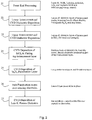
- the manufacturing process 20 is now described in more detail referring to Figs. 2 , 3(a) , 3(b) and 3(c) , and the steps are 21 to 27 inclusive.
- a substrate 41 of silicon is processed with CMOS wells, isolation oxidation, poly-silicon, and implants to form MOS components, as is well known in CMOS processing. Also, in the substrate a temperature-sensitive PNP transistor is formed to provide the sensor 13.
- First, second, and third interconnect levels 42 are formed. This involves three cycles of chemical vapour deposition (CVD) deposition of a porous low-K silicon dioxide dielectric 42(a), and etching and copper plating operations to provide interconnect tracks 42(b). Each cycle finishes in deposition of an etch stop layer 42(c) for limiting the extent of etching in the next cycle.
- the etch stop material is silicon nitride Si 3 N 4 .
- the silicon dioxide, the interconnect metal, and the etch stop of each cycle forms a first interconnect three-level stack 42.
- the use of a low-K dielectric allows low capacitance for faster signal transfer between components.
- Fourth and fifth interconnect levels 43 are formed. There are a further two cycles of dielectric deposition and metal interconnect plating. However, in these two cycles the dielectric is "regular" SiO 2 (non-porous) 43(a) for better structural strength, to counteract the weaker mechanical strength of the porous dielectric in the lower levels 42. Again, these cycles involve standard CMOS techniques.
- the fifth level includes a heating element 43(b) with an internal temperature monitor for instantaneous heating and purging of the humidity sensor 11 with immediate temperature monitoring. Also, as part of developing the fourth and fifth levels, the process adds a thin metal plate for a capacitor top metal (CTM) with a thin layer (0.04 ⁇ m) SiO 2 dielectric between them to form mixed signal metal-insulator-metal (MIM) capacitors for both of the A-to-D converters.
- CTM capacitor top metal
- MIM mixed signal metal-insulator-metal
- An interconnect/sensing layer 44 is formed. This is simply a next iteration or cycle following from the previous interconnect and plating cycles and indeed the dielectric is the same as for the immediately preceding cycles, "regular" SiO 2 .
- humidity-sensing capacitive interdigitated fingers (electrodes) 45 and reference capactive interdigitated fingers (electrodes) 46 are formed. The size and spacing of the fingers is chosen to suit the application. In this embodiment the fingers 45 and 46 have a spacing of 0.5 ⁇ m. The arrangement is shown more clearly in Fig. 3(b) .
- Each actual capacitive structure is about the size of a bond pad, allowing each finger to have a total length of 4000 ⁇ m. For a metal thickness of 1 ⁇ m this gives a sensor capacitance of 0.276 pF. However, the capacitance between two closely-spaced narrow conductors can be about 10% to 30% greater than the simple parallel plate calculated value, due to fringing components.
- a passivation layer 48 is deposited by CVD in a manner similar to that of the conventional etch stop layers as it is also of Si 3 N 4 .
- the passivation layer 48 is, however, approximately 3-5 ⁇ m thick to offer physical protection and a moisture barrier for the device 1.
- That part of the passivation layer 48 over the sensing electrodes 45 is etched to a depth of 90% to leave a thin Si 3 N 4 layer 48(a) of approximately 0.1 ⁇ m depth over the sensing electrodes.
- the same material as is used as a dielectric in the first three levels is now deposited by CVD in the recess formed in step 26.
- the Si 3 N 4 layer is over the sensing component and it acts as a barrier to ingress of the moisture being sensed as such penetration may corrode the electrodes in high humidity environments.
- the sensing is therefore based on use of the spring effect, as set out below.
- the sensor 1 relies on this fringe component 55 of the field between the electrodes.
- the fringe component is about 25 to 50fF.
- This converter is shown in Fig. 4 in which the sensing fingers 45 are Cs and the reference fingers 46 are Cr.
- These capacitances form the differential front-end of a second-order over-sampled sigma-delta modulator, illustrating the level of integration between the sensor and converter components.
- Vr and Vs provide scale and offset compensation. Very high resolution is achieved by trading off the number of samples per second and over-sampling ratio using the decimation filters.
- porous material 50 is deposited (or printed) on top of passivation 51, eliminating extra etching steps.
- the passivation thickness is about 3 ⁇ m for example, then the spacing of the sensor capacitor fingers 45 must be increased to about 5 ⁇ m or more in order that the fringe capacitance component still represents a measurable ratio of the total capacitance.
- total capacitance is now reduced to about 27fF, with the variable fringing component now being in the region of 3 to 5 fF.
- Humidity variations of 1% or 2% now produce capacitance variations of less than a femtoFarad - still detectable by the highly over-sampled differential sigma-delta high-resolution converter. 18 bits of resolution also provides a very large dynamic range, enabling the converter to easily cope with the highly variable and non-linear capacitance-versus-humidity characteristics of different oxides and different pore sizes from wafer to wafer and lot to lot.
- CMOS processing is used, with no extra processing steps required.
- Polyimide is often used as a 'stress relief coating layer on silicon chips.
- the polyimide placement is usually determined by a slightly oversized version of the bond-pad mask.
- the polyimide mask includes an extra opening to eliminate polyamide 60 from over the reference capacitor. Since polyimide is porous, the portion over the sensing capacitor now experiences a minute change in capacitance versus humidity.
- porous low-K oxide dielectric is used in all interconnect levels of the device, so the sensor device has a porous low-K dielectric 70 between capacitive interdigitated fingers 71.
- the surface 72 above the sensing fingers 71 is exposed for ingress of moisture into the dielectric between the fingers during the bond-pad etch.
- This embodiment has the advantage of using the standard CMOS process with no extra masks required. However, it allows access by the moisture to the capacitive fingers 71. However, for many applications this is not a problem, for example a low-humidity office environment where the sensor only experiences a few millivolts applied for a few milliseconds once every few minutes.
- Fig. 8 shows a simple potting arrangement for enclosing the single-chip wireless sensor.
- the sensor 1 is bonded to a battery 80 by conductive adhesive 81 and there is encapsulation 82.
- a former is used to keep the area over the sensing component clear. All other areas are enclosed by the encapsulant 82, which affords physical protection, as well as protection of the chip and battery terminals from corrosion or electrolytic degradation if exposed continuously to high moisture environments. No metal is exposed anywhere, except for an RF antenna wire 83.
- a substrate PNP temperature sensor 13 is also developed as an integral part of the substrate 41, as shown in Fig. 3(a) .
- the 12-bit SAR converter 14 is shown. This measures the Vbe voltage of the PNP, or the temperature-dependent resistance of the metal heater monitor in a bridge configuration as shown.
- the converter achieves 12 bit resolution without any calibration circuits, as follows.
- the capacitor array for the converter 14 is in the center of the level, and it is surrounded by eight similar dummy arrays 90 to ensure constant topography and excellent matching of the key array capacitors in the converter 14.
- the array is segmented into 7 upper bits and a 5-bit sub-DAC via coupling capacitor Cc.
- the time-interval counter and part of the microcontroller's interrupt logic are implemented on thick-oxide 3.3V transistors, as shown in Fig 11 .
- the microcontroller On wakeup from power-down, the microcontroller also achieves reduction of noise and substrate crosstalk by operating the sensors, converters, and radio transceiver sequentially.
- the LNA is designed to have extra low power and low noise operation.
- This is enabled by copper inductors on the fifth or sixth levels, and the use of strained silicon MOS devices for the front-end LNA, see Fig. 12 .
- This diagram shows a thin layer of Silicon-Germanium 100, over which there is a thin strained silicon layer 101, with higher carrier mobility than regular silicon.
- the polysilicon gate 102 creates a channel in the strained silicon region.
- the LNA can therefore be biased at lower currents for the same gain, saving battery power.
- Copper has lower resistance than aluminium, giving a higher Q-factor (resulting in higher receiver gain).
- the fifth or sixth level of copper is also thicker (lower resistance), and further away from the substrate (less parasitic capacitances).
- the device 1 forms a node in a wireless network of nodes. This could be a simple point-to-point link or a star or mesh network.
- a fixed frequency is used by all nodes and the wireless interface 3 provides a slow frequency hopping scheme to circumvent interferers. It operates by all nodes using the same frequency initially.
- the nodes move to a different frequency according to an algorithm illustrated in Fig. 13 . There follows synchronisation of all nodes.
- nodes are pre-programmed with the hop sequence for the frequency-hopping scheme to work. Further, they must all be initialised to the same channel so that they can "hop together", typically after installation or battery replacement.
- the installer upon installation (or battery replacement), the installer manually puts the node into "initialise” mode, by, for example, pressing a button.
- the node then switches on its receiver and "listens” for a nearby node transmission (or master beacon), on channel 0 for example. If it receives nothing after an appropriate time, for example a few seconds or minutes (because the current channel might be blocked), it steps to the next channel in the sequence, and again waits and listens.
- it should receive a beacon or data packet from a neighbouring node; it can then re-synchronise its timer, request the hop interval timing, join the sequence, and go to sleep until the next hop and transmit period.
- This initialisation method means the node has to stay "on” in full-power receive mode just once at installation; it can then revert to sleep mode for 99.9% of the time (as defined in the 802.15.4 standard) for the 1 to 3 year lifetime of the battery. Since the 802.15.4 standard allows for sleep periods of up to about 4 minutes, the node could be in full-power receive mode for this duration. In practice this is unlikely, however, since the installer will know about this period. Using a spectrum analyser (or handheld wireless 'sniffer'), he can roughly predict when the next beacon transmission is due, and press the 'initialise' button just before this.
- this diagram shows an example of use of the slow hopping scheme. It is used on a long-distance (200m) link 115 between two buildings 120 and 125 (using a directional 14dBi antenna on a gateway node 126 linked with a computer 127).
- a standard 802.15.4 Zigbee fixed-channel star network of nodes 121 is implemented within the first building 120. This enables multi-vendor interoperable nodes to be installed in a star-network plant monitoring application, whereas the slow-hopping algorithm is employed on the long-distance critical link, which is more at risk of interference.
- the entire humidity sensor since the entire humidity sensor is fabricated in a standard CMOS process, it can be tested - and calibrated - at the normal wafer-level test before wafers are shipped. This takes advantage of the fact that wafer probe and factory test areas are generally operated at a precise humidity level, for example 40% relative humidity.
- This known value can be stored in on-chip Flash EEPROM memory for later use by the microcontroller in correctly calibrating the output value under software control, or it can be used in a non-Flash-EEPROM version of the chip to blow poly fuses to calibrate the sensor at 40% RH.
- This 1-point calibration may be sufficient for many applications, e.g. office air-conditioning control around a setpoint, typically 40%.
- a second calibration point may be required. This is achieved by doing a "second-pass" wafer probe, in an enclosed chamber at 85% RH for example, or a dry-nitrogen dessicant chamber (0.001% RH). Although the second pass wafer test adds some additional cost, it is significantly less than package based testing.
- a thin film 130 of zinc oxide and ferric oxide is deposited over passivation 131 at the location of one of the differential capacitors 132 of the 18-bit Sigma-Delta A-to-D converter 12.
- These oxides are synthesized by a sol-gel process, heated to about 120°C to 200°C then deposited by hybrid-ink-jet deposition.
- the thin-film means that small finger spacings can be used in the sensor structure, and the high-resolution A-to-D converter means that small sensor structures can be used and still result in detectable minute changes of capacitance, even at room temperature operation.
- Fig. 16 shows an alternative embodiment, in which ferric-oxide/zinc-oxide 140 is deposited on top oxide or passivation 141, but is connected directly to electrodes 142 in the top metal layers, forming a resistor whose value can be determined as part of a bridge circuit by the 18-bit converter.
- the device architecture and production process may be adapted for sensing different gases, such as using palladium for hydrogen sensing, Zirconia for SO 2 , H 2 S, or Plasticised Polyvinyl chloride for NO 2 , and WO 3 for iso-butane.
- gases such as using palladium for hydrogen sensing, Zirconia for SO 2 , H 2 S, or Plasticised Polyvinyl chloride for NO 2 , and WO 3 for iso-butane.
- both the conductivity and dielectric constant of the sensing material is changed by the ingressing gas, by adsorbtion, or physisorbtion, or chemisorbtion. Therefore the embodiments of 15 - capacitive - and 16 - resistive - are used alternately or together in conjunction with the on-chip tightly integrated high resolution converter to achieve very low ppm gas concentration measurements.
- a piezo-electric polymer may be applied in the configuration shown in Fig. 16 for sound sensitivity. Transduction is predominantly based on conductivity change.
- a bridge circuit with buffer driving the 18-bit A-to-D converter is employed to capture the audio signal.
- An audio sensor is a useful feature on a remote wireless node, for example to "listen” if a motor is running, if an alarm bell is ringing. Arrangements are needed for this audio due to the 0.1% duty cycle of IEEE802.15.4; the 250Kb/s max data rate in the 802.15.4 2.4GHz band corresponds to a sustained constant data rate of 250 b/s at 0.1% duty cycle.
- a variable-bit-rate audio compressor block (VBR) is employed to achieve 15:1 or better compression ratio, achieving an effective audio bit-rate of 3.75Kb/s - sufficient for many industrial low-grade audio requirements.
- the device may also include an optical emitter 150 and detector 151.
- Highly-directional deep anisotropic etching is employed at the end of normal processing to fully etch away all six or seven layers of dielectric to expose a photodiode light sensor 151, a large PN junction, 200um x 500um, which collects photons and generates a corresponding electrical current.
- the etch also reveals a porous silicon region 150 in this embodiment, created at the start of the process by electrochemical etching of the substrate in this particular region. Passing current through this makes it function as a light emitting diode (LED) due to the well known luminescence property of porous silicon. Isolation trenches placed around the porous region can minimize any currents leaking to the substrate and improve the light efficiency.
- LED light emitting diode
- Electrochemical etching to form porous silicon is well known to those skilled in the art, and available on some CMOS processes, but is non-standard on most CMOS processes.
- An alternative LED construction is a doped polymer organic light emitting device.
- Hybrid Ink-jet printing is used to directly deposit patterned luminescent doped-polymer films, for example polyvinylcarbazol (PVK) film, onto electrodes in the manner shown in Fig. 16 .
- PVK polyvinylcarbazol
- the invention is not limited to the embodiments described but may be varied in construction and detail within the scope of the claims.
- conductors other than copper may be used for the interconnects, such as aluminium.
- the sensor device may be a "stripped down" version of the sensor, a "humidity-to-digital" sensor chip, having no radio or flash memory.
- calibration of the A-to-D and sensor is achieved by blowing various poly fuses in the voltage reference circuit and capacitor array. It should be noted that testing need not involve testing every code of the A-to-D, thereby simplifying testing significantly, and reducing cost.
- some or more of the following features may be provided individually or in combination in a method and device other than as described in the embodiments above:
Landscapes
- Physics & Mathematics (AREA)
- Chemical & Material Sciences (AREA)
- General Physics & Mathematics (AREA)
- Power Engineering (AREA)
- Engineering & Computer Science (AREA)
- Immunology (AREA)
- Electrochemistry (AREA)
- Biochemistry (AREA)
- General Health & Medical Sciences (AREA)
- Life Sciences & Earth Sciences (AREA)
- Health & Medical Sciences (AREA)
- Pathology (AREA)
- Analytical Chemistry (AREA)
- Chemical Kinetics & Catalysis (AREA)
- Condensed Matter Physics & Semiconductors (AREA)
- Computer Hardware Design (AREA)
- Microelectronics & Electronic Packaging (AREA)
- Geometry (AREA)
- Investigating Or Analyzing Materials By The Use Of Electric Means (AREA)
- Investigating Or Analyzing Materials By The Use Of Fluid Adsorption Or Reactions (AREA)
Claims (34)
- Integrierte kapazitive Sensorvorrichtung (1), umfassend:ein kapazitiver Sensor, der kapazitive Sensorelektroden (45, 46) umfasst;MOS-Schaltungen (3, 5, 6, 9, 10, 12, 14) in einem Halbleitersubstrat (41),Verbindungsebenen (42, 43) jeweils mit Verbindungsleitern (42b, 43b) und isolierenden Dielektrika (42a, 43a), wobei sich die Ebenen über dem Substrat befinden und die MOS-Schaltungen verbinden,wobei eine oberste Verbindungsebene die kapazitiven Sensorelektroden (45, 46), eingebettet in ein isolierendes Dielektrikum, inkorporiert,wobei sich die MOS-Schaltungen in einer vertikalen Dimension direkt unter dem Sensor befinden undwobei die MOS-Schaltungen einen Mikrocontroller (2) zum Verarbeiten von Signalen von den Sensorelektroden beinhalten.
- Integrierte kapazitive Sensorvorrichtung nach Anspruch 1, wobei der Sensor ein poröses Oxid (49) für das Eindringen von Gas oder Feuchtigkeit, das/die erfasst wird, umfasst.
- Integrierte kapazitive Sensorvorrichtung nach Anspruch 2, wobei das poröse Oxid (49) kohlenstoffdotiertes SiO2 ist.
- Integrierte kapazitive Sensorvorrichtung nach einem der vorangehenden Ansprüche, wobei der Sensor eine Passivierungsschicht (48) über den kapazitiven Sensorelektroden umfasst.
- Integrierte kapazitive Sensorvorrichtung nach Anspruch 4, wobei das poröse Oxid (50) auf der Passivierungsschicht (48) abgeschieden ist und die MOS-Schaltungen Änderungen in einem Randfeld zwischen den Elektroden detektieren.
- Integrierte kapazitive Sensorvorrichtung nach Anspruch 4 oder 5, umfassend Ätzstoppschichten (42(c)) zwischen den Verbindungsebenen, und wobei die Passivierungsschicht (48) aus derselben Zusammensetzung wie das Ätzstoppmaterial besteht.
- Integrierte kapazitive Sensorvorrichtung nach Anspruch 6, wobei die Passivierungsschicht (48) aus einer Si3N4-Zusammensetzung besteht.
- Integrierte kapazitive Sensorvorrichtung nach einem der Ansprüche 4 bis 7, wobei die Passivierungsschicht (48) über den Erfassungselektroden ausgespart ist.
- Integrierte kapazitive Sensorvorrichtung nach Anspruch 8, wobei sich in der Aussparung ein poröser Oxidfilm (49) befindet.
- Integrierte kapazitive Sensorvorrichtung nach Anspruch 9, wobei sich das poröse Oxid (70) zwischen den Elektroden (71) befindet und freiliegt.
- Integrierte kapazitive Sensorvorrichtung nach einem der vorangehenden Ansprüche, wobei die MOS-Schaltungen einen Temperatursensor (13) beinhalten.
- Integrierte kapazitive Sensorvorrichtung nach Anspruch 11, wobei der Temperatursensor (13) einen PNP-Transistor umfasst.
- Integrierte kapazitive Sensorvorrichtung nach Anspruch 11 oder 12, wobei der Mikrocontroller (2) zum Verarbeiten von sowohl Gas- oder Feuchtigkeitssignalen von dem Gas- oder Feuchtigkeitssensor als auch Temperatursignalen von dem Temperatursensor, um eine verbesserte Ausgabe bereitzustellen, dient.
- Integrierte kapazitive Sensorvorrichtung nach Anspruch 13, wobei die verbesserte Ausgabe temperaturberichtigte Gas- oder Feuchtigkeitsangaben sind.
- Integrierte kapazitive Sensorvorrichtung nach Anspruch 1, wobei der Sensor Polyimid (60) umfasst, das über den Sensorelektroden abgeschieden ist.
- Integrierte kapazitive Sensorvorrichtung nach einem der vorangehenden Ansprüche, wobei die MOS-Schaltungen einen A/D-Wandler (12, 14) beinhalten, der zwischen die kapazitiven Sensorelektroden und den Prozessor geschaltet ist.
- Integrierte kapazitive Sensorvorrichtung nach Anspruch 16, wobei der A/D-Wandler (14) eine Anordnung (90) von Dummy-Kondensatoren mit einer konstanten Topographie umfasst, die aktive A/D-Wandler-Kondensatoren umgibt.
- Integrierte kapazitive Sensorvorrichtung nach einem der vorangehenden Ansprüche, ferner umfassend eine Leuchtdiode (150).
- Integrierte kapazitive Sensorvorrichtung nach Anspruch 18, wobei die Diode in einem tiefen Graben zu einer tieferliegenden Verbindungsebene lateral von den Sensorelektroden gebildet ist.
- Integrierte kapazitive Sensorvorrichtung nach einem der vorangehenden Ansprüche, wobei die Vorrichtung eine Fotodetektordiode (151) umfasst.
- Integrierte kapazitive Sensorvorrichtung nach Anspruch 20, wobei sich die Diode in einem tiefen Graben in einer tieferliegenden Verbindungsebene lateral von den kapazitiven Sensorelektroden befindet.
- Integrierte kapazitive Sensorvorrichtung nach einem der vorangehenden Ansprüche, wobei die MOS-Schaltungen einen drahtlosen Transceiver (3, 4) und einen rauscharmen Verstärker (100-102) beinhalten.
- Integrierte kapazitive Sensorvorrichtung nach Anspruch 22, wobei der drahtlose Transceiver zur Kommunikation mit anderen Knoten in einem Netzwerk dient und er ein Mittel zum Schalten der Kanalfrequenz gemäß einem Niederfrequenzkanal-Schaltschema bei Detektion von Interferenz umfasst.
- Integrierte kapazitive Sensorvorrichtung nach Anspruch 22 oder 23, wobei eine Verbindungsebene Kupferspulen für den rauscharmen Verstärker beinhaltet.
- Integrierte kapazitive Sensorvorrichtung nach Anspruch 24, wobei der rauscharme Verstärker eine Region (101) mit gestrecktem Silicium unter einem Leiter umfasst.
- Integrierte kapazitive Sensorvorrichtung nach Anspruch 24 oder 25, wobei sich die Spulen in einer fünften oder sechsten Verbindungsebene über dem Substrat befinden.
- Integrierte kapazitive Sensorvorrichtung nach einem der vorangehenden Ansprüche, wobei der Sensor Kontaktstellen (142) an einer oberen Oberfläche der Vorrichtung und ein Detektionselement (140), das zwischen die Kontaktstellen geschaltet ist, umfasst.
- Integrierte kapazitive Sensorvorrichtung nach Anspruch 27, wobei das Element ein gaserfassender Dünnfilm (140) ist.
- Integrierte kapazitive Sensorvorrichtung nach Anspruch 28, wobei das Element (140) aus einer Zinkoxidzusammensetzung besteht.
- Integrierte kapazitive Sensorvorrichtung nach Anspruch 27, wobei das Element Ton detektiert und die MOS-Schaltungen einen Audioprozessor zum Verarbeiten von Signalen von den Elementen umfassen.
- Verfahren zum Produzieren einer kapazitiven Sensorvorrichtung nach einem der vorangehenden Ansprüche, wobei das Verfahren die folgenden Schritte umfasst:Herstellen (21) der MOS-Schaltungen in dem Substrat,Herstellen (22-23) der Verbindungsebenen in aufeinanderfolgenden Herstellungszyklen gemäß einem Verbindungsdesign zum Verbinden der MOS-Schaltungen undHerstellen (24-27) der Sensorelektroden und des Dielektrikums in einer Endverbindungsebene.
- Verfahren nach Anspruch 31, umfassend den weiteren Schritt des Abscheidens (26) einer Passivierungsschicht über der obersten Verbindungsebene.
- Verfahren nach Anspruch 32, umfassend die Schritte des Abscheidens (25) einer Ätzstoppschicht über jeder Schicht aus Dielektrikum in den Verbindungsebenen und Abscheiden von Ätzstoppmaterial über dem Dielektrikum der obersten Verbindungsebene zum Bereitstellen der Passivierungsschicht.
- Verfahren nach einem der Ansprüche 31 bis 33, wobei poröses Oxid als ein Dielektrikum in tieferliegenden Verbindungsebenen bereitgestellt ist und nicht poröses Oxid als ein Dielektrikum in oberen Verbindungsebenen verwendet wird.
Applications Claiming Priority (2)
| Application Number | Priority Date | Filing Date | Title |
|---|---|---|---|
| US55856504P | 2004-04-02 | 2004-04-02 | |
| PCT/IE2005/000033 WO2005095936A1 (en) | 2004-04-02 | 2005-03-30 | An integrated electronic sensor |
Publications (2)
| Publication Number | Publication Date |
|---|---|
| EP1730506A1 EP1730506A1 (de) | 2006-12-13 |
| EP1730506B1 true EP1730506B1 (de) | 2018-09-26 |
Family
ID=34962453
Family Applications (1)
| Application Number | Title | Priority Date | Filing Date |
|---|---|---|---|
| EP05718823.7A Not-in-force EP1730506B1 (de) | 2004-04-02 | 2005-03-30 | Integrierter elektronischer sensor |
Country Status (5)
| Country | Link |
|---|---|
| US (7) | US7554134B2 (de) |
| EP (1) | EP1730506B1 (de) |
| JP (1) | JP2007535662A (de) |
| CN (2) | CN1961209A (de) |
| WO (1) | WO2005095936A1 (de) |
Families Citing this family (89)
| Publication number | Priority date | Publication date | Assignee | Title |
|---|---|---|---|---|
| WO2005095936A1 (en) * | 2004-04-02 | 2005-10-13 | Timothy Cummins | An integrated electronic sensor |
| US8357958B2 (en) * | 2004-04-02 | 2013-01-22 | Silicon Laboratories Inc. | Integrated CMOS porous sensor |
| WO2007036922A1 (en) * | 2005-09-30 | 2007-04-05 | Timothy Cummins | An integrated electronic sensor |
| EP1889293B1 (de) * | 2005-05-26 | 2013-03-06 | Nxp B.V. | Elektronische einrichtung |
| US8079248B2 (en) * | 2005-11-17 | 2011-12-20 | Nxp B.V. | Moisture sensor |
| US7420365B2 (en) * | 2006-03-15 | 2008-09-02 | Honeywell International Inc. | Single chip MR sensor integrated with an RF transceiver |
| US20070235877A1 (en) * | 2006-03-31 | 2007-10-11 | Miriam Reshotko | Integration scheme for semiconductor photodetectors on an integrated circuit chip |
| US7700975B2 (en) * | 2006-03-31 | 2010-04-20 | Intel Corporation | Schottky barrier metal-germanium contact in metal-germanium-metal photodetectors |
| DE102006019534A1 (de) * | 2006-04-27 | 2007-11-08 | CiS Institut für Mikrosensorik gGmbH | Mikrosensor |
| DE102006036646A1 (de) * | 2006-08-03 | 2008-02-07 | Innovative Sensor Technology Ist Ag | Verfahren zur Bestimmung der relativen Feuchte eines Mediums und entsprechende Vorrichtung |
| DE102006037243B4 (de) * | 2006-08-09 | 2010-06-02 | Siemens Ag | Netzwerk zur drahtlosen Übertragung von Daten |
| KR20080041912A (ko) * | 2006-11-08 | 2008-05-14 | 삼성전자주식회사 | 감도 제어가 가능한 씨모스 이미지 센서의 픽셀 회로 |
| US8178953B2 (en) | 2008-09-30 | 2012-05-15 | Infineon Technologies Ag | On-chip RF shields with front side redistribution lines |
| US7948064B2 (en) * | 2008-09-30 | 2011-05-24 | Infineon Technologies Ag | System on a chip with on-chip RF shield |
| US8063469B2 (en) * | 2008-09-30 | 2011-11-22 | Infineon Technologies Ag | On-chip radio frequency shield with interconnect metallization |
| US8169059B2 (en) * | 2008-09-30 | 2012-05-01 | Infineon Technologies Ag | On-chip RF shields with through substrate conductors |
| US8889548B2 (en) | 2008-09-30 | 2014-11-18 | Infineon Technologies Ag | On-chip RF shields with backside redistribution lines |
| US8124953B2 (en) | 2009-03-12 | 2012-02-28 | Infineon Technologies Ag | Sensor device having a porous structure element |
| EP2282333B1 (de) | 2009-07-27 | 2013-03-20 | Nxp B.V. | Integrierte Schaltung mit Feuchtesensor |
| CN101738422B (zh) | 2009-12-23 | 2012-09-05 | 北京宝力马传感技术有限公司 | 一种湿度测量装置及方法 |
| KR101665669B1 (ko) * | 2010-03-04 | 2016-10-13 | 삼성전자주식회사 | 반도체 소자 및 그 형성 방법 |
| US8927909B2 (en) * | 2010-10-11 | 2015-01-06 | Stmicroelectronics, Inc. | Closed loop temperature controlled circuit to improve device stability |
| EP2508881B1 (de) * | 2011-04-04 | 2019-01-23 | Sensirion AG | Prüfen eines Feuchtigkeitssensors |
| EP2508874B1 (de) * | 2011-04-08 | 2019-06-05 | ams international AG | Kapazitiver Sensor, integrierte Schaltung, elektronische Vorrichtung und Verfahren |
| EP2554980B1 (de) * | 2011-08-03 | 2014-06-25 | Nxp B.V. | Integrierte Schaltung mit Sensor und Verfahren zur Herstellung solch einer integrierten Schaltung |
| US8852513B1 (en) | 2011-09-30 | 2014-10-07 | Silicon Laboratories Inc. | Systems and methods for packaging integrated circuit gas sensor systems |
| US8691609B1 (en) | 2011-09-30 | 2014-04-08 | Silicon Laboratories Inc. | Gas sensor materials and methods for preparation thereof |
| US8669131B1 (en) | 2011-09-30 | 2014-03-11 | Silicon Laboratories Inc. | Methods and materials for forming gas sensor structures |
| US9164052B1 (en) | 2011-09-30 | 2015-10-20 | Silicon Laboratories Inc. | Integrated gas sensor |
| EP2623969B1 (de) * | 2012-01-31 | 2014-05-14 | Nxp B.V. | Integrierte Schaltung und Herstellungsverfahren |
| EP2645091B1 (de) | 2012-03-30 | 2018-10-17 | ams international AG | Integrierte Schaltung mit Gassensor |
| EP2657691B1 (de) * | 2012-04-25 | 2018-08-29 | E+E Elektronik Ges.m.b.H. | Feuchtesensor-Anordnung |
| EP2677307B1 (de) | 2012-06-21 | 2016-05-11 | Nxp B.V. | Integrierte Schaltung mit Sensoren und Herstellungsverfahren |
| CN102721429B (zh) * | 2012-06-21 | 2015-06-24 | 昆山诺科传感器集成有限公司 | 频率输出温湿度变送器 |
| US9287219B2 (en) | 2012-07-25 | 2016-03-15 | Silicon Laboratories Inc. | Radiation-blocking structures |
| EP2720034B1 (de) * | 2012-10-12 | 2016-04-27 | ams International AG | Integrierte Schaltung mit relativem Feuchtigkeitssensor und Wärmeleitfähigkeits Gassensor |
| CN103115569B (zh) * | 2012-10-22 | 2016-05-04 | 深圳市嘉瀚科技有限公司 | 具有无线传输功能的整体集成式光电传感器 |
| EP2762865A1 (de) * | 2013-01-31 | 2014-08-06 | Sensirion Holding AG | Chemische Sensor und Verfahren zur Herstellung solch eines chemischen Sensors |
| US10175188B2 (en) | 2013-03-15 | 2019-01-08 | Robert Bosch Gmbh | Trench based capacitive humidity sensor |
| JP6286845B2 (ja) * | 2013-03-22 | 2018-03-07 | 富士通株式会社 | 熱電素子搭載モジュール及びその製造方法 |
| US9234859B2 (en) * | 2013-03-28 | 2016-01-12 | Stmicroelectronics S.R.L. | Integrated device of a capacitive type for detecting humidity, in particular manufactured using a CMOS technology |
| US10323980B2 (en) * | 2013-03-29 | 2019-06-18 | Rensselaer Polytechnic Institute | Tunable photocapacitive optical radiation sensor enabled radio transmitter and applications thereof |
| EP2793018A1 (de) * | 2013-04-19 | 2014-10-22 | Nxp B.V. | Auf Wärmeleitfähigkeit basierender Gassensor |
| CN103209002B (zh) * | 2013-04-23 | 2015-12-23 | 中国科学院深圳先进技术研究院 | 用于微型无线传感器节点的数据传输装置 |
| SG11201509385TA (en) * | 2013-05-17 | 2015-12-30 | fybr | Distributed remote sensing system component interface |
| EP2996901A4 (de) | 2013-05-17 | 2017-01-25 | Fybr | Gateway für verteiltes fernmesssystem |
| CN104981688B (zh) * | 2013-05-29 | 2018-07-13 | 罗斯蒙特分析公司 | 具有湿度和温度补偿的硫化氢气体探测器 |
| US10177781B2 (en) | 2013-06-24 | 2019-01-08 | Silicon Laboratories Inc. | Circuit including a switched capacitor bridge and method |
| WO2015086654A1 (en) * | 2013-12-12 | 2015-06-18 | Altra Tech Limited | A capacitive sensor and method of use |
| CN105980558B (zh) | 2013-12-12 | 2021-08-24 | 阿尔查技术有限公司 | 样品制备方法和设备 |
| TWI523808B (zh) * | 2014-01-29 | 2016-03-01 | 先技股份有限公司 | 微機電氣體感測裝置 |
| KR20150116209A (ko) * | 2014-04-07 | 2015-10-15 | 주식회사 이노칩테크놀로지 | 센서 소자 |
| KR102238937B1 (ko) | 2014-07-22 | 2021-04-09 | 주식회사 키 파운드리 | 배선 사이의 중공에 형성된 습도 센서 및 그 제조 방법 |
| EP3037810B1 (de) * | 2014-12-23 | 2017-10-25 | EM Microelectronic-Marin SA | Verbesserter feuchtigkeitssensor |
| CN104614294A (zh) * | 2014-12-31 | 2015-05-13 | 北京工业大学 | 一种基于Zigbee无线通信技术的分层异构空气质量实时监测模型 |
| CN104627947B (zh) * | 2015-02-09 | 2016-02-10 | 江西师范大学 | Cmos湿度传感器及其形成方法 |
| EP3062097A1 (de) * | 2015-02-27 | 2016-08-31 | EM Microelectronic-Marin SA | Feuchtigkeitssensor mit wärmemodul |
| US10055781B2 (en) | 2015-06-05 | 2018-08-21 | Boveda Inc. | Systems, methods and devices for controlling humidity in a closed environment with automatic and predictive identification, purchase and replacement of optimal humidity controller |
| US10909607B2 (en) | 2015-06-05 | 2021-02-02 | Boveda Inc. | Systems, methods and devices for controlling humidity in a closed environment with automatic and predictive identification, purchase and replacement of optimal humidity controller |
| US9891183B2 (en) * | 2015-07-07 | 2018-02-13 | Nxp B.V. | Breach sensor |
| US10670554B2 (en) | 2015-07-13 | 2020-06-02 | International Business Machines Corporation | Reconfigurable gas sensor architecture with a high sensitivity at low temperatures |
| EP3163295B1 (de) * | 2015-11-02 | 2020-09-30 | Alpha M.O.S. | System und verfahren zur charakterisierung einer gasprobe |
| CN105675051B (zh) * | 2016-01-12 | 2018-06-05 | 上海申矽凌微电子科技有限公司 | 制造传感器集成电路的方法及使用该方法制造的集成电路 |
| EP3408402A4 (de) | 2016-01-27 | 2019-07-10 | The General Hospital Corporation | Magnetische elektrochemische erfassung |
| US10336606B2 (en) * | 2016-02-25 | 2019-07-02 | Nxp Usa, Inc. | Integrated capacitive humidity sensor |
| US20170287757A1 (en) * | 2016-03-30 | 2017-10-05 | Robert F. Kwasnick | Damage monitor |
| CN105742247B (zh) * | 2016-04-07 | 2019-07-26 | 上海申矽凌微电子科技有限公司 | 传感器集成电路的制造方法及使用该方法制造的集成电路 |
| US10083883B2 (en) * | 2016-06-20 | 2018-09-25 | Applied Materials, Inc. | Wafer processing equipment having capacitive micro sensors |
| CN106124576B (zh) * | 2016-06-28 | 2018-12-18 | 上海申矽凌微电子科技有限公司 | 集成的湿度传感器和多单元气体传感器及其制造方法 |
| CN106082102B (zh) * | 2016-07-12 | 2017-12-15 | 上海申矽凌微电子科技有限公司 | 集成温度湿度气体传感的传感器电路制造方法及传感器 |
| US10254261B2 (en) | 2016-07-18 | 2019-04-09 | Stmicroelectronics Pte Ltd | Integrated air quality sensor that detects multiple gas species |
| US10429330B2 (en) | 2016-07-18 | 2019-10-01 | Stmicroelectronics Pte Ltd | Gas analyzer that detects gases, humidity, and temperature |
| CN106249093A (zh) * | 2016-07-22 | 2016-12-21 | 上海新时达电气股份有限公司 | 自动分辨并检测电气设备中的预埋传感器的装置及其方法 |
| US10557812B2 (en) | 2016-12-01 | 2020-02-11 | Stmicroelectronics Pte Ltd | Gas sensors |
| US10480495B2 (en) * | 2017-05-08 | 2019-11-19 | Emerson Climate Technologies, Inc. | Compressor with flooded start control |
| US11459601B2 (en) | 2017-09-20 | 2022-10-04 | Altratech Limited | Diagnostic device and system |
| US10453791B2 (en) * | 2018-02-06 | 2019-10-22 | Apple Inc. | Metal-on-metal capacitors |
| CN108562697A (zh) * | 2018-03-30 | 2018-09-21 | 歌尔股份有限公司 | 一种室内有害气体监测装置 |
| US10804195B2 (en) * | 2018-08-08 | 2020-10-13 | Qualcomm Incorporated | High density embedded interconnects in substrate |
| JP7167396B2 (ja) * | 2018-11-16 | 2022-11-09 | ミネベアミツミ株式会社 | 湿度検出装置及び故障判定方法 |
| CN209326840U (zh) | 2018-12-27 | 2019-08-30 | 热敏碟公司 | 压力传感器及压力变送器 |
| CN111696952A (zh) * | 2019-03-13 | 2020-09-22 | 住友电工光电子器件创新株式会社 | 微波集成电路 |
| US11397047B2 (en) * | 2019-04-10 | 2022-07-26 | Minebea Mitsumi Inc. | Moisture detector, moisture detection method, electronic device, and log output system |
| EP3795986B1 (de) | 2019-09-19 | 2023-06-07 | Université catholique de Louvain | Herstellungsverfahren für mehrpixel-gasmikrosensoren mit mehrfacherfassungsfähigkeiten |
| KR20220023074A (ko) * | 2020-08-20 | 2022-03-02 | 삼성전자주식회사 | 반도체 패키지 테스트 장치 및 방법 |
| US11855019B2 (en) | 2021-02-11 | 2023-12-26 | Globalfoundries Singapore Pte. Ltd. | Method of forming a sensor device |
| CN113252734B (zh) * | 2021-06-22 | 2021-09-24 | 电子科技大学 | 一种电阻型气体传感器柔性电路及气体浓度计算方法 |
| US20240319127A1 (en) * | 2023-03-24 | 2024-09-26 | Qualcomm Incorporated | Moisture sensor having integrated heating element |
| CN118500576B (zh) * | 2024-07-18 | 2024-09-13 | 国鲸科技(广东横琴粤澳深度合作区)有限公司 | 一种基于网状传感器的温度实时监测系统 |
Citations (1)
| Publication number | Priority date | Publication date | Assignee | Title |
|---|---|---|---|---|
| US4144636A (en) * | 1976-07-02 | 1979-03-20 | International Business Machines Corporation | Method for manufacture of a moisture sensor |
Family Cites Families (54)
| Publication number | Priority date | Publication date | Assignee | Title |
|---|---|---|---|---|
| GB1586117A (en) * | 1977-06-22 | 1981-03-18 | Rosemount Eng Co Ltd | Solid state sensor element |
| US4165642A (en) | 1978-03-22 | 1979-08-28 | Lipp Robert J | Monolithic CMOS digital temperature measurement circuit |
| US4419021A (en) * | 1980-02-04 | 1983-12-06 | Matsushita Electric Industrial Co., Ltd. | Multi-functional sensing or measuring system |
| JPS58111747A (ja) | 1981-12-25 | 1983-07-02 | Yamatake Honeywell Co Ltd | ガスセンサおよびその製造方法 |
| CA1216330A (en) | 1983-02-07 | 1987-01-06 | Junji Manaka | Low power gas detector |
| US4656463A (en) | 1983-04-21 | 1987-04-07 | Intelli-Tech Corporation | LIMIS systems, devices and methods |
| US4542640A (en) | 1983-09-15 | 1985-09-24 | Clifford Paul K | Selective gas detection and measurement system |
| JPS6066145A (ja) | 1983-09-20 | 1985-04-16 | Omron Tateisi Electronics Co | 外部雰囲気検知装置 |
| JPS60242354A (ja) | 1984-05-16 | 1985-12-02 | Sharp Corp | Fet型センサ |
| JPS6157847A (ja) | 1984-08-29 | 1986-03-24 | Sharp Corp | 電界効果型湿度センサ |
| US4931381A (en) * | 1985-08-12 | 1990-06-05 | Hoechst Celanese Corporation | Image reversal negative working O-quinone diazide and cross-linking compound containing photoresist process with thermal curing treatment |
| GB8606045D0 (en) | 1986-03-12 | 1986-04-16 | Emi Plc Thorn | Gas sensitive device |
| JPH06105232B2 (ja) * | 1986-07-17 | 1994-12-21 | 株式会社東芝 | 絶縁ゲ−ト電界効果型感湿素子 |
| JPS63103957A (ja) | 1986-10-20 | 1988-05-09 | Seiko Epson Corp | 湿度検出器 |
| US4793181A (en) | 1987-06-02 | 1988-12-27 | Djorup Robert Sonny | Constant temperature sorption hygrometer |
| US4831381A (en) * | 1987-08-11 | 1989-05-16 | Texas Instruments Incorporated | Charge redistribution A/D converter with reduced small signal error |
| JPH01196558A (ja) * | 1988-02-01 | 1989-08-08 | Takara Kogyo Kk | 湿度センサ |
| US4876890A (en) | 1988-06-29 | 1989-10-31 | Uop | Moisture sensing apparatus and method |
| JPH02232901A (ja) * | 1989-03-07 | 1990-09-14 | Seiko Epson Corp | 湿度センサ |
| US5120421A (en) * | 1990-08-31 | 1992-06-09 | The United States Of America As Represented By The United States Department Of Energy | Electrochemical sensor/detector system and method |
| JP3041491B2 (ja) | 1991-06-06 | 2000-05-15 | 株式会社トーキン | 湿度センサ |
| CA2066929C (en) * | 1991-08-09 | 1996-10-01 | Katsuji Kimura | Temperature sensor circuit and constant-current circuit |
| US5481129A (en) * | 1991-10-30 | 1996-01-02 | Harris Corporation | Analog-to-digital converter |
| DE19623517C1 (de) | 1996-06-12 | 1997-08-21 | Siemens Ag | MOS-Transistor für biotechnische Anwendungen |
| US6399970B2 (en) | 1996-09-17 | 2002-06-04 | Matsushita Electric Industrial Co., Ltd. | FET having a Si/SiGeC heterojunction channel |
| DE19641777C2 (de) * | 1996-10-10 | 2001-09-27 | Micronas Gmbh | Verfahren zum Herstellen eines Sensors mit einer Metallelektrode in einer MOS-Anordnung |
| GB2321336B (en) * | 1997-01-15 | 2001-07-25 | Univ Warwick | Gas-sensing semiconductor devices |
| US5878332A (en) * | 1997-02-07 | 1999-03-02 | Eic Enterprises Corporation | Multiple frequency RF transceiver |
| EP0882978A1 (de) * | 1997-06-04 | 1998-12-09 | STMicroelectronics S.r.l. | Integrierte Halbleitervorrichtung mit einem auf chemischer Widerstandsfähigkeit beruhenden Microgassensor und Verfahren zu deren Herstellung |
| EP0895090B1 (de) | 1997-07-31 | 2003-12-10 | STMicroelectronics S.r.l. | Verfahren zum Herstellen hochempfindlicher integrierter Beschleunigungs- und Gyroskopsensoren und Sensoren, die derartig hergestellt werden |
| JP3514361B2 (ja) * | 1998-02-27 | 2004-03-31 | Tdk株式会社 | チップ素子及びチップ素子の製造方法 |
| US6288442B1 (en) | 1998-09-10 | 2001-09-11 | Micron Technology, Inc. | Integrated circuit with oxidation-resistant polymeric layer |
| JP2000299438A (ja) * | 1999-04-15 | 2000-10-24 | Hitachi Ltd | 半導体集積回路 |
| DE19924906C2 (de) | 1999-05-31 | 2001-05-31 | Daimler Chrysler Ag | Halbleiter-Gassensor, Gassensorsystem und Verfahren zur Gasanalyse |
| WO2001042776A1 (de) | 1999-12-08 | 2001-06-14 | Sensirion Ag | Kapazitiver sensor |
| US6673644B2 (en) * | 2001-03-29 | 2004-01-06 | Georgia Tech Research Corporation | Porous gas sensors and method of preparation thereof |
| US6580600B2 (en) | 2001-02-20 | 2003-06-17 | Nippon Soken, Inc. | Capacitance type humidity sensor and manufacturing method of the same |
| US6632478B2 (en) * | 2001-02-22 | 2003-10-14 | Applied Materials, Inc. | Process for forming a low dielectric constant carbon-containing film |
| US6484559B2 (en) | 2001-02-26 | 2002-11-26 | Lucent Technologies Inc. | Odor sensing with organic transistors |
| US6348407B1 (en) * | 2001-03-15 | 2002-02-19 | Chartered Semiconductor Manufacturing Inc. | Method to improve adhesion of organic dielectrics in dual damascene interconnects |
| US20030010988A1 (en) * | 2001-07-11 | 2003-01-16 | Motorola, Inc. | Structure and method for fabricating semiconductor structures with integrated optical components and controller |
| JP4501320B2 (ja) * | 2001-07-16 | 2010-07-14 | 株式会社デンソー | 容量式湿度センサ |
| WO2003028106A2 (en) | 2001-09-24 | 2003-04-03 | Amberwave Systems Corporation | Rf circuits including transistors having strained material layers |
| US6673664B2 (en) * | 2001-10-16 | 2004-01-06 | Sharp Laboratories Of America, Inc. | Method of making a self-aligned ferroelectric memory transistor |
| US6724612B2 (en) | 2002-07-09 | 2004-04-20 | Honeywell International Inc. | Relative humidity sensor with integrated signal conditioning |
| JP3869815B2 (ja) | 2003-03-31 | 2007-01-17 | Necエレクトロニクス株式会社 | 半導体集積回路装置 |
| US7053425B2 (en) | 2003-11-12 | 2006-05-30 | General Electric Company | Gas sensor device |
| JP4065855B2 (ja) | 2004-01-21 | 2008-03-26 | 株式会社日立製作所 | 生体および化学試料検査装置 |
| JP3994975B2 (ja) | 2004-02-27 | 2007-10-24 | 株式会社デンソー | 容量式湿度センサ |
| JP4553611B2 (ja) | 2004-03-15 | 2010-09-29 | 三洋電機株式会社 | 回路装置 |
| WO2005095936A1 (en) | 2004-04-02 | 2005-10-13 | Timothy Cummins | An integrated electronic sensor |
| WO2007036922A1 (en) | 2005-09-30 | 2007-04-05 | Timothy Cummins | An integrated electronic sensor |
| US7096716B2 (en) | 2004-11-03 | 2006-08-29 | Avago Technologies Ecbu Ip (Singapore) Pte. Ltd. | Integration of thermal regulation and electronic fluid sensing |
| DE602006000295T2 (de) | 2005-09-21 | 2008-11-06 | Adixen Sensistor Ab | Wasserstoffgassensitiver Halbleitersensor |
-
2005
- 2005-03-30 WO PCT/IE2005/000033 patent/WO2005095936A1/en active Application Filing
- 2005-03-30 JP JP2007505733A patent/JP2007535662A/ja active Pending
- 2005-03-30 US US11/092,725 patent/US7554134B2/en active Active
- 2005-03-30 CN CNA2005800178446A patent/CN1961209A/zh active Pending
- 2005-03-30 EP EP05718823.7A patent/EP1730506B1/de not_active Not-in-force
- 2005-03-30 CN CN2012102889459A patent/CN102854229A/zh active Pending
-
2009
- 2009-05-28 US US12/453,965 patent/US8648395B2/en not_active Expired - Fee Related
-
2010
- 2010-12-22 US US12/975,846 patent/US8507954B2/en not_active Expired - Fee Related
- 2010-12-23 US US12/977,370 patent/US8507955B2/en not_active Expired - Fee Related
- 2010-12-23 US US12/977,358 patent/US8497531B2/en not_active Expired - Fee Related
-
2012
- 2012-06-12 US US13/494,392 patent/US20120256236A1/en not_active Abandoned
-
2015
- 2015-06-24 US US14/748,303 patent/US20150316498A1/en not_active Abandoned
Patent Citations (1)
| Publication number | Priority date | Publication date | Assignee | Title |
|---|---|---|---|---|
| US4144636A (en) * | 1976-07-02 | 1979-03-20 | International Business Machines Corporation | Method for manufacture of a moisture sensor |
Also Published As
| Publication number | Publication date |
|---|---|
| WO2005095936A1 (en) | 2005-10-13 |
| US20150316498A1 (en) | 2015-11-05 |
| US8497531B2 (en) | 2013-07-30 |
| US8507954B2 (en) | 2013-08-13 |
| US20050218465A1 (en) | 2005-10-06 |
| CN102854229A (zh) | 2013-01-02 |
| CN1961209A (zh) | 2007-05-09 |
| US20110089439A1 (en) | 2011-04-21 |
| EP1730506A1 (de) | 2006-12-13 |
| US7554134B2 (en) | 2009-06-30 |
| US20110089472A1 (en) | 2011-04-21 |
| US20120256236A1 (en) | 2012-10-11 |
| US20110098937A1 (en) | 2011-04-28 |
| US8507955B2 (en) | 2013-08-13 |
| US20090273009A1 (en) | 2009-11-05 |
| US8648395B2 (en) | 2014-02-11 |
| JP2007535662A (ja) | 2007-12-06 |
Similar Documents
| Publication | Publication Date | Title |
|---|---|---|
| EP1730506B1 (de) | Integrierter elektronischer sensor | |
| EP1929285B1 (de) | Integrierter elektronischer sensor und verfahren zu seiner herstellung | |
| US8357958B2 (en) | Integrated CMOS porous sensor | |
| US20150338360A1 (en) | Integrated CMOS Porous Sensor | |
| US20030039586A1 (en) | Membrane type gas sensor and method for manufacturing membrane type gas sensor | |
| WO2012152308A1 (en) | Ion sensitive field effect transistor | |
| US7355200B2 (en) | Ion-sensitive field effect transistor and method for producing an ion-sensitive field effect transistor | |
| WO2007122287A1 (en) | Micro hotplate semiconductive gas sensor | |
| US6464940B1 (en) | pH sensor and pH measurement method employing the same | |
| US20030037590A1 (en) | Method of self-testing a semiconductor chemical gas sensor including an embedded temperature sensor | |
| US7390682B2 (en) | Method for testing metal-insulator-metal capacitor structures under high temperature at wafer level | |
| IES20050180A2 (en) | An integrated electronic sensor | |
| IE84228B1 (en) | An integrated electronic sensor | |
| IE20050180U1 (en) | An integrated electronic sensor | |
| IES84059Y1 (en) | An integrated electronic sensor | |
| IE84764B1 (en) | An integrated electronic sensor | |
| Stoev et al. | An integrated gas sensor on silicon substrate with sensitive SnOx layer | |
| KR100504177B1 (ko) | 반도체 가스 센서 및 그 제조 방법 | |
| US20200333284A1 (en) | High surface area electrode for electrochemical sensor | |
| JPS6258456B2 (de) |
Legal Events
| Date | Code | Title | Description |
|---|---|---|---|
| PUAI | Public reference made under article 153(3) epc to a published international application that has entered the european phase |
Free format text: ORIGINAL CODE: 0009012 |
|
| 17P | Request for examination filed |
Effective date: 20061004 |
|
| AK | Designated contracting states |
Kind code of ref document: A1 Designated state(s): AT BE BG CH CY CZ DE DK EE ES FI FR GB GR HU IE IS IT LI LT LU MC NL PL PT RO SE SI SK TR |
|
| DAX | Request for extension of the european patent (deleted) | ||
| 17Q | First examination report despatched |
Effective date: 20090213 |
|
| RAP1 | Party data changed (applicant data changed or rights of an application transferred) |
Owner name: CHIPSENSORS LIMITED |
|
| RIN1 | Information on inventor provided before grant (corrected) |
Inventor name: CUMMINS, TIMOTHY |
|
| RAP1 | Party data changed (applicant data changed or rights of an application transferred) |
Owner name: SILICON LABORATORIES INC. |
|
| STAA | Information on the status of an ep patent application or granted ep patent |
Free format text: STATUS: EXAMINATION IS IN PROGRESS |
|
| GRAP | Despatch of communication of intention to grant a patent |
Free format text: ORIGINAL CODE: EPIDOSNIGR1 |
|
| RIC1 | Information provided on ipc code assigned before grant |
Ipc: H01L 27/15 20060101ALN20180606BHEP Ipc: G01N 27/22 20060101AFI20180606BHEP Ipc: H01L 27/105 20060101ALN20180606BHEP Ipc: G01N 27/12 20060101ALN20180606BHEP |
|
| STAA | Information on the status of an ep patent application or granted ep patent |
Free format text: STATUS: GRANT OF PATENT IS INTENDED |
|
| RIC1 | Information provided on ipc code assigned before grant |
Ipc: H01L 27/15 20060101ALN20180626BHEP Ipc: G01N 27/22 20060101AFI20180626BHEP Ipc: H01L 27/105 20060101ALN20180626BHEP Ipc: G01N 27/12 20060101ALN20180626BHEP |
|
| INTG | Intention to grant announced |
Effective date: 20180712 |
|
| RIN1 | Information on inventor provided before grant (corrected) |
Inventor name: CUMMINS, TIMOTHY |
|
| GRAS | Grant fee paid |
Free format text: ORIGINAL CODE: EPIDOSNIGR3 |
|
| GRAA | (expected) grant |
Free format text: ORIGINAL CODE: 0009210 |
|
| STAA | Information on the status of an ep patent application or granted ep patent |
Free format text: STATUS: THE PATENT HAS BEEN GRANTED |
|
| AK | Designated contracting states |
Kind code of ref document: B1 Designated state(s): AT BE BG CH CY CZ DE DK EE ES FI FR GB GR HU IE IS IT LI LT LU MC NL PL PT RO SE SI SK TR |
|
| REG | Reference to a national code |
Ref country code: GB Ref legal event code: FG4D |
|
| REG | Reference to a national code |
Ref country code: CH Ref legal event code: EP |
|
| REG | Reference to a national code |
Ref country code: AT Ref legal event code: REF Ref document number: 1046610 Country of ref document: AT Kind code of ref document: T Effective date: 20181015 |
|
| REG | Reference to a national code |
Ref country code: IE Ref legal event code: FG4D |
|
| REG | Reference to a national code |
Ref country code: DE Ref legal event code: R096 Ref document number: 602005054672 Country of ref document: DE |
|
| REG | Reference to a national code |
Ref country code: NL Ref legal event code: MP Effective date: 20180926 |
|
| PG25 | Lapsed in a contracting state [announced via postgrant information from national office to epo] |
Ref country code: BG Free format text: LAPSE BECAUSE OF FAILURE TO SUBMIT A TRANSLATION OF THE DESCRIPTION OR TO PAY THE FEE WITHIN THE PRESCRIBED TIME-LIMIT Effective date: 20181226 Ref country code: SE Free format text: LAPSE BECAUSE OF FAILURE TO SUBMIT A TRANSLATION OF THE DESCRIPTION OR TO PAY THE FEE WITHIN THE PRESCRIBED TIME-LIMIT Effective date: 20180926 Ref country code: LT Free format text: LAPSE BECAUSE OF FAILURE TO SUBMIT A TRANSLATION OF THE DESCRIPTION OR TO PAY THE FEE WITHIN THE PRESCRIBED TIME-LIMIT Effective date: 20180926 Ref country code: FI Free format text: LAPSE BECAUSE OF FAILURE TO SUBMIT A TRANSLATION OF THE DESCRIPTION OR TO PAY THE FEE WITHIN THE PRESCRIBED TIME-LIMIT Effective date: 20180926 Ref country code: GR Free format text: LAPSE BECAUSE OF FAILURE TO SUBMIT A TRANSLATION OF THE DESCRIPTION OR TO PAY THE FEE WITHIN THE PRESCRIBED TIME-LIMIT Effective date: 20181227 |
|
| REG | Reference to a national code |
Ref country code: LT Ref legal event code: MG4D |
|
| REG | Reference to a national code |
Ref country code: AT Ref legal event code: MK05 Ref document number: 1046610 Country of ref document: AT Kind code of ref document: T Effective date: 20180926 |
|
| PG25 | Lapsed in a contracting state [announced via postgrant information from national office to epo] |
Ref country code: EE Free format text: LAPSE BECAUSE OF FAILURE TO SUBMIT A TRANSLATION OF THE DESCRIPTION OR TO PAY THE FEE WITHIN THE PRESCRIBED TIME-LIMIT Effective date: 20180926 Ref country code: NL Free format text: LAPSE BECAUSE OF FAILURE TO SUBMIT A TRANSLATION OF THE DESCRIPTION OR TO PAY THE FEE WITHIN THE PRESCRIBED TIME-LIMIT Effective date: 20180926 Ref country code: AT Free format text: LAPSE BECAUSE OF FAILURE TO SUBMIT A TRANSLATION OF THE DESCRIPTION OR TO PAY THE FEE WITHIN THE PRESCRIBED TIME-LIMIT Effective date: 20180926 Ref country code: IT Free format text: LAPSE BECAUSE OF FAILURE TO SUBMIT A TRANSLATION OF THE DESCRIPTION OR TO PAY THE FEE WITHIN THE PRESCRIBED TIME-LIMIT Effective date: 20180926 Ref country code: RO Free format text: LAPSE BECAUSE OF FAILURE TO SUBMIT A TRANSLATION OF THE DESCRIPTION OR TO PAY THE FEE WITHIN THE PRESCRIBED TIME-LIMIT Effective date: 20180926 Ref country code: CZ Free format text: LAPSE BECAUSE OF FAILURE TO SUBMIT A TRANSLATION OF THE DESCRIPTION OR TO PAY THE FEE WITHIN THE PRESCRIBED TIME-LIMIT Effective date: 20180926 Ref country code: ES Free format text: LAPSE BECAUSE OF FAILURE TO SUBMIT A TRANSLATION OF THE DESCRIPTION OR TO PAY THE FEE WITHIN THE PRESCRIBED TIME-LIMIT Effective date: 20180926 Ref country code: IS Free format text: LAPSE BECAUSE OF FAILURE TO SUBMIT A TRANSLATION OF THE DESCRIPTION OR TO PAY THE FEE WITHIN THE PRESCRIBED TIME-LIMIT Effective date: 20190126 Ref country code: PL Free format text: LAPSE BECAUSE OF FAILURE TO SUBMIT A TRANSLATION OF THE DESCRIPTION OR TO PAY THE FEE WITHIN THE PRESCRIBED TIME-LIMIT Effective date: 20180926 |
|
| PG25 | Lapsed in a contracting state [announced via postgrant information from national office to epo] |
Ref country code: SK Free format text: LAPSE BECAUSE OF FAILURE TO SUBMIT A TRANSLATION OF THE DESCRIPTION OR TO PAY THE FEE WITHIN THE PRESCRIBED TIME-LIMIT Effective date: 20180926 Ref country code: PT Free format text: LAPSE BECAUSE OF FAILURE TO SUBMIT A TRANSLATION OF THE DESCRIPTION OR TO PAY THE FEE WITHIN THE PRESCRIBED TIME-LIMIT Effective date: 20190126 |
|
| REG | Reference to a national code |
Ref country code: DE Ref legal event code: R097 Ref document number: 602005054672 Country of ref document: DE |
|
| PG25 | Lapsed in a contracting state [announced via postgrant information from national office to epo] |
Ref country code: DK Free format text: LAPSE BECAUSE OF FAILURE TO SUBMIT A TRANSLATION OF THE DESCRIPTION OR TO PAY THE FEE WITHIN THE PRESCRIBED TIME-LIMIT Effective date: 20180926 |
|
| PLBE | No opposition filed within time limit |
Free format text: ORIGINAL CODE: 0009261 |
|
| STAA | Information on the status of an ep patent application or granted ep patent |
Free format text: STATUS: NO OPPOSITION FILED WITHIN TIME LIMIT |
|
| 26N | No opposition filed |
Effective date: 20190627 |
|
| PG25 | Lapsed in a contracting state [announced via postgrant information from national office to epo] |
Ref country code: MC Free format text: LAPSE BECAUSE OF FAILURE TO SUBMIT A TRANSLATION OF THE DESCRIPTION OR TO PAY THE FEE WITHIN THE PRESCRIBED TIME-LIMIT Effective date: 20180926 Ref country code: SI Free format text: LAPSE BECAUSE OF FAILURE TO SUBMIT A TRANSLATION OF THE DESCRIPTION OR TO PAY THE FEE WITHIN THE PRESCRIBED TIME-LIMIT Effective date: 20180926 |
|
| REG | Reference to a national code |
Ref country code: CH Ref legal event code: PL |
|
| PG25 | Lapsed in a contracting state [announced via postgrant information from national office to epo] |
Ref country code: LU Free format text: LAPSE BECAUSE OF NON-PAYMENT OF DUE FEES Effective date: 20190330 |
|
| REG | Reference to a national code |
Ref country code: BE Ref legal event code: MM Effective date: 20190331 |
|
| PG25 | Lapsed in a contracting state [announced via postgrant information from national office to epo] |
Ref country code: LI Free format text: LAPSE BECAUSE OF NON-PAYMENT OF DUE FEES Effective date: 20190331 Ref country code: IE Free format text: LAPSE BECAUSE OF NON-PAYMENT OF DUE FEES Effective date: 20190330 Ref country code: CH Free format text: LAPSE BECAUSE OF NON-PAYMENT OF DUE FEES Effective date: 20190331 |
|
| PG25 | Lapsed in a contracting state [announced via postgrant information from national office to epo] |
Ref country code: BE Free format text: LAPSE BECAUSE OF NON-PAYMENT OF DUE FEES Effective date: 20190331 Ref country code: FR Free format text: LAPSE BECAUSE OF NON-PAYMENT OF DUE FEES Effective date: 20190331 |
|
| PG25 | Lapsed in a contracting state [announced via postgrant information from national office to epo] |
Ref country code: TR Free format text: LAPSE BECAUSE OF FAILURE TO SUBMIT A TRANSLATION OF THE DESCRIPTION OR TO PAY THE FEE WITHIN THE PRESCRIBED TIME-LIMIT Effective date: 20180926 |
|
| PGFP | Annual fee paid to national office [announced via postgrant information from national office to epo] |
Ref country code: GB Payment date: 20200228 Year of fee payment: 16 Ref country code: DE Payment date: 20200214 Year of fee payment: 16 |
|
| PG25 | Lapsed in a contracting state [announced via postgrant information from national office to epo] |
Ref country code: CY Free format text: LAPSE BECAUSE OF FAILURE TO SUBMIT A TRANSLATION OF THE DESCRIPTION OR TO PAY THE FEE WITHIN THE PRESCRIBED TIME-LIMIT Effective date: 20180926 |
|
| PG25 | Lapsed in a contracting state [announced via postgrant information from national office to epo] |
Ref country code: HU Free format text: LAPSE BECAUSE OF FAILURE TO SUBMIT A TRANSLATION OF THE DESCRIPTION OR TO PAY THE FEE WITHIN THE PRESCRIBED TIME-LIMIT; INVALID AB INITIO Effective date: 20050330 |
|
| REG | Reference to a national code |
Ref country code: DE Ref legal event code: R119 Ref document number: 602005054672 Country of ref document: DE |
|
| GBPC | Gb: european patent ceased through non-payment of renewal fee |
Effective date: 20210330 |
|
| PG25 | Lapsed in a contracting state [announced via postgrant information from national office to epo] |
Ref country code: GB Free format text: LAPSE BECAUSE OF NON-PAYMENT OF DUE FEES Effective date: 20210330 Ref country code: DE Free format text: LAPSE BECAUSE OF NON-PAYMENT OF DUE FEES Effective date: 20211001 |