EP1715380A2 - Appareil d'exposition, procédé appliqué à l'appareil et procédé de fabrication d'un dispositif - Google Patents
Appareil d'exposition, procédé appliqué à l'appareil et procédé de fabrication d'un dispositif Download PDFInfo
- Publication number
- EP1715380A2 EP1715380A2 EP06006953A EP06006953A EP1715380A2 EP 1715380 A2 EP1715380 A2 EP 1715380A2 EP 06006953 A EP06006953 A EP 06006953A EP 06006953 A EP06006953 A EP 06006953A EP 1715380 A2 EP1715380 A2 EP 1715380A2
- Authority
- EP
- European Patent Office
- Prior art keywords
- photosensor
- output
- liquid immersion
- optical system
- projection optical
- Prior art date
- Legal status (The legal status is an assumption and is not a legal conclusion. Google has not performed a legal analysis and makes no representation as to the accuracy of the status listed.)
- Withdrawn
Links
Images


Classifications
-
- G—PHYSICS
- G03—PHOTOGRAPHY; CINEMATOGRAPHY; ANALOGOUS TECHNIQUES USING WAVES OTHER THAN OPTICAL WAVES; ELECTROGRAPHY; HOLOGRAPHY
- G03F—PHOTOMECHANICAL PRODUCTION OF TEXTURED OR PATTERNED SURFACES, e.g. FOR PRINTING, FOR PROCESSING OF SEMICONDUCTOR DEVICES; MATERIALS THEREFOR; ORIGINALS THEREFOR; APPARATUS SPECIALLY ADAPTED THEREFOR
- G03F7/00—Photomechanical, e.g. photolithographic, production of textured or patterned surfaces, e.g. printing surfaces; Materials therefor, e.g. comprising photoresists; Apparatus specially adapted therefor
- G03F7/70—Microphotolithographic exposure; Apparatus therefor
- G03F7/70216—Mask projection systems
- G03F7/70341—Details of immersion lithography aspects, e.g. exposure media or control of immersion liquid supply
-
- G—PHYSICS
- G03—PHOTOGRAPHY; CINEMATOGRAPHY; ANALOGOUS TECHNIQUES USING WAVES OTHER THAN OPTICAL WAVES; ELECTROGRAPHY; HOLOGRAPHY
- G03F—PHOTOMECHANICAL PRODUCTION OF TEXTURED OR PATTERNED SURFACES, e.g. FOR PRINTING, FOR PROCESSING OF SEMICONDUCTOR DEVICES; MATERIALS THEREFOR; ORIGINALS THEREFOR; APPARATUS SPECIALLY ADAPTED THEREFOR
- G03F7/00—Photomechanical, e.g. photolithographic, production of textured or patterned surfaces, e.g. printing surfaces; Materials therefor, e.g. comprising photoresists; Apparatus specially adapted therefor
- G03F7/20—Exposure; Apparatus therefor
- G03F7/2041—Exposure; Apparatus therefor in the presence of a fluid, e.g. immersion; using fluid cooling means
-
- G—PHYSICS
- G03—PHOTOGRAPHY; CINEMATOGRAPHY; ANALOGOUS TECHNIQUES USING WAVES OTHER THAN OPTICAL WAVES; ELECTROGRAPHY; HOLOGRAPHY
- G03F—PHOTOMECHANICAL PRODUCTION OF TEXTURED OR PATTERNED SURFACES, e.g. FOR PRINTING, FOR PROCESSING OF SEMICONDUCTOR DEVICES; MATERIALS THEREFOR; ORIGINALS THEREFOR; APPARATUS SPECIALLY ADAPTED THEREFOR
- G03F7/00—Photomechanical, e.g. photolithographic, production of textured or patterned surfaces, e.g. printing surfaces; Materials therefor, e.g. comprising photoresists; Apparatus specially adapted therefor
- G03F7/70—Microphotolithographic exposure; Apparatus therefor
- G03F7/70483—Information management; Active and passive control; Testing; Wafer monitoring, e.g. pattern monitoring
- G03F7/7055—Exposure light control in all parts of the microlithographic apparatus, e.g. pulse length control or light interruption
- G03F7/70558—Dose control, i.e. achievement of a desired dose
-
- G—PHYSICS
- G03—PHOTOGRAPHY; CINEMATOGRAPHY; ANALOGOUS TECHNIQUES USING WAVES OTHER THAN OPTICAL WAVES; ELECTROGRAPHY; HOLOGRAPHY
- G03F—PHOTOMECHANICAL PRODUCTION OF TEXTURED OR PATTERNED SURFACES, e.g. FOR PRINTING, FOR PROCESSING OF SEMICONDUCTOR DEVICES; MATERIALS THEREFOR; ORIGINALS THEREFOR; APPARATUS SPECIALLY ADAPTED THEREFOR
- G03F7/00—Photomechanical, e.g. photolithographic, production of textured or patterned surfaces, e.g. printing surfaces; Materials therefor, e.g. comprising photoresists; Apparatus specially adapted therefor
- G03F7/70—Microphotolithographic exposure; Apparatus therefor
- G03F7/708—Construction of apparatus, e.g. environment aspects, hygiene aspects or materials
- G03F7/7085—Detection arrangement, e.g. detectors of apparatus alignment possibly mounted on wafers, exposure dose, photo-cleaning flux, stray light, thermal load
Definitions
- the present invention relates to, for example, an exposure technique used in lithography of processes of manufacturing a device such as a semiconductor device such as an IC or LSI, a liquid crystal device, an image sensing device such as a CCD, or a magnetic head and, more particularly, to a technique associated with control or adjustment of the exposure amount.
- a device such as a semiconductor device such as an IC or LSI, a liquid crystal device, an image sensing device such as a CCD, or a magnetic head and, more particularly, to a technique associated with control or adjustment of the exposure amount.
- the type of a light source used for a semiconductor exposure apparatus is being shifted from the g-line of a high-pressure mercury-vapor lamp to an i-line having a shorter wavelength and a laser beam source (KrF or ArF) called an excimer laser which emits light having a much shorter wavelength.
- a laser beam source KrF or ArF
- an X-ray beam is also proposed.
- realizing higher resolving power and larger depth using a phase shift mask or a modified illumination has been proposed and even begun to be practiced.
- the method using the excimer laser or X-ray beam increases apparatus costs, and the phase shift mask or modified illumination is not effective for some circuit patterns.
- Japanese Patent Publication No. 63-49893 discloses a liquid immersion projection exposure apparatus which forms a nozzle having a liquid supply port so as to surround the distal end of a reduction lens, supplies a liquid via the nozzle, and holds the liquid between the reduction lens and the wafer.
- an illuminometer (external illuminometer) is externally loaded in the apparatus and an exposure amount sensor (internal illuminometer) in the apparatus is calibrated. Furthermore, to convert a value output from the internal illuminometer into an absolute light amount value, the internal illuminometer must be calibrated by an absolute light amount sensor. In fact, it is inefficient to separately execute absolute light amount calibration and calibration between the apparatuses. Therefore, these two calibrations are executed using the same absolute light amount sensor as the external illuminometer.
- the transmittance of an excimer laser beam changes between a dried state and a liquid immersion state.
- the space between the reduction lens and the wafer is filled with a gas such as air.
- the space between the reduction lens and the wafer is filled with a liquid to attain micropatterning.
- the illuminance of the imaging plane changes between these states.
- the external illuminometer is set in the liquid immersion state, downtime is prolonged due to illuminance measurement and close attention must be paid to prevent the liquid from leaking outside a region where liquid immersion is possible, resulting in poor working efficiency. This makes it difficult to assure a good exposure amount control performance in the liquid immersion state, like in the conventional dried state.
- the present invention has been made in consideration of the above backgrounds; and has as its exemplary object to provide a novel technique for calibrating an output from a photosensor associated with exposure amount control.
- an exposure apparatus for exposing a substrate to light via an original plate, comprising: a projection optical system configured to project a pattern of the original plate onto the substrate; a liquid immersion mechanism configured to generate a liquid immersion state in which a gap between the projection optical system and the substrate is filled with liquid; a first photosensor configured to detect light which has passed through the projection optical system; and a controller configured to calibrate an output from the first photosensor in the liquid immersion state based on a first output from the first photosensor in the liquid immersion state, a second output from the first photosensor in a non liquid immersion state, and a third output from a reference illuminometerfor detecting light which has passed through the projection optical system in the non liquid immersion state.
- an exposure apparatus for exposing a substrate to light via an original plate
- the apparatus comprising: a projection optical system configured to project a pattern of the original plate onto the substrate; a liquid immersion mechanism configured to generate a liquid immersion state in which a gap between the projection optical system and the substrate is filled with liquid; a first photosensor configured to detect light which has passed through the projection optical system; and a controller configured to calibrate an output from the first photosensor in the liquid immersion state based on a first output from the first photosensor in one of the liquid immersion state and a non liquid immersion state, a second output from a reference illuminometer for detecting light which has passed through the projection optical system in the non liquid immersion state, and information of a transmittance of the liquid measured in advance.
- a method applied to an exposure apparatus for exposing a substrate to light via an original plate including a projection optical system configured to project a pattern of the original plate onto the substrate, a liquid immersion mechanism configured to generate a liquid immersion state in which a gap between the projection optical system and the substrate is filled with liquid, and a first photosensor configured to detect light which has passed through the projection optical system, the method comprising steps of: obtaining a first output from the first photosensor in the liquid immersion state; obtaining a second output from the first photosensor; obtaining a third output from a reference illuminometer for detecting light which has passed through the projection optical system in a non liquid immersion state; and calibrating an output from the first photosensor in the liquid immersion state based on the first to third outputs.
- a method applied to an exposure apparatus for exposing a substrate to light via an original plate including a projection optical system configured to project a pattern of the original plate onto the substrate, a liquid immersion mechanism configured to generate a liquid immersion state in which a gap between the projection optical system and the substrate is filled with liquid, and a first photosensor configured to detect light which has passed through the projection optical system
- the method comprising steps of: obtaining a first output from the first photosensor in one of the liquid immersion state and a non liquid immersion state; obtaining a second output from a reference illuminometer for detecting light which has passed through the projection optical system in the non liquid immersion state; and calibrating an output from the first photosensor in the liquid immersion state based on the first and second outputs, and information of a transmittance of the liquid.
- a method of manufacturing a device comprises steps of exposing a substrate to light via an original plate using an exposure apparatus as defined above, developing the exposed substrate, and processing the developed substrate to manufacture the device.
- the present invention can provide, e.g., a novel technique for calibrating an output from a photosensor associated with exposure amount control.
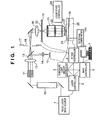
- Fig. 1 is a schematic view showing the main part of a liquid immersion exposure apparatus according to the first embodiment of the present invention.
- the liquid immersion exposure apparatus is a scanning exposure apparatus which irradiates, with a light beam emitted from a pulse laser light source, an original plate (reticle) through an illumination optical system (illumination means), reduces and projects a circuit pattern formed on the reticle, and prints, through a projection lens (projection optical system), it onto a wafer (substrate) coated with a photosensitive material while scanning the reticle and wafer.
- This apparatus is preferable in manufacturing a device such as a semiconductor device such as an IC or LSI, an image sensing device such as a CCD, or a magnetic head.
- a pulse laser light source (light source means) 1 such as an excimer laser emits pulse light.
- a beam shaping unit 10 fixes the light beam from the laser light source 1 into a predetermined illumination shape and applies it to the incident surface of a fly-eye lens 11.
- the fly-eye lens 11 comprises a plurality of microlenses and forms a plurality of secondary sources near its exit surface.
- a condenser lens 12 Koehler-illuminates an exposure slit 16 and movable slit (masking blade) 17 with the light beam from the secondary source near the light exit surface of the fly-eye lens 11.
- the light beam having illuminated the movable slit 17 illuminates a reticle 20 through a collimator lens 18.
- the movable slit 17 is optically conjugate to the reticle 20. This positional relationship allows the opening shape of the movable slit 17 to define the shape and dimensions of the illumination region of the reticle 20.
- the movable slit 17 includes, e.g., a voice coil motor (not shown) to move it in the direction of the optical axis.
- a light exposure integrator (light exposure integrating meter) 15 causes a collective lens (condenser lens) 14 to partially focus the pulse-like illumination light separated by a half mirror 13 to detect the light amount, thereby outputting the detection signal to an light exposure controller 3.
- the beam shaping unit 10, fly-eye lens 11, condenser lens 12, exposure slit 16, movable slit 17, and collimator lens 18 constitute one component of an illumination means (exposure light providing means) for providing exposure light to the reticle 20.
- a beam attenuation means (not shown) is provided in the illumination means to adjust the amount of light beam from the laser light source 1 with multiple steps.
- the reticle 20 has a circuit pattern thereon and is held by a reticle stage 19.
- a projection lens (projection optical system) 21 reduces the circuit pattern of the reticle 20 and projects it onto a wafer 26.
- the surface of the wafer 26 is coated with a resist as a photosensitive agent.
- the wafer 26 is placed on a wafer stage 25 which is three-dimensionally displaced and aligned at an arbitrary position.
- the surface of the wafer 26 is located at a position conjugate to the movable slit 17.
- An internal illuminometer 23 is formed on the wafer stage 25 and measures the amount of pulse light through the projection lens 21, as will be described later.
- the A light exposure integrator 15 can measure the light amount intensity even during exposure, it is used to estimate the integrated value of the exposure light emitted from the exposure slit 16.
- the internal illuminometer 23 is used to measure the intensity of the pulse light (in the image plane of the projection lens 21) which is transmitted through the projection lens 21 in the first stage of the exposure process and applied to the wafer 26.
- a stage driving controller (scanning means) 4 controls to move the reticle stage 19 and wafer stage 25 in directions reverse to each other at an exactly constant velocity having the same ratio as the imaging magnification used by the projection lens (projection optical system) 21.
- the light exposure controller 3 converts an electrical signal, which is photoelectrically converted by the A light exposure integrator 15, into a logical value and outputs it to a main controller 5.
- the output value is stored in a storage means in the main controller 5.
- the correlation between the measurement value (light intensity) obtained by the internal illuminometer 23 and the measurement value obtained by the light exposure integrator 15 is calculated in advance. In each exposure, the measurement value of the light exposure integrator 15 is corrected using the obtained correlation to calculate the exposure amount on the wafer.
- the internal illuminometer 23 does not measure the exposure light intensity during wafer exposure.
- a laser controller 2 outputs a trigger signal and charge voltage signal in accordance with a desired exposure amount to control the pulse energy and light-emitting interval of the laser light source 1.
- the laser controller 2 uses as parameters, an illuminance monitor signal from the light exposure controller 3, a current stage position signal from the stage controller 4, and use log information from the main controller 5.
- the main controller 5 calculates a group of parameters necessary for scanning exposure on the basis of data given by an input device 7, parameters unique to the apparatus, and the measurement data obtained by measurement means such as the light exposure integrator 15.
- the main controller 5 transmits these parameters to the laser controller 2, stage controller 4, and beam shaping unit 10.
- a liquid state controller (also called a liquid immersion mechanism) 28 supplies a liquid to the gap between the final surface of the projection lens 21 and the exposure target such as the substrate 26 or internal illuminometer 23, and recovers the liquid from the gap, thereby filling the gap with the liquid (setting a liquid immersion state).
- absolute value calibration and calibration between apparatuses according to this embodiment are executed using an external illuminometer (reference illuminometer) 24 which serves as a tool that is loaded from the outside of the apparatus and can be arranged on the imaging plane.
- an external illuminometer reference illuminometer
- Absolute value calibration and calibration between the apparatuses are executed for a reference internal illuminometer out of a plurality of internal illuminometers 23 formed on the wafer stage 25.
- the reference internal illuminometer formed on the wafer stage 25 desirably has the same angular characteristic, which causes an output variation depending on an incident angle, as that of the external illuminometer 24.
- the reference internal illuminometer further desirably has the same sensitivity characteristic which causes an output variation depending on the amount of received light.
- the sensitivity of the internal illuminometer 23 may be separately calibrated for each condition, i.e., a case in which the NA of the projection lens or the exposure amount changes between them, thus compensating the sensitivity of the internal illuminometer 23 in accordance with the conditions of the exposure amount and the NA value of the projection lens (which can be changed by an NA stop 22), which are to be changed.
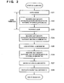
- measurement values LID, ILD, LII, ILI, LIA, and ILA are measured.
- the measurement values LID and ILD are obtained by the light exposure integrator 15 and the reference internal illuminometer, respectively, in a dried state.
- the measurement values LII and ILI are obtained by the light exposure integrator 15 and the reference internal illuminometer, respectively, in a liquid immersion state.
- the measurement values LIA and ILA are obtained by the light exposure integrator 15 and external illuminometer 24, respectively, in the dried state.
- a calibration coefficient D of the light exposure integrator 15 in liquid immersion is calculated on the basis of the above values.
- a coefficient of the reference internal illuminometer can also be calculated on the basis of the relationship between the measurement values of the light exposure integrator 15 and reference internal illuminometer.
- a liquid is supplied (step S21).
- the value LII of the light exposure integrator 15 and the value ILI of the reference internal illuminometer 23 are measured in a liquid immersion state (step S22).
- the liquid is discharged (step S23).
- the value LID of the light exposure integrator 15 and the value ILD of the reference internal illuminometer 23 are measured in a dried state (step S24).
- the external illuminometer 24 is loaded (step S25).
- the value LIA of the light exposure integrator 15 and the value ILA of the external illuminometer 24 are measured in the dried state (step S26).
- the external illuminometer 24 is unloaded (step S27).
- the external illuminometer 24 loaded from the outside of the apparatus is not set a liquid immersion state, so the measurement operation is very efficient.
- the transmittance of the liquid is then calculated on the basis of the measurement values LID and ILD obtained by the light exposure integrator 15 and the reference internal illuminometer 23, respectively, in the dried state, and LII and ILI obtained by the light exposure integrator 15 and the reference internal illuminometer 23, respectively, in the liquid immersion state.
- the calibration coefficient D in liquid immersion is calculated by multiplying the calculated liquid transmittance by the ratio of the measurement value LIA of the light exposure integrator 15 to the measurement value ILA of the external illuminometer 24, in the dried state (step S28).
- the light exposure integrator (or the reference internal illuminometer) can be calibrated according to circumstances on the basis of an output from the light exposure integrator (or the reference internal illuminometer) in liquid immersion or non-liquid immersion, an output from the external illuminometer in non-liquid immersion, and information about the transmittance of the liquid, which is measured and stored in advance.
- the data of the transmittance of the liquid which is obtained by periodical measurement and held in the exposure apparatus, can be used to compensate a short-term variation in transmittance due to the projection optical system.
- the NA of the projection lens must remain the same for measurement in both the liquid immersion state and dry state (non liquid immersion state).
- the liquid transmittance, the focus (Fo1, Fo2), and the incident angle ( ⁇ 1, ⁇ 2) to the internal illuminometer change between the liquid immersion state and the dry state.
- the liquid transmittance has already been calculated in step S28 of Fig. 2.
- the incident angle to the internal illuminometer 23 an NA higher than 1.0 attained in liquid immersion is practically impossible in the dried state. Therefore, it is difficult to always keep the same NA of the projection lens in both the states.
- angular characteristic data of the light reception sensitivity of the internal illuminometer 23 is held in advance in the exposure apparatus (e.g., a nonvolatile memory of the main controller 5).
- Fig. 4 shows an angular characteristic of the internal illuminometer.
- Fig. 4 is a graph showing the relative ratio of sensitivity which changes depending on the difference in incident angle to the internal illuminometer 23. Using this ratio, the internal illuminometer 23 is calibrated by a method of estimating an actual exposure amount on the basis of the incident angle to the NA of the projection lens and an actual light amount measured by the internal illuminometer 23.
- This calculation can be executed by, e.g., the main controller 5.
- a calibration method in consideration of deterioration characteristics of a plurality of internal illuminometer will be described next.
- accuracy deterioration characteristic data is stored in the apparatus (e.g., the nonvolatile memory of the main controller 5) for each of the plurality of internal illuminometers 23.
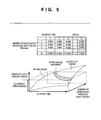
- An example of the accuracy deterioration characteristic data in Fig. 5 shows an empirical independence relationship between the output value of the internal illuminometer 23 and the elapsed time and the number of integrated light pulses received by the internal illuminometer 23 after preceding absolute value calibration and calibration between the apparatuses.
- Three states, i.e., "within a range”, “within a range (warning)", and "outside of a range” are represented depending on an allowable deterioration value.
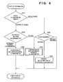
- step S31 determines whether a deterioration error falls within the allowable value by referring to the accuracy deterioration data (Fig. 5) of the internal illuminometer 23 (step S31). If the accuracy deterioration falls outside the allowable range, the internal illuminometer for use undergo absolute value calibration and calibration between the apparatuses. At this time, whether the internal illuminometer for use serves as the reference is determined (step S33). If the internal illuminometer for use serves as the reference, calibration in Fig. 2 is executed (step S35).
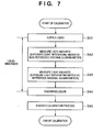
- step S34 indirect calibration in Fig. 7 is executed without using the external illuminometer 24 (step S34).
- step S31 even when the deterioration error falls within the allowable range (step S31), if it exceeds a threshold value for warning (step S32), the user is notified that the internal illuminometer 23 needs to undergo absolute value calibration and calibration between the apparatuses (step S36).
- Calculation (calculation of the calibration coefficient) and control of the process shown in Fig. 6 can be executed by, e.g., the main controller 5.
- Fig. 7 is a flowchart showing the process of calibrating the non-reference internal illuminometer.
- the calibration (calculation of the calibration coefficient) and control of the process can be executed by, e.g., the main controller 5.
- step S41 after a liquid is supplied (step S41), the light amounts of the light exposure integrator vs. non-reference internal illuminometer are measured in a liquid immersion state (step S42). Furthermore, the light amounts of the light exposure integrator vs. the reference internal illuminometer are measured (step S43). After the liquid is discharged (step S44), the measurement value of the non-reference internal illuminometer is calibrated by the measurement value of the reference internal illuminometer (step S45).
- the external illuminometer 24 is used in a dried state. This makes it possible to shorten a time required to calibrate the internal illuminometer in liquid immersion exposure.
- calibrating the plurality of internal illuminometers 23 (which do not serve as the references) in the exposure apparatus by rarely using the external illuminometer 24 makes it possible to minimize the calibration time of the internal illuminometer 23.
- the accuracy deterioration characteristic data of the internal illuminometer 23 is held in the apparatus to compensate an accuracy deterioration in accordance with factors such as a temporal change and the number of integrated received light pulses. This allows the exposure amount error to always fall within the allowable value. Holding, in the apparatus, the sensitivity characteristic data of the internal illuminometer 23 to the exposure light reception angle also makes it possible to highly accurately convert the data of the internal illuminometer having an angular characteristic into the exposure amount.
- the internal illuminometer 23 since the internal illuminometer 23 has an angular characteristic, it is difficult to set the same NA of the projection lens both in the liquid immersion state and dried state.
- calibration in consideration of the angular characteristic can be implemented as follows. As shown in Fig. 8, a movable prism 30 and zoom lens 31 are arranged on the optical path of an internal illuminometer 23 in a waterproof protection box 29. A mechanism which can change the incident angle of exposure light depending on the above positional relationship is formed to allow the exposure light to strike the internal illuminometer 23 at the same angle as the NA of the projection lens as in the dried state.
- the angle of exposure light received by the internal illuminometer 23 is adjusted using the movable prism 30 and zoom lens 31 to highly accurately execute absolute light amount calibration in the liquid immersion state.
- Accuracy deterioration characteristic data of the internal illuminometer 23 is held in advance in the exposure apparatus to control an accuracy deterioration. Therefore, even when the projection optical system is used in the liquid immersion state, an exposure amount control performance with high accuracy like in a dried state can be attained.
- Fig. 9 shows the flow of the manufacture of a microdevice (a semiconductor chip such as an IC or LSI, a liquid crystal panel, a CCD, a thin-film magnetic head, or a micromachine).
- a semiconductor device such as an IC or LSI, a liquid crystal panel, a CCD, a thin-film magnetic head, or a micromachine.
- step S1 circuit design
- step S2 exposure control data creation
- exposure control data of the exposure apparatus is created on the basis of the designed circuit pattern.
- step S3 wafer manufacture
- a wafer is manufactured using a material such as silicon.
- step S4 wafer process
- an actual circuit is formed on the wafer by lithography using the wafer and the exposure apparatus which has received the prepared exposure control data.
- Step S5 (assembly) called a post-process is the step of forming a semiconductor chip by using the wafer manufactured in step S4. This step includes processes such as assembly (dicing and bonding) and packaging (chip encapsulation).
- step S6 the semiconductor device manufactured in step S5 undergoes inspections such as an operation confirmation test and durability test. After these steps, the semiconductor device is completed and shipped (step S7).
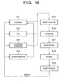
- Fig. 10 shows the detailed flow of the wafer process.
- step S11 oxidation
- step S12 CVD
- step S13 electrode formation
- step S14 ion implantation
- ions are implanted in the wafer.
- step S15 resist process
- step S16 exposure
- step S18 etching
- step S19 resist removal
Landscapes
- Physics & Mathematics (AREA)
- General Physics & Mathematics (AREA)
- Health & Medical Sciences (AREA)
- Engineering & Computer Science (AREA)
- Environmental & Geological Engineering (AREA)
- Epidemiology (AREA)
- Public Health (AREA)
- Exposure And Positioning Against Photoresist Photosensitive Materials (AREA)
- Exposure Of Semiconductors, Excluding Electron Or Ion Beam Exposure (AREA)
Applications Claiming Priority (1)
| Application Number | Priority Date | Filing Date | Title |
|---|---|---|---|
| JP2005122946A JP2006303193A (ja) | 2005-04-20 | 2005-04-20 | 露光装置、較正方法、およびデバイス製造方法 |
Publications (2)
| Publication Number | Publication Date |
|---|---|
| EP1715380A2 true EP1715380A2 (fr) | 2006-10-25 |
| EP1715380A3 EP1715380A3 (fr) | 2009-01-21 |
Family
ID=36763048
Family Applications (1)
| Application Number | Title | Priority Date | Filing Date |
|---|---|---|---|
| EP06006953A Withdrawn EP1715380A3 (fr) | 2005-04-20 | 2006-03-31 | Appareil d'exposition, procédé appliqué à l'appareil et procédé de fabrication d'un dispositif |
Country Status (4)
| Country | Link |
|---|---|
| US (1) | US7486379B2 (fr) |
| EP (1) | EP1715380A3 (fr) |
| JP (1) | JP2006303193A (fr) |
| KR (1) | KR100825932B1 (fr) |
Cited By (1)
| Publication number | Priority date | Publication date | Assignee | Title |
|---|---|---|---|---|
| WO2009050977A1 (fr) * | 2007-10-16 | 2009-04-23 | Nikon Corporation | Système optique d'éclairage, appareil d'exposition et procédé de fabrication de dispositif |
Families Citing this family (4)
| Publication number | Priority date | Publication date | Assignee | Title |
|---|---|---|---|---|
| US8253924B2 (en) | 2005-05-24 | 2012-08-28 | Nikon Corporation | Exposure method, exposure apparatus and device manufacturing method |
| JP4908948B2 (ja) * | 2006-06-30 | 2012-04-04 | キヤノン株式会社 | 露光装置およびデバイス製造方法 |
| JP4528337B2 (ja) * | 2008-03-03 | 2010-08-18 | キヤノン株式会社 | 露光装置およびデバイス製造方法 |
| TW201122564A (en) * | 2009-06-25 | 2011-07-01 | Nikon Corp | Optical element, illumination apparatus, exposure apparatus, and method for manufacturing device |
Citations (1)
| Publication number | Priority date | Publication date | Assignee | Title |
|---|---|---|---|---|
| EP1500982A1 (fr) | 2003-07-24 | 2005-01-26 | ASML Netherlands B.V. | Appareil lithographique et méthode de fabrication d'un dispositif |
Family Cites Families (9)
| Publication number | Priority date | Publication date | Assignee | Title |
|---|---|---|---|---|
| US4841132A (en) | 1986-07-21 | 1989-06-20 | Matsushita Electric Industrial Co., Ltd. | Program recording scheduling apparatus using an optical reader |
| JPS6349893A (ja) | 1986-08-19 | 1988-03-02 | Matsushita Electric Ind Co Ltd | バ−コ−ド読み取り装置 |
| JPH1092722A (ja) * | 1996-09-18 | 1998-04-10 | Nikon Corp | 露光装置 |
| US5825043A (en) * | 1996-10-07 | 1998-10-20 | Nikon Precision Inc. | Focusing and tilting adjustment system for lithography aligner, manufacturing apparatus or inspection apparatus |
| KR101548832B1 (ko) | 2003-05-28 | 2015-09-01 | 가부시키가이샤 니콘 | 노광 방법, 노광 장치, 및 디바이스 제조 방법 |
| JP5143331B2 (ja) | 2003-05-28 | 2013-02-13 | 株式会社ニコン | 露光方法及び露光装置、並びにデバイス製造方法 |
| EP1486828B1 (fr) * | 2003-06-09 | 2013-10-09 | ASML Netherlands B.V. | Appareil lithographique et méthode de fabrication d'un dispositif |
| JP2005175034A (ja) * | 2003-12-09 | 2005-06-30 | Canon Inc | 露光装置 |
| US7092072B2 (en) * | 2004-07-02 | 2006-08-15 | Asml Netherlands B.V. | Calibration apparatus and method of calibrating a radiation sensor in a lithographic apparatus |
-
2005
- 2005-04-20 JP JP2005122946A patent/JP2006303193A/ja not_active Withdrawn
-
2006
- 2006-03-31 EP EP06006953A patent/EP1715380A3/fr not_active Withdrawn
- 2006-04-06 US US11/398,586 patent/US7486379B2/en not_active Expired - Fee Related
- 2006-04-20 KR KR1020060035669A patent/KR100825932B1/ko not_active Expired - Fee Related
Patent Citations (1)
| Publication number | Priority date | Publication date | Assignee | Title |
|---|---|---|---|---|
| EP1500982A1 (fr) | 2003-07-24 | 2005-01-26 | ASML Netherlands B.V. | Appareil lithographique et méthode de fabrication d'un dispositif |
Cited By (2)
| Publication number | Priority date | Publication date | Assignee | Title |
|---|---|---|---|---|
| WO2009050977A1 (fr) * | 2007-10-16 | 2009-04-23 | Nikon Corporation | Système optique d'éclairage, appareil d'exposition et procédé de fabrication de dispositif |
| CN101681125B (zh) * | 2007-10-16 | 2013-08-21 | 株式会社尼康 | 照明光学系统、曝光装置以及元件制造方法 |
Also Published As
| Publication number | Publication date |
|---|---|
| US7486379B2 (en) | 2009-02-03 |
| KR20060110818A (ko) | 2006-10-25 |
| EP1715380A3 (fr) | 2009-01-21 |
| KR100825932B1 (ko) | 2008-04-28 |
| US20060238734A1 (en) | 2006-10-26 |
| JP2006303193A (ja) | 2006-11-02 |
Similar Documents
| Publication | Publication Date | Title |
|---|---|---|
| JP3402850B2 (ja) | 投影露光装置及びそれを用いたデバイスの製造方法 | |
| US7084982B2 (en) | Optical apparatus, measurement method, and semiconductor device manufacturing method | |
| EP1796142A1 (fr) | Dispositif de mesure des caracteristiques optiques, methode de mesure des caracteristiques optiques, dispositif d'exposition, methode d'exposition, et une methode pour fabriquer le dispositif | |
| US7760326B2 (en) | Exposure apparatus and aberration correction method | |
| US7843550B2 (en) | Projection optical system inspecting method and inspection apparatus, and a projection optical system manufacturing method | |
| US7298498B2 (en) | Optical property measuring apparatus and optical property measuring method, exposure apparatus and exposure method, and device manufacturing method | |
| JP3904034B2 (ja) | 露光装置 | |
| US9513460B2 (en) | Apparatus and methods for reducing autofocus error | |
| KR20080007383A (ko) | 노광 방법 및 노광 장치, 그리고 디바이스 제조 방법 | |
| US7486379B2 (en) | Exposure apparatus, method applied to the apparatus, and device manufacturing method | |
| EP1703329A1 (fr) | Appareil d'exposition par immersion, procédé d'exposition par immersion et procédé de fabrication d'un dispositif | |
| JP3414476B2 (ja) | 投影露光装置 | |
| JPH08162397A (ja) | 投影露光装置及びそれを用いた半導体デバイスの製造方法 | |
| US7433020B2 (en) | Apparatus having photoelectric converting element, and device manufacturing method | |
| JP4845766B2 (ja) | リソグラフィ装置、デバイス製造方法およびエネルギセンサ | |
| JP2002198281A (ja) | 照明装置及びそれを用いた露光装置 | |
| EP1548501A2 (fr) | Système laser et appareil d'exposition micro-lithographique, ainsi que méthode associée | |
| US20040184015A1 (en) | Aligner and device fabrication method | |
| JP5370708B2 (ja) | 工具物体、計測装置及び露光装置、並びに計測方法及び調整方法 | |
| US7595862B2 (en) | Exposure apparatus and method of manufacturing device | |
| JP2003014643A (ja) | 透過率測定装置、並びに露光装置 | |
| JPH11186148A (ja) | 露光装置 | |
| JPH09115802A (ja) | 露光方法及び露光装置及びそれを用いたデバイスの製造方法 | |
| JPH09205053A (ja) | センサ制御装置及びそれを用いた走査型露光装置 | |
| JP2001217182A (ja) | センサ制御装置及びそれを用いた露光装置 |
Legal Events
| Date | Code | Title | Description |
|---|---|---|---|
| PUAI | Public reference made under article 153(3) epc to a published international application that has entered the european phase |
Free format text: ORIGINAL CODE: 0009012 |
|
| AK | Designated contracting states |
Kind code of ref document: A2 Designated state(s): AT BE BG CH CY CZ DE DK EE ES FI FR GB GR HU IE IS IT LI LT LU LV MC NL PL PT RO SE SI SK TR |
|
| AX | Request for extension of the european patent |
Extension state: AL BA HR MK YU |
|
| PUAL | Search report despatched |
Free format text: ORIGINAL CODE: 0009013 |
|
| AK | Designated contracting states |
Kind code of ref document: A3 Designated state(s): AT BE BG CH CY CZ DE DK EE ES FI FR GB GR HU IE IS IT LI LT LU LV MC NL PL PT RO SE SI SK TR |
|
| AX | Request for extension of the european patent |
Extension state: AL BA HR MK YU |
|
| 17P | Request for examination filed |
Effective date: 20090721 |
|
| AKX | Designation fees paid |
Designated state(s): AT BE BG CH CY CZ DE DK EE ES FI FR GB GR HU IE IS IT LI LT LU LV MC NL PL PT RO SE SI SK TR |
|
| GRAP | Despatch of communication of intention to grant a patent |
Free format text: ORIGINAL CODE: EPIDOSNIGR1 |
|
| STAA | Information on the status of an ep patent application or granted ep patent |
Free format text: STATUS: THE APPLICATION HAS BEEN WITHDRAWN |
|
| 18W | Application withdrawn |
Effective date: 20130211 |