EP1679575A2 - Signalerfassungsvorrichtung, Frequenzerfassungsvorrichtung, Vorrichtung zur Stromverbrauchskontrolle, entsprechende Verfahren und elektronisches Gerät, das diese verwendet - Google Patents
Signalerfassungsvorrichtung, Frequenzerfassungsvorrichtung, Vorrichtung zur Stromverbrauchskontrolle, entsprechende Verfahren und elektronisches Gerät, das diese verwendet Download PDFInfo
- Publication number
- EP1679575A2 EP1679575A2 EP05009782A EP05009782A EP1679575A2 EP 1679575 A2 EP1679575 A2 EP 1679575A2 EP 05009782 A EP05009782 A EP 05009782A EP 05009782 A EP05009782 A EP 05009782A EP 1679575 A2 EP1679575 A2 EP 1679575A2
- Authority
- EP
- European Patent Office
- Prior art keywords
- signal
- detecting
- power consumption
- state
- inputted
- Prior art date
- Legal status (The legal status is an assumption and is not a legal conclusion. Google has not performed a legal analysis and makes no representation as to the accuracy of the status listed.)
- Withdrawn
Links
Images



Classifications
-
- G—PHYSICS
- G06—COMPUTING OR CALCULATING; COUNTING
- G06F—ELECTRIC DIGITAL DATA PROCESSING
- G06F1/00—Details not covered by groups G06F3/00 - G06F13/00 and G06F21/00
- G06F1/26—Power supply means, e.g. regulation thereof
- G06F1/32—Means for saving power
- G06F1/3203—Power management, i.e. event-based initiation of a power-saving mode
-
- Y—GENERAL TAGGING OF NEW TECHNOLOGICAL DEVELOPMENTS; GENERAL TAGGING OF CROSS-SECTIONAL TECHNOLOGIES SPANNING OVER SEVERAL SECTIONS OF THE IPC; TECHNICAL SUBJECTS COVERED BY FORMER USPC CROSS-REFERENCE ART COLLECTIONS [XRACs] AND DIGESTS
- Y02—TECHNOLOGIES OR APPLICATIONS FOR MITIGATION OR ADAPTATION AGAINST CLIMATE CHANGE
- Y02D—CLIMATE CHANGE MITIGATION TECHNOLOGIES IN INFORMATION AND COMMUNICATION TECHNOLOGIES [ICT], I.E. INFORMATION AND COMMUNICATION TECHNOLOGIES AIMING AT THE REDUCTION OF THEIR OWN ENERGY USE
- Y02D10/00—Energy efficient computing, e.g. low power processors, power management or thermal management
Definitions
- the present invention relates to a signal detection method, a power consumption control method, a signal detecting device and a power consumption control device that detect input of a signal to an input terminal; a frequency detection method and a frequency detecting device that detect the frequency of the signal; a signal detection method, a power consumption control method, a signal detecting device and a power consumption control device that detect whether a signal inputted to an input terminal is in a first state in which the signal repeatedly goes to a high level and a low level alternately, or in a second state in which the signal is kept at a high level or a low level and an electronic apparatus comprising the power consumption control device.
- a bias current or the like continues to flow, and therefore electric power is often wastefully consumed.
- a pre-scaler used in a PLL (Phase-Locked Loop) or the like is not operating, but a bias current continues to flow.
- a power consumption reduction signal is outputted to block the bias current or the like (see Japanese Patent Application Laid Open No. 2000-224015).
- a power consumption control device that outputs a power save signal (power consumption reduction signal) when it detects that no signal is outputted to a pre-scaler from an oscillator, an attempt is made to reduce power consumption by blocking the bias current in the pre-scaler when it is not operating.
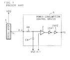
- FIG. 1 is a circuit diagram showing the essential structure of an electronic apparatus comprising a power consumption control device.
- a power consumption control device 6 is connected to an output terminal CL of an oscillator 4 which is an operation monitoring target.
- a clock signal similar to a signal supplied to a pre-scaler, not shown, is outputted from the output terminal CL.
- one of the terminals of a resistor R8 is connected via an input terminal Vin to the output terminal CL of the oscillator 4, and a capacitor C8 is connected between the other terminal of the resistor R8 and a ground terminal VGD.
- the node of the resistor R8 and capacitor C8 is connected to a non-inverted input terminal of a comparator 2.
- a reference voltage terminal Vrf is connected to an inverted input terminal of the comparator 2, and the output terminal of the comparator 2 is connected to a power save signal output terminal PS through two inverters INV1 and INV2.
- the power save signal output terminal PS can be connected, for example, to a power supply device (not shown) to stop power supply to the pre-scaler from the power supply device or reduce the supply voltage, or can be connected, for example, to a pre-scaler (not shown) to give an operation stop signal or a standby signal to the pre-scaler.
- the clock signal outputted from the CL terminal of the oscillator 4 is integrated by the resistor R8 and capacitor C8 and then outputted to the comparator 2, so when the clock signal is inputted and repeatedly going to a high state and a low state alternately, the power save signal goes high.
- the power save signal goes low.
- the power save signal goes high similarly to the input of the clock signal, and thus there is the problem that power saving cannot be achieved.
- FIG. 2 is a circuit diagram showing the essential structure of an electronic apparatus comprising other power consumption control device in which a capacitor C9 is connected between the above-described input terminal Vin and resistor R8 of the power consumption control device 8. Note that the circuit shown in FIG. 2 has the same structure as the circuit of FIG. 1, except for the capacitor C9.
- the DC component of the clock signal inputted to the input terminal Vin of the power consumption control device 8 is cut, even when the clock signal is stopped in a high state, the power save signal is low.
- the power save signal since there is no path for actively discharging the charge accumulated in the capacitor C8, it will take a long time until the power save signal goes low after the clock signal was stopped in a high state, and consequently there is the problem that power saving cannot be achieved quickly.
- the present invention has been made with the aim of solving the above problems, and it is an object of the present invention to provide a signal detection method and a signal detecting device, capable of detecting the presence or absence of an input signal by a simple structure by applying a signal inputted to an input terminal to the gates of a p-type transistor and an n-type transistor connected in series, for example, to detect a through current.
- Another object of the present invention is to provide a signal detection method and a signal detecting device, capable of detecting whether a signal inputted to an input terminal is in a first state in which the signal repeatedly goes to a high level and a low level alternately, or in a second state in which the signal is kept at a high level or a low level, by a simple structure by applying the signal to the gates of a p-type transistor and an n-type transistor connected in series, for example, to detect a through current, and determining that the signal is in the first state when the through current is detected, or determining that the signal is in the second state when the through current is not detected in a predetermined period of time.
- Still another object of the present invention is to provide a frequency detection method and a frequency detecting device, capable of detecting the frequency of a signal by a simple structure by applying a signal inputted to an input terminal to the gates of a p-type transistor and an n-type transistor connected in series, for example, to detect a through current, and detecting the frequency of the signal based on the detected through current.
- Yet another object of the present invention is to provide a power consumption control method and a power consumption control device, capable of detecting whether an operation monitoring target is operating or is stopped and outputting a power consumption reduction signal by a simple structure by applying a signal inputted to an input terminal to the gates of a p-type transistor and an n-type transistor connected in series, for example, to detect a through current flowing through the p-type transistor and n-type transistor, and outputting a power consumption reduction signal when the through current is not detected in a predetermined period of time.
- a further object of the present invention is to provide a power consumption control method and a power consumption control device, capable of detecting an operation state of an operation monitoring target and outputting a power consumption reduction signal according to the operation state by a simple structure by applying a signal inputted to an input terminal to the gates of a p-type transistor and an n-type transistor connected in series, for example, to detect a through current flowing through the p-type transistor and n-type transistor, and determining that the signal is in a first state in which the signal repeatedly goes to a high level and a low level alternately when the through current is detected, or determining that the signal is in a second state in which the signal is kept at a high level or a low level when the through current is not detected in a predetermined period of time.
- a further object of the present invention is to provide an electronic apparatus capable of executing a power supply stopping process or a power supply reducing process, according to a power consumption reduction signal outputted from the power consumption control device.
- a signal detection method is a signal detection method for detecting input of a signal to an input terminal, and characterized by comprising: detecting a through current flowing through a circuit to which the signal is inputted; and detecting input of the signal, based on whether or not the through current flowed through the circuit.
- a signal detection method is a signal detection method for detecting whether a signal inputted to an input terminal is in a first state in which the signal repeatedly goes to a high level and a low level alternately, or in a second state in which the signal is kept at a high level or a low level, and characterized by comprising: detecting a through current flowing through a circuit to which the signal is inputted; determining that the signal is in the first state when the through current is detected; and determining that the signal is in the second state when the through current is not detected in a predetermined period of time.
- a signal detection method is characterized in that the circuit includes a p-type transistor and an n-type transistor with gates to which the signal is inputted.
- a frequency detection method is a frequency detection method for detecting a frequency of a signal inputted to an input terminal, and characterized by comprising: detecting a through current flowing through a circuit to which the signal is inputted; and detecting the frequency based on the detected through current.
- a frequency detection method is characterized in that the circuit includes a p-type transistor and an n-type transistor with gates to which the signal is inputted.
- a power consumption control method is a power consumption control method comprising detecting input of a signal outputted from an operation monitoring target to an input terminal, and outputting a power consumption reduction signal when the signal is not detected in a predetermined period of time, and characterized by comprising: detecting a through current flowing through a circuit to which the signal is inputted; and outputting the power consumption reduction signal when the through current is not detected in a predetermined period of time.
- a power consumption control method is a power consumption control method comprising determining whether a signal outputted from an operation monitoring target and inputted to an input terminal is in a first state in which the signal repeatedly goes to a high level and a low level alternately, or in a second state in which the signal is kept at a high level or a low level, and outputting a power consumption reduction signal when the signal is determined as being in the second state, and characterized by comprising: detecting a through current flowing through a circuit to which the signal is inputted; determining that the signal is in the first state when the through current is detected; and determining that the signal is in the second state when the through current is not detected in a predetermined period of time.
- a signal detecting device is a signal detecting device for detecting input of a signal to an input terminal, and characterized by comprising detecting means for detecting a through current flowing through a circuit to which the signal is inputted, wherein the signal detecting device detects input of the signal, based on whether or not the through current flowed through the circuit.
- a signal detecting device is a signal detecting device for detecting whether a signal inputted to an input terminal is in a first state in which the signal repeatedly goes to a high level and a low level alternately, or in a second state in which the signal is kept at a high level or a low level, and characterized by comprising detecting means for detecting a through current flowing through a circuit to which the signal is inputted, wherein the signal detecting device determines the signal is in the first state when the detecting means detects the through current, and determines the signal is in the second state when the detecting means does not detect the through current in a predetermined period of time.
- a signal detecting device is characterized in that the circuit includes a p-type transistor and an n-type transistor with gates to which the signal is inputted.
- a frequency detecting device is a frequency detecting device for detecting a frequency of a signal inputted to an input terminal, and characterized by comprising detecting means for detecting a through current flowing through a circuit to which the signal is inputted, wherein the frequency detecting device detects the frequency, based on the through current detected by the detecting means.
- a frequency detecting device is characterized in that the circuit includes a p-type transistor and an n-type transistor with gates to which the signal is inputted.
- a power consumption control device is a power consumption control device for detecting input of a signal outputted from an operation monitoring target to an input terminal, and outputting a power consumption reduction signal when the signal is not detected in a predetermined period of time, and characterized by comprising detecting means for detecting a through current flowing through a circuit to which the signal is inputted, wherein the power consumption control device outputs the power consumption reduction signal when the through current is not detected in a predetermined period of time.
- a power consumption control device is a power consumption control device for determining whether a signal outputted from an operation monitoring target and inputted to an input terminal is in a first state in which the signal repeatedly goes to a high level and a low level alternately, or in a second state in which the signal is kept at a high level or a low level, and outputting a power consumption reduction signal when the signal is determined as being in the second state, and characterized by comprising detecting means for detecting a through current flowing through a circuit to which the signal is inputted, wherein the power consumption control device determines the signal is in the first state when the detecting means detects the through current, and determines the signal is in the second state when the detecting means does not detect the through current in a predetermined period of time.
- An electronic apparatus is characterized by comprising: the power consumption control device; a device as an operation monitoring target, which outputs a signal to the power consumption control device when it is operating; and a power supply control device for executing a power supply stopping process or a power supply reducing process for the operation monitoring target, according to the power consumption reduction signal outputted from the power consumption control device.
- An electronic apparatus is characterized by comprising: the power consumption control device; a device as an operation monitoring target, which outputs a signal to the power consumption control device, causes the signal to be in a first state in which the signal repeatedly goes to a high level and a low level alternately when it is operating, and causes the signal to be in a second state in which the signal is kept at a high level or a low level when it is not operating; and a power supply control device for executing a power supply stopping process or a power supply reducing process for the operation monitoring target, according to the power consumption reduction signal outputted from the power consumption control device.
- a signal inputted to the input terminal is applied to the gates of a p-type transistor and an n-type transistor connected in series, such as CMOS, for example, to detect a through current flowing through the p-type transistor and n-type transistor. Since the through current is generated at an intermediate potential between potentials at which ON/OFF of the p-type transistor and n-type transistor is switched, it is generated when the signal switches to a low level from a high level, or switches to a high level from a low level. Therefore, the presence or absence of an input signal can be detected based on the presence or absence of the through current. Moreover, since the through current is almost proportional to the number of times of ON/OFF switching of the input signal, the frequency of the input signal can be detected based on the through current.
- a signal inputted to the input terminal is applied to the gates of a p-type transistor and an n-type transistor connected in series, such as CMOS, for example, to detect a through current flowing through the p-type transistor and n-type transistor, and when the through current is detected, the signal is determined as being in the first state in which the signal repeatedly goes to a high level and a low level alternately, while when the through current is not detected in a predetermined period of time, the signal is determined as being in the second state in which the signal is kept at a high level or a low level.
- CMOS complementary metal-oxide
- the through current is generated at an intermediate potential between potentials at which ON/OFF of the p-type transistor and n-type transistor is switched, it is generated when the signal switches to a low level from a high level, or switches to a high level from a low level. Therefore, based on the presence or absence of the through current, it is possible to detect whether the signal is switched between high level and low level (the first state), or not (the second state). Moreover, even when the signal is kept at a high level or a low level, it is possible to detect the second state without problem.
- a signal inputted to the input terminal is applied to the gates of a p-type transistor and an n-type transistor connected in series, such as CMOS, for example, to detect a through current flowing through the p-type transistor and n-type transistor, and when the though current is not detected in a predetermined period of time, a power consumption reduction signal is outputted. Since the through current is generated at an intermediate potential between potentials at which ON/OFF of the p-type transistor and n-type transistor is switched, it is generated when the signal switches to a low level from a high level, or switches to a high level from a low level.
- the through current is almost proportional to the number of times of ON/OFF switching of the input signal, the frequency of the input signal can be detected based on the through current.
- a signal inputted to the input terminal is applied to the gates of a p-type transistor and an n-type transistor connected in series, such as CMOS, for example, to detect a through current flowing through the p-type transistor and n-type transistor, and when the through current is detected, the signal is determined as being in the first state in which the signal repeatedly goes to high level and low level alternately, while when the through current is not detected in a predetermined period of time, the signal is determined as being in the second state in which the signal is kept at a high level or a low level.
- the through current is generated at an intermediate potential between potentials at which ON/OFF of the p-type transistor and n-type transistor is switched, it is generated when the signal switches to a low level from a high level, or switches to a high level from a low level. Therefore, based on the presence or absence of the through current, it is possible to detect whether the signal is switched between high level and low level (the first state), or not (the second state), and it is possible to detect an operation state of the operation monitoring target (for example, the first state indicates that the apparatus is operating, and the second state indicates that the apparatus is stopped). Moreover, even when the signal is kept at a high level or a low level, it is possible to detect the second state without problem.
- the present invention by executing a power supply stopping process or a power supply reducing process according to a power consumption reduction signal outputted from the power consumption control device, it is possible to reduce power consumption of the electronic apparatus.
- FIG. 3 is a circuit diagram showing the essential structure of an electronic apparatus comprising a power consumption control device according to the present invention.
- the electronic apparatus comprises an oscillator 4 which is an operation monitoring target, and a power consumption control device 12.
- the power consumption control device 12 comprises a signal detecting section 10 (signal detecting device or a signal state determining device), a comparator 2, and inverters INV1 and INV2.
- the oscillator 4 has an output terminal CL for outputting a clock signal (pulse signal) similar to a signal to be supplied to a pre-scaler (not shown). Moreover, the oscillator 4 is connected to a voltage terminal VDD.
- the signal detecting section 10 of the power consumption control device 12 has a p-type transistor M1, a p-type transistor M2 and an n-type transistor M3 connected in series from the higher potential side between the voltage terminal VDD and ground terminal VGD. More specifically, the source of the transistor M1 is connected to the voltage terminal VDD, the source of the transistor M2 is connected to the drain of the transistor M1, the drain of the transistor M2 is connected to the drain of the transistor M3, and the source of the transistor M3 is connected to the ground terminal VGD. Further, in parallel with these transistors, a p-type transistor M0 and a resistor R1 are connected in series from the higher potential side, and a capacitor C1 is connected to the resistor R1 in parallel.
- the source of the transistor M0 is connected to the voltage terminal VDD, and the drain of the transistor M0 is connected to the resistor R1 and capacitor C1.
- the gates of the transistors M0 and M1 are both connected between the transistor M1 and the transistor M2.
- the gates of the transistors M2 and M3 are both connected to the output terminal CL of the oscillator 4 through an input terminal Vin.
- the transistors M0, M1, resistors R1 and capacitor C1 act as detecting means for detecting a through current flowing through the p-type transistor M2 and n-type transistor M3 connected in series.
- An output terminal Vout between the transistor M0 and resistor R1 of the signal detecting section 10 is connected to the non-inverted input terminal of the comparator 2 of the power consumption control device 12. Moreover, a reference voltage terminal Vrf is connected to the inverted input terminal of the comparator 2, and the output terminal of the comparator 2 is connected to a power save signal output terminal PS through the two inverters INV1 and INV2.
- the power save signal output terminal PS can be connected, for example, to a power supply control device (not shown) and give a power save signal (power consumption reduction signal) to the power supply control device so as to stop power supply to the pre-scaler (power supply stopping process) or reduce the supply voltage (power supply reducing process), or can be connected, for example, to a power supply control device in the pre-scaler and give a power save signal to the power supply control device so as to stop operation (power supply stopping process) or cause the power supply to stand by (power supply reducing process).
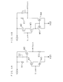
- FIG. 4A, FIG. 4B and FIG. 5 are views for explaining a through current that flows through the transistors M2 and M3 during ON/OFF switching.
- FIG. 4A is a connection diagram of the transistors M2 and M3
- FIG. 4B is a characteristic view showing the voltage of clock signal and the through current flowing through the transistors M2 and M3
- FIG. 5 is a timing chart of the clock signal and the through current.
- the signal detecting section 10 can detect the presence or absence of an input clock signal (pulse signal) irrespective of the stopped state. Moreover, the signal detecting section 10 can determine whether the input signal is in a first state in which the signal repeatedly goes to high and low alternately, or in a second state in which the input signal is stopped at a high or low level.
- FIG. 6A and FIG. 6B are circuit diagrams showing another example of the structure of the signal detecting section.
- FIG. 6A it may be possible to replace a resistor R2 for the transistor M1 shown in FIG. 3, remove the capacitor C1 and connect a capacitor C2 to the resistor R2 in parallel, or as shown in FIG. 6B, it may be possible to reverse the positive and negative polarities from those shown in FIG. 3.
- the signal detecting section (signal detecting device or signal state determining device) 10 is not limited to a power consumption control device, and can be applied to an arbitrary apparatus for detecting the presence or absence of an input signal, or determining the state of an input signal. Besides, as shown in FIG. 5, since a through current is generated during the rise or fall of a clock signal, it may also be possible to detect the frequency of the clock signal based on the through current. The detection of the frequency can be carried out based on the average voltage of the through current I shown in FIG. 5, and, for example, since the voltage at the output terminal Vout of the signal detecting section 10 shown in FIG.
- FIG. 7 is a circuit diagram showing still another example of the structure of the signal detecting section. In FIG. 7, a low-pass filter is added in the front stage of the output terminal Vout of the circuit shown in FIG. 3. Moreover, it may also be possible to use the detected frequency for the control of power consumption so that when the detected frequency is high, the apparatus is operated in a normal power mode, while when the detected frequency is low, the apparatus is operated in a power save mode.
- the present invention it is possible to detect the presence or absence of an input signal to a circuit by a simple structure, based on the presence or absence of a through current flowing in the circuit. Moreover, it is possible to detect the frequency of the input signal by a simple structure, based on the through current. In addition, according to the present invention, whether or not the input signal to the circuit is switched between high level and low level can be detected by a simple structure, based on the presence or absence of a through current flowing in the circuit.
- the present invention it is possible to detect whether an operation monitoring target is operating or stopped by a simple structure, based on the presence or absence of a through current flowing in the circuit, and it is possible to output a power consumption reduction signal according to the detection result. Moreover, it is possible to reduce power consumption of the electronic apparatus by executing a power supply stopping process or a power supply reducing process according to the power consumption reduction signal.
Landscapes
- Engineering & Computer Science (AREA)
- Theoretical Computer Science (AREA)
- Physics & Mathematics (AREA)
- General Engineering & Computer Science (AREA)
- General Physics & Mathematics (AREA)
- Manipulation Of Pulses (AREA)
- Power Sources (AREA)
- Electronic Switches (AREA)
- Logic Circuits (AREA)
- Electromechanical Clocks (AREA)
- Dc-Dc Converters (AREA)
Applications Claiming Priority (1)
| Application Number | Priority Date | Filing Date | Title |
|---|---|---|---|
| JP2005004532A JP4178279B2 (ja) | 2005-01-11 | 2005-01-11 | 信号検出方法、消費電力制御方法、信号検出装置及び消費電力制御装置 |
Publications (2)
| Publication Number | Publication Date |
|---|---|
| EP1679575A2 true EP1679575A2 (de) | 2006-07-12 |
| EP1679575A3 EP1679575A3 (de) | 2008-10-01 |
Family
ID=34936140
Family Applications (1)
| Application Number | Title | Priority Date | Filing Date |
|---|---|---|---|
| EP05009782A Withdrawn EP1679575A3 (de) | 2005-01-11 | 2005-05-04 | Signalerfassungsvorrichtung, Frequenzerfassungsvorrichtung, Vorrichtung zur Stromverbrauchskontrolle, entsprechende Verfahren und elektronisches Gerät, das diese verwendet |
Country Status (4)
| Country | Link |
|---|---|
| US (1) | US7373531B2 (de) |
| EP (1) | EP1679575A3 (de) |
| JP (1) | JP4178279B2 (de) |
| TW (1) | TWI311008B (de) |
Families Citing this family (6)
| Publication number | Priority date | Publication date | Assignee | Title |
|---|---|---|---|---|
| CN100543634C (zh) * | 2005-12-30 | 2009-09-23 | 鸿富锦精密工业(深圳)有限公司 | 超频控制电路 |
| US7750684B2 (en) | 2008-04-18 | 2010-07-06 | Nanya Technology Corp. | Power-on detection circuit for detecting minimum operational frequency |
| JP5262996B2 (ja) * | 2009-05-26 | 2013-08-14 | 富士通セミコンダクター株式会社 | 論理シミュレーション装置、方法、及びプログラム |
| JP4775516B1 (ja) | 2011-03-14 | 2011-09-21 | オムロン株式会社 | 制御装置、制御方法、プログラム、記録媒体 |
| JP5888019B2 (ja) | 2011-12-12 | 2016-03-16 | オムロン株式会社 | 制御装置、制御方法、プログラムおよび記録媒体 |
| JP7311095B2 (ja) * | 2020-10-29 | 2023-07-19 | 東芝情報システム株式会社 | アナログニューロン演算器及びその電力制御方法 |
Family Cites Families (16)
| Publication number | Priority date | Publication date | Assignee | Title |
|---|---|---|---|---|
| JPS62106815A (ja) | 1985-10-31 | 1987-05-18 | Kanai Hiroyuki | 難燃性エア−フイルタ− |
| JPH04130770A (ja) * | 1990-09-21 | 1992-05-01 | Mitsubishi Electric Corp | 半導体集積回路 |
| JPH04335297A (ja) * | 1991-05-09 | 1992-11-24 | Mitsubishi Electric Corp | 半導体集積回路装置のための入力バッファ回路 |
| JP2567172B2 (ja) * | 1992-01-09 | 1996-12-25 | 株式会社東芝 | 半導体回路の出力段に配置される出力回路 |
| US6008686A (en) * | 1997-06-24 | 1999-12-28 | Advantest Corp. | Power consumption control circuit for CMOS circuit |
| JP3367441B2 (ja) | 1999-01-28 | 2003-01-14 | 日本電気株式会社 | クロック停止検出回路及びこれを備えた半導体集積回路装置 |
| AU2001234551A1 (en) * | 2000-01-28 | 2001-08-07 | Semtech New York Corporation | Pointing device with z-axis functionality and reduced component count |
| US6668334B1 (en) * | 2000-06-27 | 2003-12-23 | Lucent Technologies Inc. | Apparatus for detecting clock failure within a fixed number of cycles of the clock |
| US6737892B2 (en) * | 2000-12-18 | 2004-05-18 | Sun Microsystems, Inc. | Method and apparatus for detecting valid clock signals at a clock receiver circuit |
| JP2003066071A (ja) * | 2001-08-23 | 2003-03-05 | Yokogawa Electric Corp | 電源周波数検出回路 |
| US6981161B2 (en) * | 2001-09-12 | 2005-12-27 | Apple Computer, Inc. | Method and apparatus for changing a digital processing system power consumption state by sensing peripheral power consumption |
| TW200416522A (en) * | 2003-02-25 | 2004-09-01 | Asustek Comp Inc | Portable computer carrying desktop computer processor and power management method thereof |
| US6765433B1 (en) * | 2003-03-20 | 2004-07-20 | Atmel Corporation | Low power implementation for input signals of integrated circuits |
| US6798372B1 (en) * | 2003-04-01 | 2004-09-28 | Maxim Integrated Products, Inc. | Switched-capacitor frequency-to-current converter |
| JP2004318748A (ja) * | 2003-04-21 | 2004-11-11 | Seiko Epson Corp | クロック信号検出回路及びそれを用いた半導体集積回路 |
| US7227411B2 (en) * | 2003-06-17 | 2007-06-05 | Broadcom Corporation | Apparatus for a differential self-biasing CMOS amplifier |
-
2005
- 2005-01-11 JP JP2005004532A patent/JP4178279B2/ja not_active Expired - Fee Related
- 2005-05-04 EP EP05009782A patent/EP1679575A3/de not_active Withdrawn
- 2005-05-05 US US11/122,123 patent/US7373531B2/en not_active Expired - Lifetime
- 2005-05-09 TW TW094114883A patent/TWI311008B/zh not_active IP Right Cessation
Also Published As
| Publication number | Publication date |
|---|---|
| JP4178279B2 (ja) | 2008-11-12 |
| EP1679575A3 (de) | 2008-10-01 |
| TWI311008B (en) | 2009-06-11 |
| US20060156044A1 (en) | 2006-07-13 |
| JP2006197038A (ja) | 2006-07-27 |
| US7373531B2 (en) | 2008-05-13 |
| TW200625814A (en) | 2006-07-16 |
Similar Documents
| Publication | Publication Date | Title |
|---|---|---|
| US7602222B2 (en) | Power up circuit with low power sleep mode operation | |
| US10164572B2 (en) | Method of monitoring clock and oscillator module thereof | |
| US8710804B2 (en) | Discharge circuit and method | |
| US8098057B2 (en) | Constant voltage circuit including supply unit having plural current sources | |
| US7372289B2 (en) | Semiconductor integrated circuit device and power supply voltage monitor system employing it | |
| US10401399B2 (en) | Low-power voltage detection circuit | |
| JP2010028424A (ja) | リセット信号生成回路 | |
| JP2010166110A (ja) | 電圧検出回路 | |
| CN107342680B (zh) | Dcdc转换器 | |
| EP3274728B1 (de) | Skalierbarer regeldifferenzdetektor eines gleichrichters mit mehreren eingängen | |
| EP2847868B1 (de) | Auf inverter und schaltkondensator basierender rauschunterdrückungsdetektor und verfahren | |
| EP1679575A2 (de) | Signalerfassungsvorrichtung, Frequenzerfassungsvorrichtung, Vorrichtung zur Stromverbrauchskontrolle, entsprechende Verfahren und elektronisches Gerät, das diese verwendet | |
| CN100568728C (zh) | 一种时钟信号检测电路 | |
| US8977869B2 (en) | Method and system for controlling power of an IC chip based on reception of signal pulse from a neighboring chip | |
| US9166468B2 (en) | Voltage regulator circuit with soft-start function | |
| KR100605452B1 (ko) | 발진 검지 회로 | |
| JP2009053984A (ja) | データ処理装置、電源電圧生成回路及びその電源電圧生成方法 | |
| JP2004070813A (ja) | 半導体集積回路 | |
| USRE42334E1 (en) | Smoothing circuit employing charging circuit intermittently charging when input voltage is higher relatively than terminal voltage and discharging circuit intermittently releasing discharging current when terminal voltage is higher relatively than input voltage | |
| CN1315259C (zh) | 电压比较器 | |
| KR100634428B1 (ko) | 전원전압 레벨 디텍터 및 그를 포함하는 파워 온 리셋 회로 | |
| JP5350995B2 (ja) | 半導体集積回路 | |
| JP2002100973A (ja) | パワーオンリセット回路 | |
| KR102076952B1 (ko) | 발진 정지 검출 회로 및 전자 기기 | |
| JP2005136950A (ja) | Cmos出力バッファ回路 |
Legal Events
| Date | Code | Title | Description |
|---|---|---|---|
| PUAI | Public reference made under article 153(3) epc to a published international application that has entered the european phase |
Free format text: ORIGINAL CODE: 0009012 |
|
| AK | Designated contracting states |
Kind code of ref document: A2 Designated state(s): AT BE BG CH CY CZ DE DK EE ES FI FR GB GR HU IE IS IT LI LT LU MC NL PL PT RO SE SI SK TR |
|
| AX | Request for extension of the european patent |
Extension state: AL BA HR LV MK YU |
|
| PUAL | Search report despatched |
Free format text: ORIGINAL CODE: 0009013 |
|
| AK | Designated contracting states |
Kind code of ref document: A3 Designated state(s): AT BE BG CH CY CZ DE DK EE ES FI FR GB GR HU IE IS IT LI LT LU MC NL PL PT RO SE SI SK TR |
|
| AX | Request for extension of the european patent |
Extension state: AL BA HR LV MK YU |
|
| RTI1 | Title (correction) |
Free format text: SIGNAL DETECTION DEVICE, FREQUENCY DETECTION DEVICE, POWER CONSUMPTION CONTROL DEVICE, CORRESPONDING METHODS AND ELECTRONIC APPARATUS USING THE SAME |
|
| RAP1 | Party data changed (applicant data changed or rights of an application transferred) |
Owner name: FUJITSU MICROELECTRONICS LIMITED |
|
| 17P | Request for examination filed |
Effective date: 20090313 |
|
| AKX | Designation fees paid |
Designated state(s): DE FR |
|
| RAP1 | Party data changed (applicant data changed or rights of an application transferred) |
Owner name: FUJITSU SEMICONDUCTOR LIMITED |
|
| RAP1 | Party data changed (applicant data changed or rights of an application transferred) |
Owner name: SPANSION LLC |
|
| RAP1 | Party data changed (applicant data changed or rights of an application transferred) |
Owner name: CYPRESS SEMICONDUCTOR CORPORATION |
|
| STAA | Information on the status of an ep patent application or granted ep patent |
Free format text: STATUS: THE APPLICATION IS DEEMED TO BE WITHDRAWN |
|
| 18D | Application deemed to be withdrawn |
Effective date: 20161201 |