EP1677371A1 - Zweiteiliger Widerstandsheizer für Phasenwechselspeicher und Herstellungsmethode - Google Patents
Zweiteiliger Widerstandsheizer für Phasenwechselspeicher und Herstellungsmethode Download PDFInfo
- Publication number
- EP1677371A1 EP1677371A1 EP04107070A EP04107070A EP1677371A1 EP 1677371 A1 EP1677371 A1 EP 1677371A1 EP 04107070 A EP04107070 A EP 04107070A EP 04107070 A EP04107070 A EP 04107070A EP 1677371 A1 EP1677371 A1 EP 1677371A1
- Authority
- EP
- European Patent Office
- Prior art keywords
- heater
- phase change
- memory
- pore
- resistance
- Prior art date
- Legal status (The legal status is an assumption and is not a legal conclusion. Google has not performed a legal analysis and makes no representation as to the accuracy of the status listed.)
- Withdrawn
Links
- 238000004519 manufacturing process Methods 0.000 title claims description 6
- 230000009977 dual effect Effects 0.000 title abstract description 5
- 239000000463 material Substances 0.000 claims abstract description 79
- 239000012782 phase change material Substances 0.000 claims abstract description 15
- 238000000151 deposition Methods 0.000 claims abstract description 4
- 150000004770 chalcogenides Chemical class 0.000 claims description 15
- 238000000034 method Methods 0.000 claims description 14
- 239000011148 porous material Substances 0.000 claims description 13
- 125000006850 spacer group Chemical group 0.000 claims description 10
- 229910052581 Si3N4 Inorganic materials 0.000 claims description 8
- NRTOMJZYCJJWKI-UHFFFAOYSA-N Titanium nitride Chemical compound [Ti]#N NRTOMJZYCJJWKI-UHFFFAOYSA-N 0.000 claims description 7
- UGACIEPFGXRWCH-UHFFFAOYSA-N [Si].[Ti] Chemical compound [Si].[Ti] UGACIEPFGXRWCH-UHFFFAOYSA-N 0.000 claims description 7
- XUIMIQQOPSSXEZ-UHFFFAOYSA-N Silicon Chemical compound [Si] XUIMIQQOPSSXEZ-UHFFFAOYSA-N 0.000 claims description 4
- QVGXLLKOCUKJST-UHFFFAOYSA-N atomic oxygen Chemical compound [O] QVGXLLKOCUKJST-UHFFFAOYSA-N 0.000 claims description 3
- 229910052760 oxygen Inorganic materials 0.000 claims description 3
- 239000001301 oxygen Substances 0.000 claims description 3
- 229910052710 silicon Inorganic materials 0.000 claims description 3
- 239000010703 silicon Substances 0.000 claims description 3
- 125000004430 oxygen atom Chemical group O* 0.000 claims 1
- 238000002513 implantation Methods 0.000 abstract description 3
- 239000010410 layer Substances 0.000 description 31
- 239000007943 implant Substances 0.000 description 6
- 150000004767 nitrides Chemical class 0.000 description 6
- 239000011669 selenium Substances 0.000 description 6
- 239000004020 conductor Substances 0.000 description 5
- 239000000203 mixture Substances 0.000 description 4
- BUGBHKTXTAQXES-UHFFFAOYSA-N Selenium Chemical compound [Se] BUGBHKTXTAQXES-UHFFFAOYSA-N 0.000 description 3
- NINIDFKCEFEMDL-UHFFFAOYSA-N Sulfur Chemical compound [S] NINIDFKCEFEMDL-UHFFFAOYSA-N 0.000 description 3
- 229910045601 alloy Inorganic materials 0.000 description 3
- 239000000956 alloy Substances 0.000 description 3
- 238000010438 heat treatment Methods 0.000 description 3
- 239000011229 interlayer Substances 0.000 description 3
- 238000002161 passivation Methods 0.000 description 3
- 229910052711 selenium Inorganic materials 0.000 description 3
- 229910052717 sulfur Inorganic materials 0.000 description 3
- 239000011593 sulfur Substances 0.000 description 3
- 230000015572 biosynthetic process Effects 0.000 description 2
- 230000008021 deposition Effects 0.000 description 2
- 238000010586 diagram Methods 0.000 description 2
- 230000005684 electric field Effects 0.000 description 2
- 229910052732 germanium Inorganic materials 0.000 description 2
- 239000003292 glue Substances 0.000 description 2
- 238000005468 ion implantation Methods 0.000 description 2
- 239000000758 substrate Substances 0.000 description 2
- 229910052714 tellurium Inorganic materials 0.000 description 2
- PORWMNRCUJJQNO-UHFFFAOYSA-N tellurium atom Chemical compound [Te] PORWMNRCUJJQNO-UHFFFAOYSA-N 0.000 description 2
- 239000010409 thin film Substances 0.000 description 2
- 239000010936 titanium Substances 0.000 description 2
- 229910000967 As alloy Inorganic materials 0.000 description 1
- OKTJSMMVPCPJKN-UHFFFAOYSA-N Carbon Chemical compound [C] OKTJSMMVPCPJKN-UHFFFAOYSA-N 0.000 description 1
- RTAQQCXQSZGOHL-UHFFFAOYSA-N Titanium Chemical compound [Ti] RTAQQCXQSZGOHL-UHFFFAOYSA-N 0.000 description 1
- UQZIWOQVLUASCR-UHFFFAOYSA-N alumane;titanium Chemical compound [AlH3].[Ti] UQZIWOQVLUASCR-UHFFFAOYSA-N 0.000 description 1
- 229910052787 antimony Inorganic materials 0.000 description 1
- WATWJIUSRGPENY-UHFFFAOYSA-N antimony atom Chemical compound [Sb] WATWJIUSRGPENY-UHFFFAOYSA-N 0.000 description 1
- 229910052785 arsenic Inorganic materials 0.000 description 1
- 229910052799 carbon Inorganic materials 0.000 description 1
- 230000001413 cellular effect Effects 0.000 description 1
- 238000004891 communication Methods 0.000 description 1
- 239000000470 constituent Substances 0.000 description 1
- 238000007796 conventional method Methods 0.000 description 1
- 238000002425 crystallisation Methods 0.000 description 1
- 230000008025 crystallization Effects 0.000 description 1
- 230000032798 delamination Effects 0.000 description 1
- 238000001312 dry etching Methods 0.000 description 1
- 238000005530 etching Methods 0.000 description 1
- 239000010408 film Substances 0.000 description 1
- GNPVGFCGXDBREM-UHFFFAOYSA-N germanium atom Chemical compound [Ge] GNPVGFCGXDBREM-UHFFFAOYSA-N 0.000 description 1
- -1 i.e. Substances 0.000 description 1
- 238000002955 isolation Methods 0.000 description 1
- 238000012986 modification Methods 0.000 description 1
- 230000004048 modification Effects 0.000 description 1
- 230000000737 periodic effect Effects 0.000 description 1
- 238000009832 plasma treatment Methods 0.000 description 1
- 229910021420 polycrystalline silicon Inorganic materials 0.000 description 1
- 238000012545 processing Methods 0.000 description 1
- 230000004044 response Effects 0.000 description 1
- 230000000717 retained effect Effects 0.000 description 1
- HBMJWWWQQXIZIP-UHFFFAOYSA-N silicon carbide Chemical compound [Si+]#[C-] HBMJWWWQQXIZIP-UHFFFAOYSA-N 0.000 description 1
- HQVNEWCFYHHQES-UHFFFAOYSA-N silicon nitride Chemical compound N12[Si]34N5[Si]62N3[Si]51N64 HQVNEWCFYHHQES-UHFFFAOYSA-N 0.000 description 1
- 238000001228 spectrum Methods 0.000 description 1
- 239000007858 starting material Substances 0.000 description 1
- 239000002344 surface layer Substances 0.000 description 1
- 239000003826 tablet Substances 0.000 description 1
- MZLGASXMSKOWSE-UHFFFAOYSA-N tantalum nitride Chemical compound [Ta]#N MZLGASXMSKOWSE-UHFFFAOYSA-N 0.000 description 1
- 229910052719 titanium Inorganic materials 0.000 description 1
- MAKDTFFYCIMFQP-UHFFFAOYSA-N titanium tungsten Chemical compound [Ti].[W] MAKDTFFYCIMFQP-UHFFFAOYSA-N 0.000 description 1
- 238000001039 wet etching Methods 0.000 description 1
Images


Classifications
-
- H—ELECTRICITY
- H10—SEMICONDUCTOR DEVICES; ELECTRIC SOLID-STATE DEVICES NOT OTHERWISE PROVIDED FOR
- H10B—ELECTRONIC MEMORY DEVICES
- H10B63/00—Resistance change memory devices, e.g. resistive RAM [ReRAM] devices
- H10B63/20—Resistance change memory devices, e.g. resistive RAM [ReRAM] devices comprising selection components having two electrodes, e.g. diodes
- H10B63/24—Resistance change memory devices, e.g. resistive RAM [ReRAM] devices comprising selection components having two electrodes, e.g. diodes of the Ovonic threshold switching type
-
- H—ELECTRICITY
- H10—SEMICONDUCTOR DEVICES; ELECTRIC SOLID-STATE DEVICES NOT OTHERWISE PROVIDED FOR
- H10N—ELECTRIC SOLID-STATE DEVICES NOT OTHERWISE PROVIDED FOR
- H10N70/00—Solid-state devices having no potential barriers, and specially adapted for rectifying, amplifying, oscillating or switching
- H10N70/011—Manufacture or treatment of multistable switching devices
- H10N70/061—Shaping switching materials
- H10N70/066—Shaping switching materials by filling of openings, e.g. damascene method
-
- H—ELECTRICITY
- H10—SEMICONDUCTOR DEVICES; ELECTRIC SOLID-STATE DEVICES NOT OTHERWISE PROVIDED FOR
- H10N—ELECTRIC SOLID-STATE DEVICES NOT OTHERWISE PROVIDED FOR
- H10N70/00—Solid-state devices having no potential barriers, and specially adapted for rectifying, amplifying, oscillating or switching
- H10N70/20—Multistable switching devices, e.g. memristors
- H10N70/231—Multistable switching devices, e.g. memristors based on solid-state phase change, e.g. between amorphous and crystalline phases, Ovshinsky effect
-
- H—ELECTRICITY
- H10—SEMICONDUCTOR DEVICES; ELECTRIC SOLID-STATE DEVICES NOT OTHERWISE PROVIDED FOR
- H10N—ELECTRIC SOLID-STATE DEVICES NOT OTHERWISE PROVIDED FOR
- H10N70/00—Solid-state devices having no potential barriers, and specially adapted for rectifying, amplifying, oscillating or switching
- H10N70/801—Constructional details of multistable switching devices
- H10N70/821—Device geometry
- H10N70/826—Device geometry adapted for essentially vertical current flow, e.g. sandwich or pillar type devices
-
- H—ELECTRICITY
- H10—SEMICONDUCTOR DEVICES; ELECTRIC SOLID-STATE DEVICES NOT OTHERWISE PROVIDED FOR
- H10N—ELECTRIC SOLID-STATE DEVICES NOT OTHERWISE PROVIDED FOR
- H10N70/00—Solid-state devices having no potential barriers, and specially adapted for rectifying, amplifying, oscillating or switching
- H10N70/801—Constructional details of multistable switching devices
- H10N70/841—Electrodes
- H10N70/8413—Electrodes adapted for resistive heating
-
- H—ELECTRICITY
- H10—SEMICONDUCTOR DEVICES; ELECTRIC SOLID-STATE DEVICES NOT OTHERWISE PROVIDED FOR
- H10N—ELECTRIC SOLID-STATE DEVICES NOT OTHERWISE PROVIDED FOR
- H10N70/00—Solid-state devices having no potential barriers, and specially adapted for rectifying, amplifying, oscillating or switching
- H10N70/801—Constructional details of multistable switching devices
- H10N70/861—Thermal details
- H10N70/8613—Heating or cooling means other than resistive heating electrodes, e.g. heater in parallel
-
- H—ELECTRICITY
- H10—SEMICONDUCTOR DEVICES; ELECTRIC SOLID-STATE DEVICES NOT OTHERWISE PROVIDED FOR
- H10N—ELECTRIC SOLID-STATE DEVICES NOT OTHERWISE PROVIDED FOR
- H10N70/00—Solid-state devices having no potential barriers, and specially adapted for rectifying, amplifying, oscillating or switching
- H10N70/801—Constructional details of multistable switching devices
- H10N70/881—Switching materials
- H10N70/882—Compounds of sulfur, selenium or tellurium, e.g. chalcogenides
Definitions
- This invention relates to a dual resistance heater for phase change devices and to the manufacturing method thereof.
- the invention relates to a heater for phase change memory devices.
- Phase change memory devices use phase change materials, i.e., materials that may be electrically switched between a generally amorphous and a generally crystalline state, for electronic memory application.
- phase change materials i.e., materials that may be electrically switched between a generally amorphous and a generally crystalline state, for electronic memory application.
- One type of memory element utilizes a phase change material that is electrically switched between a structural state of generally amorphous and generally crystalline local order or between different detectable states of local order across the entire spectrum between completely amorphous and completely crystalline states.
- the state of the phase change materials is also non-volatile in that, when set in either a crystalline, semi-crystalline, amorphous, or semi-amorphous state representing a resistance value, that value is retained until changed by another programming event, as that value represents a phase or physical state of the material (e.g., crystalline or amorphous). The state is unaffected by removing electrical power.
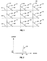
- Memory 100 includes a nXn array of memory cells 111-119, wherein memory cells 111-119 each include a select device 120 and a memory element 130.
- Memory elements 130 comprise a phase change material, thus memory 100 may be referred to as a phase change memory.
- a phase change material is a material having electrical properties (e.g. resistance, capacitance, etc.) that may be changed through the application of energy such as, for example, heat, light, voltage potential, or electrical current. Examples of a phase change material include a chalcogenide material.
- a chalcogenide alloy may be used in a memory element or in an electronic switch.
- a chalcogenide material is a material that includes at least one element from column VI of the periodic table or is a material that includes one or more of the chalcogenic elements, e.g., any of the elements of tellurium, sulfur, or selenium.
- Memory 100 includes column lines 141-143 and row lines 151-153 to select a particular memory cell of the array during a write or read operation.
- Column lines 141-143 and row lines 151-153 may also be referred to as address lines since these lines may be used to address memory cells 111-119 during programming or reading.
- Column lines 141-143 may also be referred to as bit lines and row lines 151-153 may also be referred to as word lines.
- Memory elements 130 are connected to row lines 151-153 and are coupled to column lines 141-143 via select device 120. While one select device 120 is depicted, more select devices may also be used. Therefore, when a particular memory cell (e.g., memory cell 115) is selected, voltage potentials may be applied to the memory cell's associated column line (e.g., 142) and row line (e.g., 152) to apply a voltage potential across the memory cell.
- Series connected select device 120 is used to access memory element 130 during programming or reading of memory element 130.
- the select device 120 is an ovonic threshold switch that is made of a chalcogenide alloy that does not exhibit an amorphous to crystalline phase change and which undergoes rapid, electric field initiated change in electrical conductivity that persists only so long as a holding voltage is present.
- Select device 120 operates as a switch that is either "off” or “on” depending on the amount of voltage potential applied across the memory cell, and more particularly whether the current through the select device exceeds its threshold current or voltage, which then triggers the device into the on state.
- the off state is a substantially electrically nonconductive state and the on state is a substantially conductive state, with less resistance than the off state.
- select device 120 In the on state, the voltage across the select device is equal to its holding voltage V H plus IxRon, where Ron is the dynamic resistance from V H .
- select device 120 has a threshold voltage and, if a voltage potential less than the threshold voltage of a select device 120 is applied across select device 120, then the select device 120 remains “off” or in a relatively high resistive state so that little or no electrical current passes through the memory cell and most of the voltage drop from selected row to selected column is across the select device.
- the select device 120 "turns on,” i.e., operates in a relatively low resistive state so that electrical current passes through the memory cell.
- select device 120 is in a substantially electrically nonconductive state if less than a predetermined voltage potential, e.g., the threshold voltage, is applied across select device 120.
- Select device 120 is in a substantially conductive state if greater than the predetermined voltage potential is applied across select device 120.
- Select device 120 may also be referred to as an access device, an isolation device, or a switch.
- each select device 120 comprises a switching material such as, for example, a chalcogenide alloy, and may be referred to as an ovonic threshold switch, or simply an ovonic switch.
- the switching material of select device 120 is a material in a substantially amorphous state positioned between two electrodes that may be repeatedly and reversibly switched between a higher resistance "off" state (e.g., greater than about ten megaOhms) and a relatively lower resistance "on” state (e.g., about one thousand Ohms in series with V H ) by application of a predetermined electrical current or voltage potential.
- each select device 120 is a two terminal device that has a current-voltage (I-V) characteristic similar to a phase change memory element that is in the amorphous state.
- the switching material of select device 120 does not change phase. That is, the switching material of select device 120 is not a programmable material, and, as a result, select device 120 is not a memory device capable of storing information.
- the switching material of select device 120 remains permanently amorphous and the I-V characteristic remains the same throughout the operating life.
- a representative example of I-V characteristics of select device 120 is shown in Figure 2.
- select device 120 in the low voltage or low electric field mode, i.e., where the voltage applied across select device 120 is less than a threshold voltage (labeled V TH ), select device 120 is "off" or nonconducting, and exhibits a relatively high resistance, e.g., greater than about 10 megaOhms. Select device 120 remains in the off state until a sufficient voltage, e.g., V TH , is applied, or a sufficient current is applied, e.g., I TH , that switches select device 120 to a conductive, relatively low resistance on state. After a voltage potential greater than about V TH is applied across select device 120, the voltage potential across select device 120 drops (“snapback") to a holding voltage potential, labeled V H . Snapback refers to the voltage difference between V TH and V H of a select device.
- select device 120 In the on state, the voltage potential across select device 120 remains close to the holding voltage V H as current passing through select device 120 is increased. Select device 120 remains on until the current through select device 120 drops below a holding current, labeled I H . Below this value, select device 120 turns off and returns to a relatively high resistance, nonconductive off state until the VTH and ITH are exceeded again.
- phase change memory cells there is the problem that relatively high levels of currents are required to switch the phase change material of the memory elements.
- the object of the invention is to provide a device including a phase change layer that requires less current for causing switching of the phase change layer.
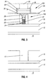
- a phase change memory cell such as a cell 111-119 in Figure 1
- a substrate 10 Over the substrate 10 various interconnections and transistor features are formed.
- An interlayer dielectric 12 separates those features from the features provided above the interlayer dielectric 12.
- a conductor 14 extends above the interlayer dielectric 12 and act as a row line 151-153 ( Figure 1).
- a conductor 36 extends generally transversely to the electrode 14 and acts as a column line 141-143 ( Figure 1).
- the dielectric layer 16 has a pore formed therein and the pore accommodates a spacer 22, a lance heater 24, and a phase change memory material 28 which, together with the heater 24, forms a phase change memory element 130 ( Figure 1).
- a region 26 of the heater 24 has a higher resistance than the region 27.
- the heater 24 is a dual resistance heater made up of the region 26 and the region 27, each region having a different resistance, although both regions may be formed of the same starting material.
- the region 27 has a lower resistance, so it creates a lower voltage drop, reducing the power consumed by the heater 24 and, thus, the cell as a whole.
- An ovonic threshold device 120 ( Figure 1) is formed above the phase change memory material 28 and acts as a selection or threshold device for the underlying memory element 130.
- the ovonic threshold device 120 is formed in a dielectric layer 18, e.g. of nitride, and in a dielectric layer 20, e.g. oxide.
- the threshold device 120 includes a lower electrode 30, an upper electrode 34, a surrounding dielectric layer 38, and a phase change memory material 32.
- the memory material 32 may, like the material 28, be a chalcogenide. However, generally, the material 32 does not change phase.
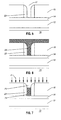
- the formation of the cell shown in Figure 3 begins with the formation of a contact or lance opening 17 in the dielectric 16, as shown in Figure 4.
- the dielectric 16 is, e.g., of oxide.
- a sidewall spacer 22 is formed in the opening 17.
- the sidewall spacer 22 may be formed by conventional techniques, including the deposition of a layer of nitride followed by anisotropic etching.
- a heater 24 is deposited to fill the opening 17.
- the heater 24 may, for example, be titanium nitride.
- the heater 24 is recessed to create the recess 25 shown in Figure 7.
- the heater 24 is planarized prior to being recessed.
- the recess 25 may be created by dry or wet etching processes known as dip backs or etch backs.
- the exposed structure is subjected to an ion implantation indicated as A in Figure 7.
- the ion implantation may be an implantation of silicon at 20keV and 10 15 atoms per square centimeter.
- a result of the implant is to convert at least an upper region 26 of the heater 24 into a higher resistance state.
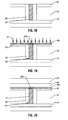
- the heater 24 is titanium nitride
- the upper region 26, shown in Figure 8 becomes titanium silicon nitride as a result of an implant followed by an effective anneal while the remaining region 27 remains titanium nitride.
- the titanium silicon nitride in the region 26 has a higher resistance than the underlying material in the region 27.
- the upper region 26 of the heater 24 has a higher resistance than the region 27.
- the upper region 26 is a very small portion of the overall heater 24.
- the heater 24 is much bigger in thickness and volume than the region 26, the region 26 only constituting a few surface layers.
- the resistance of the region 26 may be increased by an oxygen plasma treatment.
- the arrows A represent oxygen plasma which reacts with the heater 24 to form an oxide thereof. That oxide, in the region 26, has higher resistance than the underlying region 27 of the heater 24.
- a separate anneal step may not be necessary. For example, ensuing steps that involve temperature processing of 250°C may be sufficient to activate the implanted species.
- a chalcogenide material 28 is then deposited into the pore 17 with the heater 24.
- the memory material 28 acts as the phase change memory material for the cell.
- the implantation of Fig. 7 also improves adhesion of dielectric layers, such as spacer 22 and layer 16, to the material 28.
- the memory material 28 is then planarized as shown in Figure 10.
- the ovonic threshold switch 120 ( Figure 1) is then formed over the memory element 130.
- An electrode 30 is deposited, followed by the deposition of a chalcogenide material 32 that does not change phase, in turn followed by an upper electrode 34.
- the sandwich of the upper electrode 34, chalcogenide material 32, and lower electrode 30 is then patterned as indicated in Figure 12.
- the patterned structure is covered with a passivation layer 18 as shown in Figure 13.
- the passivation layer 18 may, for example, be a nitride.
- the passivation layer 18 covers the underlying portion of the dielectric 16 and the threshold device 120.
- a dielectric 20 is deposited as shown in Figure 3.
- the dielectric 20 is trenched and an upper electrode 36 is formed in the trench.
- the upper electrode may act as a column line 141-143 ( Figure 1).
- Switching material 28 is a phase change, programmable material capable of being programmed into one of at least two memory states by applying a current to switching material 28 to alter the phase of switching material 28 between a substantially crystalline state and a substantially amorphous state, wherein a resistance of switching material 28 in the substantially amorphous state is greater than the resistance of switching material 28 in the substantially crystalline state.
- Programming of switching material 28 to alter the state or phase of the material is accomplished by applying voltage potentials to the conductors 14 and 36, thereby generating a voltage potential across select device 120 and memory element 130.
- the voltage potential is greater than the threshold voltage of select device 120 and memory element 130, then an electrical current flows through memory material 28 in response to the applied voltage potential, and results in heating of memory material 28.
- This heating alters the memory state or phase of memory material 28. Altering the phase or state of memory material 28 alters the electrical characteristic of memory material 28, e.g., the resistance of the material is altered by altering the phase of the memory material 28.
- Memory material 28 is referred to as a programmable resistive material.
- memory material 28 In the "reset" state, memory material 28 is in an amorphous or semi-amorphous state and in the "set” state, memory material 28 is in a crystalline or semi-crystalline state.
- the resistance of memory material 28 in the amorphous or semi-amorphous state is greater than the resistance of memory material 28 in the crystalline or semi-crystalline state.
- memory material 28 is heated to a relatively higher temperature to amorphosize memory material 28 and "reset” memory material 28 (e.g., program memory material 28 to a logic "0" value). Heating the volume of memory material 28 to a relatively lower crystallization temperature crystallizes memory material 28 and "sets" memory material 28 (e.g., program memory material 28 to a logic "1" value).
- Various resistances of memory material 28 may be achieved to store information by varying the amount of current flow and duration through the volume of memory material 28.
- the composition of switching material 32 may comprise a Si concentration of about 14%, a Te concentration of about 39%, an As concentration of about 37%, a Ge concentration of about 9%, and an In concentration of about 1%.
- the composition of switching material 32 may comprise a Si concentration of about 14%, a Te concentration of about 39%, an As concentration of about 37%, a Ge concentration of about 9%, and a P concentration of about 1%.
- the percentages are atomic percentages which total 100% of the atoms of the constituent elements.
- a composition for switching material 32 includes an alloy of arsenic (As), tellurium (Te), sulfur (S), germanium (Ge), selenium (Se), and antimony (Sb) with respective atomic percentages of 10%, 21%, 2%, 15%, 50%, and 2%.
- switching material 32 includes Si, Te, As, Ge, sulfur (S), and selenium (Se).
- the composition of switching material 32 comprises a Si concentration of about 5%, a Te concentration of about 34%, an As concentration of about 28%, a Ge concentration of about 11%, a S concentration of about 21%, and a Se concentration of about 1%.
- the switching material 32 is a thin film material having a thickness ranging from about 20 ⁇ to about 2000 ⁇ . In one embodiment, the thickness of the material 32 ranges from about 100 ⁇ to about 1000 ⁇ . In another embodiment, the thickness of the material 32 is about 300 ⁇ .
- Suitable materials for electrodes 30 and 34 include a thin film of titanium (Ti), titanium nitride (TiN), titanium tungsten (TiW), carbon (C), silicon carbide (SiC), titanium aluminum nitride (TiAlN), titanium silicon nitride (TiSiN), polycrystalline silicon, tantalum nitride (TaN), some combination of these films, or other suitable conductors or resistive conductors compatible with switching material 32.
- System 500 may be used in wireless devices such as, for example, a personal digital assistant (PDA), a laptop or portable computer with wireless capability, a web tablet, a wireless telephone, a pager, an instant messaging device, a digital music player, a digital camera, or other devices that may be adapted to transmit and/or receive information wirelessly.
- PDA personal digital assistant
- System 500 may be used in any of the following systems: a wireless local area network (WLAN) system, a wireless personal area network (WPAN) system, a cellular network, although the scope of the present invention is not limited in this respect.
- WLAN wireless local area network
- WPAN wireless personal area network
- cellular network although the scope of the present invention is not limited in this respect.
- System 500 includes a controller 510, an input/output (I/O) device 520 (e.g. a keypad, display), a memory 530, and a wireless interface 540 coupled to each other via a bus 550.
- I/O input/output
- Controller 510 may comprise, for example, one or more microprocessors, digital signal processors, microcontrollers, or the like.
- Memory 530 may be used to store messages transmitted to or by system 500. Memory 530 may also optionally be used to store instructions that are executed by controller 510 during the operation of system 500, and may be used to store user data.
- Memory 530 may be provided by one or more different types of memory. For example, memory 530 may comprise any type of random access memory, a volatile memory, a non-volatile memory such as a flash memory and/or a memory 100 discussed herein.
- I/O device 520 may be used by a user to generate a message.
- System 500 may use wireless interface 540 to transmit and receive messages to and from a wireless communication network with a radio frequency (RF) signal.
- Examples of wireless interface 540 may include an antenna or a wireless transceiver.
- the dielectric region surrounding the heater is treated to improve the adhesion properties thereof.
- a second dielectric layer 40 is formed over the dielectric layer 16 and the stack of the dielectric layer 16 and the second dielectric layer 40 is etched to form an opening 42 defining a contact opening structure.
- the remaining structure of Figure 15 is similar to the structure previously described in connection with Figure 4.
- the opening 42 is covered with a sidewall spacer 45, using known techniques.
- the spacer 45 is e.g. of nitride.
- the heater 24 is deposited to completely fill the remaining opening 42 and to cover the top of the second dielectric layer 40.
- This structure is then planarized in a timed polish so as to remove a portion of the second dielectric layer 40, and to polish away the flared region 41 of the spacer 45, as shown in Figure 18.
- a silicon implant is accomplished as indicated at B in Figure 19.
- the implant converts the top portion 40a of the second dielectric layer 40 to silicon nitride.
- the implant conditions are the same as those described previously in connection with Figure 7.
- Silicon-implanted nitride has good adhesion to overlying layers including chalcogenide containing layers.
- the silicon-implanted nitride layer 40a acts as a glue or adhesion layer.
- the implanted region 24b of the heater 24 is converted to titanium silicon nitride, which has higher resistivity than the non-implanted titanium nitride region 27.
- Annealed silicon-implanted titanium nitride, or titanium silicon nitride has a very high adhesion to overlying layers including chalcogenide containing layers.
- a dual resistance heater 24 is formed at the same time that the top portion 40a of the second dielectric layer 40 is modified to make it an effective glue layer.
- the top portion 40a of the second dielectric layer 40 is substantially planar. In other words, it does not extend into the opening 42 that includes the heater 24.
- a chalcogenide layer 46 is deposited, followed by an upper electrode 48. Then, referring to Figure 21, the upper electrode 48 and the chalcogenide layer 46 are patterned.
Landscapes
- Engineering & Computer Science (AREA)
- Manufacturing & Machinery (AREA)
- Semiconductor Memories (AREA)
Priority Applications (6)
| Application Number | Priority Date | Filing Date | Title |
|---|---|---|---|
| EP04107070A EP1677371A1 (de) | 2004-12-30 | 2004-12-30 | Zweiteiliger Widerstandsheizer für Phasenwechselspeicher und Herstellungsmethode |
| US11/312,231 US7880123B2 (en) | 2004-12-30 | 2005-12-19 | Dual resistance heater for phase change devices and manufacturing method thereof |
| US12/980,141 US8513576B2 (en) | 2004-12-30 | 2010-12-28 | Dual resistance heater for phase change devices and manufacturing method thereof |
| US13/970,207 US8952299B2 (en) | 2004-12-30 | 2013-08-19 | Dual resistance heater for phase change devices and manufacturing method thereof |
| US14/615,963 US10522756B2 (en) | 2004-12-30 | 2015-02-06 | Dual resistance heater for phase change memory devices |
| US15/851,081 US10522757B2 (en) | 2004-12-30 | 2017-12-21 | Dual resistive-material regions for phase change memory devices |
Applications Claiming Priority (1)
| Application Number | Priority Date | Filing Date | Title |
|---|---|---|---|
| EP04107070A EP1677371A1 (de) | 2004-12-30 | 2004-12-30 | Zweiteiliger Widerstandsheizer für Phasenwechselspeicher und Herstellungsmethode |
Publications (1)
| Publication Number | Publication Date |
|---|---|
| EP1677371A1 true EP1677371A1 (de) | 2006-07-05 |
Family
ID=34930198
Family Applications (1)
| Application Number | Title | Priority Date | Filing Date |
|---|---|---|---|
| EP04107070A Withdrawn EP1677371A1 (de) | 2004-12-30 | 2004-12-30 | Zweiteiliger Widerstandsheizer für Phasenwechselspeicher und Herstellungsmethode |
Country Status (2)
| Country | Link |
|---|---|
| US (5) | US7880123B2 (de) |
| EP (1) | EP1677371A1 (de) |
Families Citing this family (61)
| Publication number | Priority date | Publication date | Assignee | Title |
|---|---|---|---|---|
| EP1677371A1 (de) | 2004-12-30 | 2006-07-05 | STMicroelectronics S.r.l. | Zweiteiliger Widerstandsheizer für Phasenwechselspeicher und Herstellungsmethode |
| US7910904B2 (en) * | 2005-05-12 | 2011-03-22 | Ovonyx, Inc. | Multi-level phase change memory |
| US8188454B2 (en) * | 2005-10-28 | 2012-05-29 | Ovonyx, Inc. | Forming a phase change memory with an ovonic threshold switch |
| TWI346382B (en) * | 2007-03-30 | 2011-08-01 | Nanya Technology Corp | Phase change memory devices and fabrication methods thereof |
| US9203024B2 (en) * | 2007-07-25 | 2015-12-01 | Intel Corporation | Copper compatible chalcogenide phase change memory with adjustable threshold voltage |
| US8189372B2 (en) * | 2008-02-05 | 2012-05-29 | International Business Machines Corporation | Integrated circuit including electrode having recessed portion |
| US7990761B2 (en) * | 2008-03-31 | 2011-08-02 | Ovonyx, Inc. | Immunity of phase change material to disturb in the amorphous phase |
| KR101019986B1 (ko) * | 2008-10-10 | 2011-03-09 | 주식회사 하이닉스반도체 | 성장 방식에 의해 형성되는 콘택 구조를 절연시키는 절연막을 포함하는 상변화 메모리 소자, 이를 포함하는 반도체 소자, 및 그들의 제조방법 |
| US8138056B2 (en) | 2009-07-03 | 2012-03-20 | International Business Machines Corporation | Thermally insulated phase change material memory cells with pillar structure |
| US8530875B1 (en) * | 2010-05-06 | 2013-09-10 | Micron Technology, Inc. | Phase change memory including ovonic threshold switch with layered electrode and methods for forming same |
| US8247789B2 (en) * | 2010-08-31 | 2012-08-21 | Micron Technology, Inc. | Memory cells and methods of forming memory cells |
| KR101908062B1 (ko) | 2012-03-29 | 2018-10-15 | 삼성전자주식회사 | 상변화 메모리 장치 및 이의 제조 방법 |
| CN104470387B (zh) | 2012-12-28 | 2016-06-01 | 菲利普莫里斯生产公司 | 气溶胶产生系统的加热组件 |
| US9166158B2 (en) | 2013-02-25 | 2015-10-20 | Micron Technology, Inc. | Apparatuses including electrodes having a conductive barrier material and methods of forming same |
| US9419213B2 (en) * | 2014-06-06 | 2016-08-16 | The Regents Of The University Of Michigan | Directly heated RF phase change switch |
| CN105244437A (zh) * | 2014-07-08 | 2016-01-13 | 中芯国际集成电路制造(上海)有限公司 | 相变存储器及其形成方法 |
| US9362492B2 (en) | 2014-08-25 | 2016-06-07 | Qualcomm Switch Corp. | Integrated phase change switch |
| KR102375591B1 (ko) | 2015-10-27 | 2022-03-16 | 삼성전자주식회사 | 반도체 장치 및 이의 제조 방법 |
| KR102295524B1 (ko) | 2017-03-27 | 2021-08-30 | 삼성전자 주식회사 | 메모리 소자 |
| US11031072B2 (en) * | 2017-09-28 | 2021-06-08 | Intel Corporation | Dynamic random access memory including threshold switch |
| US11152569B2 (en) * | 2017-11-30 | 2021-10-19 | Taiwan Semiconductor Manufacturing Co., Ltd. | PCRAM structure with selector device |
| KR102665246B1 (ko) | 2018-07-03 | 2024-05-09 | 삼성전자주식회사 | 반도체 장치 및 이의 제조 방법 |
| US10739290B2 (en) | 2018-08-14 | 2020-08-11 | Newport Fab, Llc | Read out integrated circuit (ROIC) for rapid testing and characterization of conductivity skew of phase-change material (PCM) in PCM radio frequency (RF) switches |
| US11057019B2 (en) | 2018-08-14 | 2021-07-06 | Newport Fab, Llc | Non-volatile adjustable phase shifter using non-volatile radio frequency (RF) switch |
| US10686128B2 (en) | 2018-08-14 | 2020-06-16 | Newport Fab, Llc | Semiconductor devices having phase-change material (PCM) radio frequency (RF) switches and integrated passive devices |
| US10454027B1 (en) | 2018-08-14 | 2019-10-22 | Newport Fab, Llc | Phase-change material (PCM) radio frequency (RF) switches with stressor layers and contact adhesion layers |
| US10461253B1 (en) | 2018-08-14 | 2019-10-29 | Newport Fab, Llc | High reliability RF switch based on phase-change material |
| US10686010B2 (en) | 2018-08-14 | 2020-06-16 | Newport Fab, Llc | Fabrication of semiconductor device using a shared material in a phase-change material (PCM) switch region and a resonator region |
| US10644236B2 (en) | 2018-08-14 | 2020-05-05 | Newport Fab, Llc | Phase-change material (PCM) radio frequency (RF) switch with reduced parasitic capacitance |
| US10833004B2 (en) | 2018-08-14 | 2020-11-10 | Newport Fab, Llc Dba Jazz Semiconductor | Capacitive tuning circuit using RF switches with PCM capacitors and PCM contact capacitors |
| US10862477B2 (en) | 2018-08-14 | 2020-12-08 | Newport Fab, Llc | Read out integrated circuit (ROIC) for rapid testing of functionality of phase-change material (PCM) radio frequency (RF) switches |
| US10615338B2 (en) | 2018-08-14 | 2020-04-07 | Newport Fab, Llc | Phase-change material (PCM) contacts with slot lower portions and contact dielectric for reducing parasitic capacitance and improving manufacturability in PCM RF switches |
| US10862032B2 (en) | 2018-08-14 | 2020-12-08 | Newport Fab, Llc | Phase-change material (PCM) radio frequency (RF) switch |
| US10978639B2 (en) | 2018-08-14 | 2021-04-13 | Newport Fab, Llc | Circuits for reducing RF signal interference and for reducing DC power loss in phase-change material (PCM) RF switches |
| US10593404B2 (en) | 2018-08-14 | 2020-03-17 | Newport Fab, Llc | Array architecture for large scale integration of phase-change material (PCM) radio frequency (RF) switches |
| US10686130B2 (en) | 2018-08-14 | 2020-06-16 | Newport Fab, Llc | Phase-change material (PCM) contact configurations for improving performance in PCM RF switches |
| US10944052B2 (en) | 2018-08-14 | 2021-03-09 | Newport Fab, Llc | Phase-change material (PCM) radio frequency (RF) switch using a chemically protective and thermally conductive layer |
| US10622560B2 (en) * | 2018-08-14 | 2020-04-14 | Newport Fab, Llc | Semiconductor chips and systems having phase-change material (PCM) switches integrated with micro-electrical-mechanical systems (MEMS) and/or resonators |
| US10770389B2 (en) | 2018-08-14 | 2020-09-08 | Newport Fab, Llc | Phase-change material (PCM) radio frequency (RF) switches with capacitively coupled RF terminals |
| US11050022B2 (en) | 2018-08-14 | 2021-06-29 | Newport Fab, Llc | Radio frequency (RF) switches having phase-change material (PCM) and heat management for increased manufacturability and performance |
| US11159145B2 (en) | 2018-08-14 | 2021-10-26 | Newport Fab, Llc | Radio frequency (RF) filtering using phase-change material (PCM) RF switches |
| US10566528B1 (en) | 2018-08-14 | 2020-02-18 | Newport Fab, Llc | Heating element designs for phase-change material (PCM) radio frequency (RF) switches |
| US11196401B2 (en) | 2018-08-14 | 2021-12-07 | Newport Fab, Llc | Radio frequency (RF) module using a tunable RF filter with non-volatile RF switches |
| US10916585B2 (en) | 2018-08-14 | 2021-02-09 | Newport Fab, Llc | Stacked phase-change material (PCM) radio frequency (RF) switches with improved RF power handling |
| US10475993B1 (en) | 2018-08-14 | 2019-11-12 | Newport Fab, Llc | PCM RF switch fabrication with subtractively formed heater |
| US10937960B2 (en) | 2018-08-14 | 2021-03-02 | Newport Fab, Llc | Concurrent fabrication of and structure for capacitive terminals and ohmic terminals in a phase-change material (PCM) radio frequency (RF) switch |
| US10707125B2 (en) | 2018-08-14 | 2020-07-07 | Newport Fab, Llc | Fabrication of contacts in an RF switch having a phase-change material (PCM) and a heating element |
| US10644235B2 (en) * | 2018-08-14 | 2020-05-05 | Newport Fab, Llc | Phase-change material (PCM) radio frequency (RF) switch with reduced parasitic capacitance |
| US10749109B2 (en) | 2018-08-14 | 2020-08-18 | Newport Fab, Llc | Read out integrated circuit (ROIC) for rapid testing and characterization of resistivity change of heating element in phase-change material (PCM) radio frequency (RF) switch |
| US10566321B1 (en) | 2018-08-14 | 2020-02-18 | Newport Fab, Llc | Wafer-to-wafer and die-to-wafer bonding of phase-change material (PCM) switches with integrated circuits and bonded two-die devices |
| US10770657B2 (en) | 2018-08-14 | 2020-09-08 | Newport Fab, Llc | High reliability phase-change material (PCM) radio frequency (RF) switch using trap-rich region |
| US10693061B2 (en) | 2018-08-14 | 2020-06-23 | Newport Fab, Llc | Semiconductor devices having phase-change material (PCM) radio frequency (RF) switches and integrated active devices |
| US10476001B1 (en) * | 2018-08-14 | 2019-11-12 | Newport Fab, Llc | Manufacturing RF switch based on phase-change material |
| US10529922B1 (en) | 2018-08-14 | 2020-01-07 | Newport Fab, Llc | Substrates and heat spreaders for heat management and RF isolation in integrated semiconductor devices having phase-change material (PCM) radio frequency (RF) switches |
| US10916540B2 (en) | 2018-08-14 | 2021-02-09 | Newport Fab, Llc | Device including PCM RF switch integrated with group III-V semiconductors |
| US11139430B2 (en) | 2018-10-31 | 2021-10-05 | Taiwan Semiconductor Manufacturing Co., Ltd. | Phase change random access memory and method of manufacturing |
| KR102614852B1 (ko) | 2018-11-14 | 2023-12-19 | 삼성전자주식회사 | 메모리 장치, 메모리 셀 및 메모리 셀 프로그래밍 방법 |
| US11659780B2 (en) * | 2019-03-05 | 2023-05-23 | International Business Machines Corporation | Phase change memory structure with efficient heating system |
| FR3096826B1 (fr) * | 2019-05-28 | 2022-06-03 | St Microelectronics Srl | Cellule mémoire |
| KR20200140601A (ko) | 2019-06-07 | 2020-12-16 | 삼성전자주식회사 | 정보 저장 물질 패턴을 포함하는 반도체 소자 |
| FR3107138B1 (fr) | 2020-02-06 | 2022-02-11 | Commissariat Energie Atomique | Cellule mémoire à changement de phase |
Citations (5)
| Publication number | Priority date | Publication date | Assignee | Title |
|---|---|---|---|---|
| WO2002009206A1 (en) * | 2000-07-22 | 2002-01-31 | Ovonyx, Inc. | Electrically programmable memory element |
| KR100364805B1 (ko) * | 2000-12-28 | 2002-12-16 | 주식회사 하이닉스반도체 | 반도체 소자의 금속배선 형성방법 |
| EP1331675A1 (de) * | 2002-01-17 | 2003-07-30 | STMicroelectronics S.r.l. | Integriertes Widerstandselement, Phasenwechsel Speicherelement mit solchem Widerstandselement, und Verfahren zu seiner Herstellung |
| US20040067608A1 (en) * | 2000-12-14 | 2004-04-08 | Charles Dennison | Method to selectively increase the top resistance of the lower programming electrode in a phase-change memory cell and structures obtained thereby |
| KR100448854B1 (ko) * | 2001-12-29 | 2004-09-18 | 주식회사 하이닉스반도체 | 반도체소자의 캐패시터 형성방법 |
Family Cites Families (83)
| Publication number | Priority date | Publication date | Assignee | Title |
|---|---|---|---|---|
| US3271591A (en) * | 1963-09-20 | 1966-09-06 | Energy Conversion Devices Inc | Symmetrical current controlling device |
| US4003075A (en) * | 1971-03-09 | 1977-01-11 | Innotech Corporation | Glass electronic devices employing ion-doped insulating glassy amorphous material |
| US3886577A (en) * | 1973-09-12 | 1975-05-27 | Energy Conversion Devices Inc | Filament-type memory semiconductor device and method of making the same |
| US3922648A (en) * | 1974-08-19 | 1975-11-25 | Energy Conversion Devices Inc | Method and means for preventing degradation of threshold voltage of filament-forming memory semiconductor device |
| US4177475A (en) * | 1977-10-31 | 1979-12-04 | Burroughs Corporation | High temperature amorphous memory device for an electrically alterable read-only memory |
| US4225946A (en) * | 1979-01-24 | 1980-09-30 | Harris Corporation | Multilevel erase pulse for amorphous memory devices |
| US4499557A (en) * | 1980-10-28 | 1985-02-12 | Energy Conversion Devices, Inc. | Programmable cell for use in programmable electronic arrays |
| JPS5893221A (ja) * | 1981-11-30 | 1983-06-02 | Toshiba Corp | 半導体薄膜構造とその製造方法 |
| US4782340A (en) * | 1986-08-22 | 1988-11-01 | Energy Conversion Devices, Inc. | Electronic arrays having thin film line drivers |
| US5210766A (en) * | 1990-12-27 | 1993-05-11 | Xerox Corporation | Laser crystallized cladding layers for improved amorphous silicon light-emitting diodes and radiation sensors |
| US5330630A (en) * | 1991-01-02 | 1994-07-19 | Energy Conversion Devices, Inc. | Switch with improved threshold voltage |
| US5596522A (en) * | 1991-01-18 | 1997-01-21 | Energy Conversion Devices, Inc. | Homogeneous compositions of microcrystalline semiconductor material, semiconductor devices and directly overwritable memory elements fabricated therefrom, and arrays fabricated from the memory elements |
| US5208172A (en) * | 1992-03-02 | 1993-05-04 | Motorola, Inc. | Method for forming a raised vertical transistor |
| US5439840A (en) * | 1993-08-02 | 1995-08-08 | Motorola, Inc. | Method of forming a nonvolatile random access memory capacitor cell having a metal-oxide dielectric |
| US5363329A (en) * | 1993-11-10 | 1994-11-08 | Eugeniy Troyan | Semiconductor memory device for use in an electrically alterable read-only memory |
| US6420725B1 (en) * | 1995-06-07 | 2002-07-16 | Micron Technology, Inc. | Method and apparatus for forming an integrated circuit electrode having a reduced contact area |
| JPH0964209A (ja) * | 1995-08-25 | 1997-03-07 | Toshiba Corp | 半導体装置およびその製造方法 |
| US5726484A (en) * | 1996-03-06 | 1998-03-10 | Xilinx, Inc. | Multilayer amorphous silicon antifuse |
| US6025220A (en) * | 1996-06-18 | 2000-02-15 | Micron Technology, Inc. | Method of forming a polysilicon diode and devices incorporating such diode |
| US5789277A (en) * | 1996-07-22 | 1998-08-04 | Micron Technology, Inc. | Method of making chalogenide memory device |
| US6147395A (en) * | 1996-10-02 | 2000-11-14 | Micron Technology, Inc. | Method for fabricating a small area of contact between electrodes |
| US5825046A (en) * | 1996-10-28 | 1998-10-20 | Energy Conversion Devices, Inc. | Composite memory material comprising a mixture of phase-change memory material and dielectric material |
| US6617192B1 (en) * | 1997-10-01 | 2003-09-09 | Ovonyx, Inc. | Electrically programmable memory element with multi-regioned contact |
| US5937297A (en) * | 1998-06-01 | 1999-08-10 | Chartered Semiconductor Manufacturing, Ltd. | Method for making sub-quarter-micron MOSFET |
| US6936892B2 (en) * | 1998-07-24 | 2005-08-30 | Fuji Electric Co., Ltd. | Semiconductor device with alternating conductivity type layer and method of manufacturing the same |
| CA2367365A1 (en) * | 1999-03-25 | 2000-09-28 | Stanford R. Ovshinsky | Electrically programmable memory element with improved contacts |
| US7074640B2 (en) * | 2000-06-06 | 2006-07-11 | Simon Fraser University | Method of making barrier layers |
| US6339544B1 (en) * | 2000-09-29 | 2002-01-15 | Intel Corporation | Method to enhance performance of thermal resistor device |
| US6555860B2 (en) * | 2000-09-29 | 2003-04-29 | Intel Corporation | Compositionally modified resistive electrode |
| DE10055215A1 (de) * | 2000-11-07 | 2002-05-08 | Walter Hillebrand Galvanotechn | Passivierungsverfahren |
| US6646297B2 (en) * | 2000-12-26 | 2003-11-11 | Ovonyx, Inc. | Lower electrode isolation in a double-wide trench |
| US6709945B2 (en) * | 2001-01-16 | 2004-03-23 | Micron Technology, Inc. | Reduced aspect ratio digit line contact process flow used during the formation of a semiconductor device |
| KR100385951B1 (ko) * | 2001-01-17 | 2003-06-02 | 삼성전자주식회사 | 다중층의 스토리지 노드 콘택 플러그를 갖는 반도체메모리 소자 및 그 제조방법 |
| US6613604B2 (en) * | 2001-08-02 | 2003-09-02 | Ovonyx, Inc. | Method for making small pore for use in programmable resistance memory element |
| US6511862B2 (en) * | 2001-06-30 | 2003-01-28 | Ovonyx, Inc. | Modified contact for programmable devices |
| US6507061B1 (en) * | 2001-08-31 | 2003-01-14 | Intel Corporation | Multiple layer phase-change memory |
| US6586761B2 (en) * | 2001-09-07 | 2003-07-01 | Intel Corporation | Phase change material memory device |
| US6566700B2 (en) * | 2001-10-11 | 2003-05-20 | Ovonyx, Inc. | Carbon-containing interfacial layer for phase-change memory |
| EP1318552A1 (de) | 2001-12-05 | 2003-06-11 | STMicroelectronics S.r.l. | Kleinflächige Kontaktzone, hocheffizientes Phasenwechsel-Speicherelement und dessen Verfahren zur Herstellung |
| US6545903B1 (en) | 2001-12-17 | 2003-04-08 | Texas Instruments Incorporated | Self-aligned resistive plugs for forming memory cell with phase change material |
| US6891747B2 (en) * | 2002-02-20 | 2005-05-10 | Stmicroelectronics S.R.L. | Phase change memory cell and manufacturing method thereof using minitrenches |
| US6930913B2 (en) * | 2002-02-20 | 2005-08-16 | Stmicroelectronics S.R.L. | Contact structure, phase change memory cell, and manufacturing method thereof with elimination of double contacts |
| JP4103497B2 (ja) * | 2002-04-18 | 2008-06-18 | ソニー株式会社 | 記憶装置とその製造方法および使用方法、半導体装置とその製造方法 |
| US6844582B2 (en) * | 2002-05-10 | 2005-01-18 | Matsushita Electric Industrial Co., Ltd. | Semiconductor device and learning method thereof |
| KR100448893B1 (ko) * | 2002-08-23 | 2004-09-16 | 삼성전자주식회사 | 상전이 기억 소자 구조 및 그 제조 방법 |
| JP4190238B2 (ja) * | 2002-09-13 | 2008-12-03 | 株式会社ルネサステクノロジ | 不揮発性半導体記憶装置 |
| US7314776B2 (en) * | 2002-12-13 | 2008-01-01 | Ovonyx, Inc. | Method to manufacture a phase change memory |
| US6795338B2 (en) * | 2002-12-13 | 2004-09-21 | Intel Corporation | Memory having access devices using phase change material such as chalcogenide |
| US6791102B2 (en) * | 2002-12-13 | 2004-09-14 | Intel Corporation | Phase change memory |
| US6869883B2 (en) * | 2002-12-13 | 2005-03-22 | Ovonyx, Inc. | Forming phase change memories |
| US7242019B2 (en) * | 2002-12-13 | 2007-07-10 | Intel Corporation | Shunted phase change memory |
| DE60331629D1 (de) * | 2003-01-15 | 2010-04-22 | St Microelectronics Srl | Verfahren zur Herstellung einer Speichervorrichtung, insbesondere eines Phasenwechselspeichers, mit einem Silizidierungsschritt |
| JP4254293B2 (ja) * | 2003-03-25 | 2009-04-15 | 株式会社日立製作所 | 記憶装置 |
| US7129560B2 (en) * | 2003-03-31 | 2006-10-31 | International Business Machines Corporation | Thermal memory cell and memory device including the thermal memory cell |
| DE60306893T2 (de) * | 2003-05-07 | 2007-02-01 | Stmicroelectronics S.R.L., Agrate Brianza | Verfahren zur Herstellung einer elektrischen Speichereinrichtung mit Auswahltransistoren für Speicherelemente sowie entsprechend hergestellte Speichereinrichtung |
| JP4634014B2 (ja) | 2003-05-22 | 2011-02-16 | 株式会社日立製作所 | 半導体記憶装置 |
| EP1482551B1 (de) * | 2003-05-26 | 2007-02-07 | STMicroelectronics S.r.l. | Herstellung dünner Schichten aus TiSiN, besonders für Phasenwechselspeicher |
| US6858883B2 (en) | 2003-06-03 | 2005-02-22 | Hewlett-Packard Development Company, L.P. | Partially processed tunnel junction control element |
| KR100504701B1 (ko) * | 2003-06-11 | 2005-08-02 | 삼성전자주식회사 | 상변화 기억 소자 및 그 형성 방법 |
| US20050032269A1 (en) * | 2003-08-04 | 2005-02-10 | Daniel Xu | Forming planarized semiconductor structures |
| US7161167B2 (en) * | 2003-08-04 | 2007-01-09 | Intel Corporation | Lateral phase change memory |
| US20050029504A1 (en) * | 2003-08-04 | 2005-02-10 | Karpov Ilya V. | Reducing parasitic conductive paths in phase change memories |
| US6815704B1 (en) * | 2003-09-04 | 2004-11-09 | Silicon Storage Technology, Inc. | Phase change memory device employing thermally insulating voids |
| US7074707B2 (en) | 2003-09-15 | 2006-07-11 | International Business Machines Corporation | Method of fabricating a connection device |
| JP4308625B2 (ja) * | 2003-11-07 | 2009-08-05 | パナソニック株式会社 | メモリ混載半導体装置及びその製造方法 |
| JP4567963B2 (ja) * | 2003-12-05 | 2010-10-27 | ルネサスエレクトロニクス株式会社 | 半導体集積回路装置 |
| US7038231B2 (en) * | 2004-04-30 | 2006-05-02 | International Business Machines Corporation | Non-planarized, self-aligned, non-volatile phase-change memory array and method of formation |
| DE102004024647B4 (de) * | 2004-05-18 | 2006-03-16 | Siemens Ag | Verfahren und Funkstation zur Regulierung von Zugriffsraten in einem Funkkommunikationssystem |
| US7348268B2 (en) * | 2004-09-10 | 2008-03-25 | Intel Corporation | Controlled breakdown phase change memory device |
| US7227239B2 (en) * | 2004-09-23 | 2007-06-05 | International Business Machines Corporation | Resettable fuse device and method of fabricating the same |
| US7023008B1 (en) * | 2004-09-30 | 2006-04-04 | Infineon Technologies Ag | Resistive memory element |
| US8501523B2 (en) | 2004-10-28 | 2013-08-06 | Micron Technology, Inc. | Depositing titanium silicon nitride films for forming phase change memories |
| KR100827653B1 (ko) * | 2004-12-06 | 2008-05-07 | 삼성전자주식회사 | 상변화 기억 셀들 및 그 제조방법들 |
| EP1677371A1 (de) * | 2004-12-30 | 2006-07-05 | STMicroelectronics S.r.l. | Zweiteiliger Widerstandsheizer für Phasenwechselspeicher und Herstellungsmethode |
| JP4890016B2 (ja) * | 2005-03-16 | 2012-03-07 | ルネサスエレクトロニクス株式会社 | 不揮発性半導体記憶装置 |
| JP2008053494A (ja) * | 2006-08-25 | 2008-03-06 | Elpida Memory Inc | 半導体装置及びその製造方法 |
| US7511984B2 (en) * | 2006-08-30 | 2009-03-31 | Micron Technology, Inc. | Phase change memory |
| US7593254B2 (en) * | 2007-05-25 | 2009-09-22 | Micron Technology, Inc. | Variable resistance memory device with an interfacial adhesion heating layer, systems using the same and methods of forming the same |
| US7838341B2 (en) * | 2008-03-14 | 2010-11-23 | Ovonyx, Inc. | Self-aligned memory cells and method for forming |
| JP5127630B2 (ja) * | 2008-08-20 | 2013-01-23 | 株式会社東芝 | 抵抗変化型メモリ |
| JP4846817B2 (ja) * | 2009-03-23 | 2011-12-28 | 株式会社東芝 | 抵抗変化型メモリ |
| US8530875B1 (en) * | 2010-05-06 | 2013-09-10 | Micron Technology, Inc. | Phase change memory including ovonic threshold switch with layered electrode and methods for forming same |
| US8283198B2 (en) * | 2010-05-10 | 2012-10-09 | Micron Technology, Inc. | Resistive memory and methods of processing resistive memory |
-
2004
- 2004-12-30 EP EP04107070A patent/EP1677371A1/de not_active Withdrawn
-
2005
- 2005-12-19 US US11/312,231 patent/US7880123B2/en active Active
-
2010
- 2010-12-28 US US12/980,141 patent/US8513576B2/en active Active
-
2013
- 2013-08-19 US US13/970,207 patent/US8952299B2/en active Active
-
2015
- 2015-02-06 US US14/615,963 patent/US10522756B2/en active Active
-
2017
- 2017-12-21 US US15/851,081 patent/US10522757B2/en active Active
Patent Citations (5)
| Publication number | Priority date | Publication date | Assignee | Title |
|---|---|---|---|---|
| WO2002009206A1 (en) * | 2000-07-22 | 2002-01-31 | Ovonyx, Inc. | Electrically programmable memory element |
| US20040067608A1 (en) * | 2000-12-14 | 2004-04-08 | Charles Dennison | Method to selectively increase the top resistance of the lower programming electrode in a phase-change memory cell and structures obtained thereby |
| KR100364805B1 (ko) * | 2000-12-28 | 2002-12-16 | 주식회사 하이닉스반도체 | 반도체 소자의 금속배선 형성방법 |
| KR100448854B1 (ko) * | 2001-12-29 | 2004-09-18 | 주식회사 하이닉스반도체 | 반도체소자의 캐패시터 형성방법 |
| EP1331675A1 (de) * | 2002-01-17 | 2003-07-30 | STMicroelectronics S.r.l. | Integriertes Widerstandselement, Phasenwechsel Speicherelement mit solchem Widerstandselement, und Verfahren zu seiner Herstellung |
Non-Patent Citations (2)
| Title |
|---|
| DATABASE WPI Section Ch Week 200336, Derwent World Patents Index; Class L03, AN 2003-054657, XP002323292 * |
| DATABASE WPI Section Ch Week 200508, Derwent World Patents Index; Class L03, AN 2003-892827, XP002323291 * |
Also Published As
| Publication number | Publication date |
|---|---|
| US8513576B2 (en) | 2013-08-20 |
| US10522756B2 (en) | 2019-12-31 |
| US20140038379A1 (en) | 2014-02-06 |
| US7880123B2 (en) | 2011-02-01 |
| US20060246712A1 (en) | 2006-11-02 |
| US20110155986A1 (en) | 2011-06-30 |
| US20150188050A1 (en) | 2015-07-02 |
| US10522757B2 (en) | 2019-12-31 |
| US20180138406A1 (en) | 2018-05-17 |
| US8952299B2 (en) | 2015-02-10 |
Similar Documents
| Publication | Publication Date | Title |
|---|---|---|
| US10522757B2 (en) | Dual resistive-material regions for phase change memory devices | |
| US7709822B2 (en) | Phase change memory and manufacturing method thereof | |
| EP1771861B1 (de) | Zugriff auf phasenänderungsspeicher | |
| US9747975B2 (en) | Multi-level phase change memory | |
| US7135696B2 (en) | Phase change memory with damascene memory element | |
| US7282730B2 (en) | Forming a carbon layer between phase change layers of a phase change memory | |
| US8187946B2 (en) | Manufacturing a phase change memory device having a ring heater | |
| US20060278900A1 (en) | Phase change memory device having an adhesion layer and manufacturing process thereof | |
| US7655938B2 (en) | Phase change memory with U-shaped chalcogenide cell | |
| US7105408B2 (en) | Phase change memory with a select device having a breakdown layer | |
| US20060255328A1 (en) | Using conductive oxidation for phase change memory electrodes | |
| US20060226410A1 (en) | Heating phase change material |
Legal Events
| Date | Code | Title | Description |
|---|---|---|---|
| PUAI | Public reference made under article 153(3) epc to a published international application that has entered the european phase |
Free format text: ORIGINAL CODE: 0009012 |
|
| AK | Designated contracting states |
Kind code of ref document: A1 Designated state(s): AT BE BG CH CY CZ DE DK EE ES FI FR GB GR HU IE IS IT LI LT LU MC NL PL PT RO SE SI SK TR |
|
| AX | Request for extension of the european patent |
Extension state: AL BA HR LV MK YU |
|
| RIN1 | Information on inventor provided before grant (corrected) |
Inventor name: LOWREY, TYLER Inventor name: MARANGON, MARIA SANTINA Inventor name: ATWOOD, GREG Inventor name: KUO, CHARLES C. Inventor name: KARPOV, ILYA V. Inventor name: KIM, YUDONG |
|
| AKX | Designation fees paid | ||
| REG | Reference to a national code |
Ref country code: DE Ref legal event code: 8566 |
|
| STAA | Information on the status of an ep patent application or granted ep patent |
Free format text: STATUS: THE APPLICATION IS DEEMED TO BE WITHDRAWN |
|
| 18D | Application deemed to be withdrawn |
Effective date: 20070105 |