EP1676096B1 - X-y axis dual-mass tuning fork gyroscope with vertically integrated electronics and wafer-scale hermetic packaging - Google Patents
X-y axis dual-mass tuning fork gyroscope with vertically integrated electronics and wafer-scale hermetic packaging Download PDFInfo
- Publication number
- EP1676096B1 EP1676096B1 EP04795573.7A EP04795573A EP1676096B1 EP 1676096 B1 EP1676096 B1 EP 1676096B1 EP 04795573 A EP04795573 A EP 04795573A EP 1676096 B1 EP1676096 B1 EP 1676096B1
- Authority
- EP
- European Patent Office
- Prior art keywords
- sensor
- frame
- mass
- wafer
- subassembly
- Prior art date
- Legal status (The legal status is an assumption and is not a legal conclusion. Google has not performed a legal analysis and makes no representation as to the accuracy of the status listed.)
- Expired - Lifetime
Links
- 238000004806 packaging method and process Methods 0.000 title description 3
- 230000033001 locomotion Effects 0.000 claims description 65
- 238000000034 method Methods 0.000 claims description 47
- 230000010355 oscillation Effects 0.000 claims description 46
- 238000005530 etching Methods 0.000 claims description 34
- 238000002955 isolation Methods 0.000 claims description 11
- 238000000151 deposition Methods 0.000 claims description 10
- 239000002184 metal Substances 0.000 claims description 10
- 229910052751 metal Inorganic materials 0.000 claims description 10
- XUIMIQQOPSSXEZ-UHFFFAOYSA-N Silicon Chemical compound [Si] XUIMIQQOPSSXEZ-UHFFFAOYSA-N 0.000 claims description 7
- 229910052710 silicon Inorganic materials 0.000 claims description 7
- 239000010703 silicon Substances 0.000 claims description 7
- 230000004927 fusion Effects 0.000 claims description 6
- 238000004519 manufacturing process Methods 0.000 claims description 6
- VYPSYNLAJGMNEJ-UHFFFAOYSA-N Silicium dioxide Chemical compound O=[Si]=O VYPSYNLAJGMNEJ-UHFFFAOYSA-N 0.000 claims description 4
- 230000010354 integration Effects 0.000 claims description 4
- 229910000679 solder Inorganic materials 0.000 claims description 3
- 229910052681 coesite Inorganic materials 0.000 claims description 2
- 229910052906 cristobalite Inorganic materials 0.000 claims description 2
- 238000000227 grinding Methods 0.000 claims description 2
- 238000005498 polishing Methods 0.000 claims description 2
- 229920000642 polymer Polymers 0.000 claims description 2
- 239000000377 silicon dioxide Substances 0.000 claims description 2
- 229910052682 stishovite Inorganic materials 0.000 claims description 2
- 229910052905 tridymite Inorganic materials 0.000 claims description 2
- 229910018459 Al—Ge Inorganic materials 0.000 claims 1
- 238000000708 deep reactive-ion etching Methods 0.000 claims 1
- 239000006023 eutectic alloy Substances 0.000 claims 1
- 238000000059 patterning Methods 0.000 claims 1
- 235000012431 wafers Nutrition 0.000 description 122
- 238000012545 processing Methods 0.000 description 15
- 230000001133 acceleration Effects 0.000 description 11
- 238000005516 engineering process Methods 0.000 description 10
- 230000008569 process Effects 0.000 description 6
- 239000003990 capacitor Substances 0.000 description 5
- 238000005259 measurement Methods 0.000 description 5
- 238000000926 separation method Methods 0.000 description 4
- 230000004888 barrier function Effects 0.000 description 3
- 238000013461 design Methods 0.000 description 3
- 230000005496 eutectics Effects 0.000 description 3
- 238000004140 cleaning Methods 0.000 description 2
- 238000011161 development Methods 0.000 description 2
- 238000006073 displacement reaction Methods 0.000 description 2
- 230000009881 electrostatic interaction Effects 0.000 description 2
- 238000001459 lithography Methods 0.000 description 2
- 239000000463 material Substances 0.000 description 2
- 238000005459 micromachining Methods 0.000 description 2
- 150000002978 peroxides Chemical class 0.000 description 2
- 238000001020 plasma etching Methods 0.000 description 2
- 230000004044 response Effects 0.000 description 2
- 238000004873 anchoring Methods 0.000 description 1
- 238000013459 approach Methods 0.000 description 1
- 238000004380 ashing Methods 0.000 description 1
- 230000009286 beneficial effect Effects 0.000 description 1
- 230000008901 benefit Effects 0.000 description 1
- 230000008878 coupling Effects 0.000 description 1
- 238000010168 coupling process Methods 0.000 description 1
- 238000005859 coupling reaction Methods 0.000 description 1
- 230000008021 deposition Effects 0.000 description 1
- 230000009977 dual effect Effects 0.000 description 1
- 230000005284 excitation Effects 0.000 description 1
- 238000011049 filling Methods 0.000 description 1
- 239000011521 glass Substances 0.000 description 1
- PCHJSUWPFVWCPO-UHFFFAOYSA-N gold Chemical compound [Au] PCHJSUWPFVWCPO-UHFFFAOYSA-N 0.000 description 1
- 239000010931 gold Substances 0.000 description 1
- 229910052737 gold Inorganic materials 0.000 description 1
- 238000010438 heat treatment Methods 0.000 description 1
- 239000012212 insulator Substances 0.000 description 1
- 230000003534 oscillatory effect Effects 0.000 description 1
- 238000002360 preparation method Methods 0.000 description 1
- 239000004065 semiconductor Substances 0.000 description 1
- 230000035945 sensitivity Effects 0.000 description 1
- 238000012546 transfer Methods 0.000 description 1
- 238000013519 translation Methods 0.000 description 1
- XLYOFNOQVPJJNP-UHFFFAOYSA-N water Substances O XLYOFNOQVPJJNP-UHFFFAOYSA-N 0.000 description 1
Images


Classifications
-
- G—PHYSICS
- G01—MEASURING; TESTING
- G01C—MEASURING DISTANCES, LEVELS OR BEARINGS; SURVEYING; NAVIGATION; GYROSCOPIC INSTRUMENTS; PHOTOGRAMMETRY OR VIDEOGRAMMETRY
- G01C19/00—Gyroscopes; Turn-sensitive devices using vibrating masses; Turn-sensitive devices without moving masses; Measuring angular rate using gyroscopic effects
- G01C19/56—Turn-sensitive devices using vibrating masses, e.g. vibratory angular rate sensors based on Coriolis forces
- G01C19/5705—Turn-sensitive devices using vibrating masses, e.g. vibratory angular rate sensors based on Coriolis forces using masses driven in reciprocating rotary motion about an axis
- G01C19/5712—Turn-sensitive devices using vibrating masses, e.g. vibratory angular rate sensors based on Coriolis forces using masses driven in reciprocating rotary motion about an axis the devices involving a micromechanical structure
-
- G—PHYSICS
- G01—MEASURING; TESTING
- G01C—MEASURING DISTANCES, LEVELS OR BEARINGS; SURVEYING; NAVIGATION; GYROSCOPIC INSTRUMENTS; PHOTOGRAMMETRY OR VIDEOGRAMMETRY
- G01C19/00—Gyroscopes; Turn-sensitive devices using vibrating masses; Turn-sensitive devices without moving masses; Measuring angular rate using gyroscopic effects
- G01C19/56—Turn-sensitive devices using vibrating masses, e.g. vibratory angular rate sensors based on Coriolis forces
- G01C19/5719—Turn-sensitive devices using vibrating masses, e.g. vibratory angular rate sensors based on Coriolis forces using planar vibrating masses driven in a translation vibration along an axis
-
- H—ELECTRICITY
- H03—ELECTRONIC CIRCUITRY
- H03H—IMPEDANCE NETWORKS, e.g. RESONANT CIRCUITS; RESONATORS
- H03H9/00—Networks comprising electromechanical or electro-acoustic elements; Electromechanical resonators
- H03H9/02—Details
- H03H9/02244—Details of microelectro-mechanical resonators
- H03H9/02338—Suspension means
- H03H2009/02346—Anchors for ring resonators
- H03H2009/02354—Anchors for ring resonators applied along the periphery, e.g. at nodal points of the ring
Definitions
- This invention relates to angular velocity sensors, and more particularly to in-plane angular velocity sensors having two oscillating proof masses.
- Inertial angular velocity sensors broadly function by driving the sensor into a first motion and measuring a second motion of the sensor that is responsive to both the first motion and the angular velocity to be sensed.
- a mass within the sensor is driven into oscillation by an actuator.
- Rotation of the sensor imparts a Coriolis force to the oscillating mass that is proportional to the angular velocity (or rotation rate), and depends on the orientation of the angular velocity vector with respect to the velocity vector of the proof mass.
- the Coriolis force, the angular velocity vector and the mass velocity vector are mutually orthogonal. For example, a proof mass moving in an X direction within a sensor rotating about a Y axis experiences a Z directed Coriolis force. Similarly, a proof mass moving in an X direction within a sensor rotating about a Z axis experiences a Y directed Coriolis force.
- a proof mass moving in an X direction within a sensor rotating about the X axis experiences no Coriolis force.
- Coriolis forces imparted to the proof mass are usually sensed indirectly by measuring motions within the sensor that are responsive to the Coriolis forces.
- MEMS technology is basically a planar technology, where suitable MEMS actuators for driving in-plane motion tend to differ significantly from suitable MEMS actuators for driving out-of-plane motion.
- suitable MEMS sensors for measuring in-plane motion responsive to Coriolis forces tend to differ significantly from suitable MEMS sensors for measuring out-of-plane motion responsive to Coriolis forces.
- An in-plane MEMS angular velocity sensor must either drive an out-of-plane motion or sense an out-of-plane motion in order to detect an in-plane angular velocity component, due to the orthogonality of mass velocity, angular velocity and Coriolis force discussed above.
- an out-of-plane MEMS angular velocity sensor can drive and sense two orthogonal in-plane motions in order to detect an out-of-plane angular velocity component. Due to the planar nature of MEMS technology, in-plane MEMS sensors and out-of-plane MEMS sensors tend to differ significantly.
- in-plane MEMS angular velocity sensors have two proof masses driven into oscillation.
- US Patent 6,481,283 to Cardarelli teaches an in-plane MEMS sensor.
- the device plane is the YZ plane.
- Cardarelli teaches two masses dithered in the +/- Y direction (i.e., in-plane).
- Angular velocity about a Z axis leads to X directed Coriolis forces on the two masses.
- the two masses are attached to a gimbal rotatable about the Z axis such that X directed forces on the masses provide Z directed torques on the gimbal.
- the two masses are dithered to have oppositely directed velocities, so the two Coriolis forces provides a net torque on the gimbal about the Z axis. Motion of the gimbal about the Z axis is sensed.
- Cardarelli teaches two masses dithered in the +/- X direction (i.e., out-of-plane). Angular velocity about a Z axis leads to Y directed Coriolis forces on the two masses.
- the two masses are attached to a gimbal rotatable about the Z axis such that Y directed forces on the masses provide Z directed torques on the gimbal.
- the two masses are dithered to have oppositely directed velocities, so the two Coriolis forces provides a net torque on the gimbal about the Z axis. Motion of the gimbal about the Z axis is sensed.
- US 2002/0189352 discloses a MEMS sensor including a sense element supported by a single anchor arranged to limit the motion of the sense element to a single degree-of-freedom.
- WO 01/71364 discloses a method of correcting quadrature error in a dynamically decoupled micro-gyro, in which the micro-gyro has a drive mass that is vibrated relative to a drive axis (X,Y) and a sense mass that responds to the drive mass in the presence of an angular rate by vibrating relative to a sense axis (X,Y).
- an object of the invention to provide an in-plane angular velocity sensor having improved measurement accuracy due to mechanically constraining the two masses to move in opposite directions, thereby improving common mode rejection.
- Another object of the invention is to provide an angular velocity sensor having reduced cost due to vertical integration of sense and drive electronics.
- a further object of the invention is to provide an angular velocity sensor having low cost hermetic packaging.
- Yet another object of the invention is to provide an angular velocity sensor having improved performance due to the use of bulk MEMS technology providing larger proof masses having increased travel distance.
- Another object of the invention is to provide an angular velocity sensor having improved performance and reduced cost by use of torsionally mounted and electrostatically driven plates having lever arms attached to the masses, to increase mass travel distance.
- a further object of the invention is to provide a low cost dual axis in-plane gyroscope module having an X axis angular velocity sensor and a Y axis angular velocity sensor integrated onto the same device die.
- the present invention provides a sensor for measuring angular velocity in a sensor plane, the sensor comprising a) a sensing subassembly comprising: i) a substantially planar frame parallel to said plane; ii) a linkage within said frame and connected to said frame; said linkage comprising a first mass; and a second mass disposed in said plane; wherein the first mass and the second mass are constrained to move in opposite directions perpendicular to said plane. b) an actuator coupled to a first portion of said subassembly, for driving said linkage into oscillation at a drive frequency; and c) a transducer for sensing motion of a second portion of said subassembly responsive to said angular velocity.
- a method for manufacturing a sensor for measuring angular velocity in a sensing plane comprising a) etching a sensing subassembly from a gyroscope wafer, the subassembly comprising: i) a substantially planar frame parallel to said plane; and ii) a linkage connected to said frame and comprising a first mass and a second mass laterally disposed in said plane and constrained to move in opposite directions perpendicular to said plane; b) providing an actuator coupled to a first portion of said subassembly, for driving said linkage into oscillation at a drive frequency; and c) providing a transducer for sensing motion of a second portion of said subassembly responsive to said angular velocity.
- Figure 1 schematically shows a plan view of a gyroscope wafer 20 according to a preferred embodiment of the invention.
- the various elements indicated on the Figure are preferably fabricated from a single Silicon wafer.
- the mechanical configuration of gyroscope wafer 20 will be considered first, followed by its operation. Finally the fabrication of gyroscope wafer 20 will be discussed.
- a center plate 28 is attached to a frame 34 by torsional hinges 28A, which permit center plate 28 to rotate about the X axis on Figure 1 .
- Hinges 28A may also provide a restoring torque on plate 28 that tends to restore its position to a nominal position in the X-Y plane.
- a proof mass 22 is attached to center plate 28 by a hinge 58, and a proof mass 24 is attached to center plate 28 by a hinge 56.
- the subassembly of center plate 28, proof mass 22 and proof mass 24 together make up a linkage, such that proof masses 22 and 24 necessarily move in opposite directions along the Z axis.
- a first edge plate 26 is attached to proof mass 22 by a hinge 60 and is attached to frame 34 by torsional hinges 26A; and a second edge plate 30 is attached to proof mass 24 by a hinge 54 and is attached to frame 34 by torsional hinges 30A.
- Torsional hinges 26A and 30A permit plates 26 and 30, respectively, to rotate about the X axis on Figure 1 , and may also provide restoring torques to plates 26 and 30, respectively, which tend to restore the positions of plates 26 and 30 to their nominal positions in the X-Y plane.
- Frame 34 is attached to a base 36 with a plurality of flexures 32.
- Flexures 32 are arranged to provide a restoring torque to frame 34 when it is rotated about the Z axis to a position which differs from its nominal position.
- Figure 1 shows four flexures 32, symmetrically disposed about the perimeter of frame 34. Although a symmetrical flexure configuration providing good mechanical support for frame 34, such as the configuration of Figure 1 , is preferred, the invention does not require such a flexure configuration.
- Rotation of frame 34 with respect to base 36 can be sensed with capacitive sensors disposed in between and connected to frame 34 and base 36.
- frame 34 can be driven into angular oscillation about the Z axis using electrostatic actuators disposed in between and connected to frame 34 and base 36.
- electrostatic actuators disposed in between and connected to frame 34 and base 36.
- Various configurations are known in the art for such capacitive sensors and electrostatic actuators, and in many cases a particular electrode configuration can provide either function.
- Electrodes configurations suitable for sensing and/or driving relative angular motion of frame 34 with respect to base 36 are schematically illustrated on Figure 5 as 38A, 38B, and 38C and 40A, 40B, and 40C. These, or similar, electrode configurations are preferably disposed symmetrically around the perimeter of frame 34. Practice of the invention does not require any particular electrode configuration.
- frame 34 on Figure 1 The elements within frame 34 on Figure 1 (i.e., the preferred linkage including masses 22 and 24, and plates 26, 28, and 30) are attached to frame 34 only by hinges 26A, 28A and 30A. There is a gap in between frame 34 and masses 22 and 24. Other than at attachment points for these hinges, there is also a gap in between frame 34 and plates 26, 28, and 30. These gaps are large enough to permit the linkage to move through its design range without colliding with frame 34. These gaps are not shown on Figure 1 .
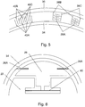
- FIG 2 schematically shows a cross section view of an embodiment of the invention.
- This cross section view includes a cross section view of gyroscope wafer 20 of Figure 1 along line I.
- Gyroscope wafer 20 of Figure 1 is preferably affixed to a cap wafer 42 and to a reference wafer 44 such that gyroscope wafer 20 is sandwiched in between cap wafer 42 and reference wafer 44 as shown on Figure 2 .
- cap wafer 42 and reference wafer 44 combine to protect gyroscope wafer 20 from an ambient environment, thereby increasing the reliability and ruggedness of the sensor.
- the bonds in between gyroscope wafer 20 and wafers 42 and 44 can be made so as to provide a hermetic barrier in between critical elements of gyroscope wafer 20, such as the moving masses 22 and 24, and the ambient environment.
- Cap wafer 42 and reference wafer 44 are attached to base 36 of gyroscope wafer 20, and do not make contact with any other component of gyroscope wafer 20, as shown on Figure 2 . Since flexures 32 and frame 34 make no contact with cap wafer 42, or with reference wafer 44, these wafers do not interfere with rotation of frame 34 about the Z axis.
- the connection between reference wafer 44 and base 36 is schematically indicated as 46 on Figure 2 .
- Connection 46 is both a mechanical connection between reference wafer 44 and base 36 and an electrical connection between reference wafer 44 and base 36. In this manner, circuitry on reference wafer 44 is connected to sense/drive means on gyroscope wafer 20, such as electrodes 38A, 38B, 38C or electrodes 40A, 40B, 40C on Figure 5 .
- Electrodes 48A and 48B are positioned on reference wafer 44 beneath plate 30. Electrodes 48A and 48B are positioned on either side of the rotation axis of plate 30, indicated as point 30B on Figure 2 . Similarly, electrodes 50A and 50B are positioned beneath plate 28, and electrodes 52A and 52B are positioned beneath plate 26.
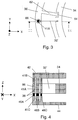
- FIG 3 schematically shows a more detailed plan view of a preferred configuration for flexure 32 on Figure 1 .
- flexure 32 comprises a spring 32' and a base flexure mount 66.
- the attachment point of spring 32' to mount 66 is recessed into mount 66, and similarly for frame 34, to reduce the coupling of surface stresses from mount 66 to spring 32' and from frame 34 to spring 32'.
- Base flexure mount 66 is surrounded by a base isolation trench 41A, which serves to mechanically isolate flexure 32 from stresses within base 36. Such stresses can be transmitted to base 36 by cap wafer 42 and reference wafer 44 as a result of packaging and/or bonding processes, thermal expansion, etc.
- a base tab 62 is also shown on Figure 3 , which is engaged with a frame groove 64. Frame groove 64 is somewhat larger than the width of base tab 62, as schematically indicated on Figure 3 , so that frame 34 can rotate only within a certain selected range relative to base 36 before base tab 62 collides with a wall of frame groove 64. This selected range is chosen to ensure that flexure 32 is not damaged by motion within the selected range. In this manner, the combination of tab 62 and groove 64 provides protection for flexure 32.
- FIG. 4 Further details of a preferred configuration for flexure 32 are shown in the cross section view of Figure 4 , which includes a cross section view of Figure 3 along line II. Line II is immediately adjacent to spring 32', but does not cut through it, which is why spring 32' is not shown as a cross section on Figure 4 .
- Base flexure mount 66 is affixed to cap wafer 42 and is connected to reference wafer 44 via a connection 46B. In this manner, flexure 32 is connected to cap wafer 42 and reference wafer 44, and isolation from base 36. This is advantageous because cap wafer 42 and reference wafer 44 are typically much thicker than base 36 (a typical thickness for gyroscope wafer 20 is only 50 microns), and therefore provide much greater mechanical rigidity for anchoring flexure 32.
- Reference isolation trench 41C serves to isolate flexure 32 from stresses which may be present in the top surface of reference wafer 44 (i.e., the surface of reference wafer 44 that is bonded to base 36).
- cap isolation trench 41B serves to isolate flexure 32 from stresses which may be present in the bottom surface of cap wafer 42 (i.e., the surface of cap wafer 42 that is bonded to base 36).
- FIG. 6 schematically shows an enlarged plan view of a portion of gyroscope wafer 20, which shows a preferred configuration of torsional hinges 26A and flexure hinge 60 in greater detail.
- plate 26 is attached to frame 34 by torsional hinges 26A.
- the configuration of torsional hinges 26A is such that plate 26 can rotate about the axis connecting the centers of torsional hinges 26A.
- slots are formed in plate 26 to increase the length of torsional hinges 26A. This is done in order to reduce the strain required on torsional hinges 26A to accommodate a given rotation of plate 26.
- Plate 26 is connected to mass 22 with flexure hinge 60.
- the configuration of flexure hinge 60 is such that plate 22 can tilt relative to mass 26 (and vice versa).
- a slot is formed in mass 22 to increase the length of flexure hinge 60, in order to reduce the strain required on flexure hinge 60 to accommodate a given tilt of mass 22 with respect to plate 26.
- flexure hinges 58, 56, and 54 are preferably similar to the configuration shown on Figure 6 for flexure hinge 60.
- the configurations of torsional hinges 28A and 30A are preferably similar to the configuration shown on Figure 6 for torsional hinge 26A.
- the hinge configurations shown in Figure 6 pertain to a preferred embodiment of the invention. Practice of the invention does not require any particular hinge configuration.
- the embodiment of Figures 1 and 2 has two modes of operation. In a first and preferred mode of operation, masses 22 and 24 are driven into oscillation and the motion of frame 34 is sensed to measure Y-directed angular velocity. In a second mode of operation, frame 34 is driven into oscillation and the motion of masses 22 and 24 is sensed to measure Y-directed angular velocity. These two methods will be considered in turn.
- the first preferred mode of operation includes an actuator for driving the linkage into oscillation.
- an electrostatic actuator is provided by electrodes 48A, 48B, 50A, 50B, 52A and 52B of Figure 2 .
- Electrodes 48A, 48B, 50A, 50B, 52A and 52B interact with plates 30, 28 and 26 via an electrostatic interaction, where the force increases as the potential difference between the electrode and the corresponding plate increases. Plates 26, 28 and 30 are typically held at the same electric potential, which can be taken to be the zero reference for electric potential without loss of generality.
- Electrodes 48A, 48B, 50A, 50B, 52A and 52B are preferably split electrodes, as shown on Figure 2 .
- the main reason for this is that the electrostatic interaction between a plate and an electrode tends to be an attraction (instead of a repulsion), so to provide torques in either direction, an electrode element on either side of the rotation axis is required, as shown on Figure 2 .
- the gap between electrodes 48A, 48B, 50A, 50B, 52A and 52B, and the corresponding plates (30, 28 and 26 respectively) is preferably precisely controlled in fabrication to a gap height d, to reduce the voltage required to obtain a given rotation of the plates as much as possible, while still providing adequate clearance for the movement of actuators.
- Electrodes 48A, 48B, 50A, 50B, 52A and 52B are preferably electrically driven in a cooperative manner to excite an oscillation mode of the linkage formed by masses 22 and 24, and plates 26, 28, and 30 having oscillation of masses 22 and 24, substantially out of phase with each other, in the Z direction (i.e., out of plane direction).
- the linkage motion corresponding to this oscillation mode is schematically shown on Figures 11a and 11b .
- plate 26 it is also preferable for plate 26 to include a lever arm extending toward mass 22, for plate 30 to include a lever arm extending toward mass 24, and for plate 28 to include lever arms extending toward both mass 22 and mass 24, all as shown on Figure 1 .
- the lever arms extending from plates 26, 28 and 30 the distance between the flexure hinges (54, 56, 58, 60) and the axes of plate rotation (26B, 28B, 30B) is increased, which increases the displacement of masses 22 and 24 provided by a given rotation of the plates.
- Such increased displacement is highly desirable for improving gyroscope performance and/or for providing a desired level of performance at a lower cost.
- recesses 45 and 47 are formed in reference wafer 44 beneath masses 22 and 24, respectively.
- Cap wafer 42 is also configured to allow sufficient room to accommodate all moving parts of gyroscope wafer 20.
- the linkage containing masses 22 and 24 it is preferable to exploit mechanical resonances of the gyroscope structure. Accordingly, it is preferable to drive the linkage containing masses 22 and 24 at a frequency which is equal or about equal to the fundamental linkage resonant mode frequency.
- the fundamental linkage resonant mode i.e., the mechanical mode having lowest frequency
- the fundamental linkage resonant mode will correspond to antiphase oscillation of masses 22 and 24 as shown in Figures 11a and 11b .
- Such correspondence can be ensured during design of the linkage and its supporting flexures.
- the fundamental frame resonant mode corresponds to rigid body angular oscillation of frame 34 about the Z axis, which can be done by suitable design of frame 34 and flexures 32.
- the frame fundamental frequency it is preferable for the frame fundamental frequency to be greater than the linkage fundamental frequency. This ensures that the drive frequency is closer in frequency to the fundamental mode of frame 34 than to any other resonant mode of frame 34, thereby minimizing the excitation of higher order mechanical modes of frame 34 which can interfere with gyroscope operation.
- the angular oscillation amplitude of frame 34 is sensed with a transducer.
- the transducer is a capacitive sensor disposed between and connected to frame 34 and base 36.
- Two suitable electrode configurations for such a capacitive sensor are shown on Figure 5 .
- the configuration shown as 38A, 38B and 38C on Figure 5 is referred to as a tree configuration, while the configuration shown as 40A, 40B and 40C on Figure 5 is referred to as a radial configuration.
- electrodes 38A are attached to and move with frame 34, while electrodes 38B and 38C are both attached to base 36 and do not move with frame 34.
- the "unit cell” consisting of one electrode 38A, one electrode 38B and one electrode 38C can be repeated as desired in the region between frame 34 and base 36. Two such “unit cells” are shown on Figure 5 . Electrically, all electrodes 38A are connected to each other, all electrodes 38B are connected to each other, and all electrodes 38C are connected to each other. Thus two capacitors are formed: capacitor AB between electrodes 38A and 38B, and capacitor AC between electrodes 38A and 38C. Such an arrangement, where electrodes 38B are not connected to electrodes 38C, is known as a split-finger configuration. Since motion of frame 34 changes the capacitance of capacitors AB and AC, measuring these capacitances with circuitry provides sensing of motion of frame 34. Such circuitry is preferably located on reference wafer 44.
- electrodes 40A are attached to and move with frame 34, while electrodes 40B and 40C are attached to base 36 and do not move with frame 34.
- two capacitors are formed, and measuring these capacitances with circuitry (preferably located on reference wafer 44) provides sensing of motion of frame 34.
- frame 34 is driven into angular oscillation about the Z axis, which entails antiphase oscillation of masses 22 and 24 along the X axis.
- gyroscope wafer 20 is rotated about the Y axis with angular velocity w y
- the oscillation of frame 34 induces oscillating Z-directed Coriolis forces on masses 22 and 24, which set the linkage including masses 22 and 24 into oscillation. Since the amplitude of the oscillation of the linkage depends on w y (ideally it is proportional to w y ), measuring this amplitude provides a measurement of the angular velocity w y .
- the second operation mode includes an actuator for driving frame 34 into angular oscillation.
- An electrostatic actuator connected to frame 34 and base 36 is one suitable means for driving frame 34 into angular oscillation.
- Such an electrostatic actuator may have various electrode configurations, including the configurations of Figure 5 .
- angular velocity sensors advantageously reduce errors induced by any linear acceleration the sensor may be subjected to.
- the motion that is sensed is an angular oscillation of frame 34, and linear acceleration of the sensor does not tend to induce such a motion.
- the motion that is sensed is an antiphase oscillation of masses 22 and 24, and here also the sensed motion is not a motion that linear acceleration tends to induce.
- linear Z directed acceleration tends to induce in-phase (as opposed to antiphase) oscillation of masses 22 and 24.
- an angular rotation sensor (or gyroscope) having the structure and operation discussed above is fabricated with micromachining technology (also known as MEMS technology).
- MEMS technology also known as MEMS technology.
- MEMS technology Two forms of MEMS technology are known: bulk MEMS and surface MEMS.
- Bulk MEMS technology is preferable for the present invention, because bulk MEMS proof masses (i.e. masses 22 and 24) can have greater mass and can have a larger range of motion than surface MEMS proof masses.
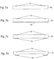
- Figures 7a-d, 8a-d, 9a-d and 10a,b schematically show an exemplary fabrication sequence suitable for fabricating an embodiment of the invention.
- Figures 7a-d schematically show a sequence of steps suitable for fabricating cap wafer 42.
- cap wafer 42 is patterned with backside alignment marks 72. Marks 72 can be made using reactive ion etching (RIE).
- RIE reactive ion etching
- the surface of cap wafer 42 facing away from alignment marks 72 is cleaned, and then thermally oxidized, to generate an oxide layer 70.
- Oxide layer 70 is preferably about 0.5 microns thick, and can be made by heating wafer 42' to a high temperature (e.g., greater than 1000 C) in a water-containing ambient environment.
- oxide layer 70 is lithographically patterned, as schematically shown on Figure 7c .
- cap wafer 42 In passing from Figure 7c to 7d , material of cap wafer 42 not protected by oxide layer 70 is etched away to a depth of about 100 microns. Deep RIE (DRIE) is a suitable etch method for this step. At this point in the process, cap wafer 42 has the configuration shown in Figure 2 . After the etch, cap wafer 42 is cleaned in preparation for a fusion bond. Suitable cleaning steps include a high temperature (> 300 C) ashing step and a sulfuric peroxide dip. The cleaning methods employed must leave patterned oxide layer 70 intact.
- DRIE Deep RIE
- FIGs 8a-d schematically show a sequence of processing steps suitable for fabricating gyroscope wafer 20.
- Gyroscope wafer 20 is preferably a prime low total thickness variation (TTV) wafer.
- Gyroscope wafer 20 is cleaned with a sulfuric peroxide dip and is then fusion bonded to patterned oxide layer 70 on cap wafer 42, as shown on Figure 8a .
- the bonding of cap wafer 42 to gyroscope wafer 20 occurs in an earlier stage of processing than the bonding of reference wafer 44 to gyroscope wafer 20.
- gyroscope wafer 20 is thinned from typically about 500 microns thickness to about 40 microns thickness. Conventional grinding and polishing is a suitable method for performing this thinning step.
- the thinning of gyroscope wafer 20 can be done uniformly, or it can be done so that regions of gyroscope wafer 20 that will become masses 22 and 24 are thicker than other parts of gyroscope wafer 20. Such increased thickness is beneficial because it increases the masses of masses 22 and 24.
- standoffs 71 shown on Figure 8b are formed by lithographic patterning followed by an etch. A KOH etch is suitable for this step. The purpose of standoffs 71 is to precisely determine the vertical separation d between actuator electrodes such as electrodes 48A,B, 50A,B and 52A,B on Figure 2 from the corresponding plates (i.e., plates 30, 28 and 26 respectively).
- a patterned layer 46' is deposited on gyroscope wafer 20.
- patterned layer 46' is a Ge layer which is deposited and then patterned (e.g., by lithography followed by an etch).
- patterned layer 46' also defines electrodes between frame 34 and base 36, which can be of the types shown in Figure 5 .
- electrodes between frame 34 and base 36 can be formed in a separate processing step from deposition of patterned layer 46'.
- the mechanical elements of gyroscope wafer 20 are formed by etching through gyroscope wafer 20.
- the pattern to be etched can be formed photolithographically.
- a 2 micron line width and 2 micron spacing is suitable for this etch, which stops on oxide layer 70.
- Deep RIE with Silicon-on-insulator (SOI) anti-footing enhancement is a suitable etch method for this step. It is preferable for this etching to be performed with an etching process suitable for creating high-aspect ratio features.
- all of the mechanical elements of gyroscope wafer 20, shown on Figures 1-4 and Figure 6 are formed. These elements include masses 22 and 24, plates 26, 28, and 30, flexures 32, frame 34, and hinges 26A, 28A, 30A, 54, 56, 58 and 60.
- Figure 8d only shows plate 28 and masses 22 and 24.
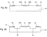
- FIGs 9a-b schematically show a sequence of processing steps suitable for fabricating reference wafer 44.
- the active areas of reference wafer 44 are schematically indicated as 74.
- Active areas 74 include regions that will make electrical contact with gyroscope wafer 20, as well as circuitry for driving gyroscope wafer 20 and circuitry for sensing output signals provided by gyroscope wafer 20.
- Such circuitry is preferably conventional Silicon CMOS circuitry.
- the last layer of metal deposited in the conventional CMOS process is a metal layer suitable for use as a bond metal.
- This upper layer of metal also defines the electrodes 48A,B, 50A,B and 52A,B (only electrodes 50A,B are shown on Figure 9b ), and bond pads 76, schematically shown on Figure 9a .
- recesses 45 and 47 are formed in reference wafer 44. Recesses 45 and 47 are preferably fabricated with DRIE, to a depth of about 100 microns.
- FIGs 10a-b schematically show a sequence of processing steps suitable for final assembly of gyroscope wafer 20, reference wafer 44 and cap wafer 42.
- reference wafer 44 is shown attached to gyroscope wafer 20 via an aligned metal to metal bond between patterned layer 46' on gyroscope wafer 20, and bond pads 76 on reference wafer 44.
- the bonding of reference wafer 44 to gyroscope wafer 20 occurs in a later stage of processing than the bonding of cap wafer 42 to gyroscope wafer 20.
- relatively low temperature bonding processes are preferred for bonding reference wafer 44 to gyroscope wafer 20, including but not limited to: eutectic metal bonding, Aluminum-Germanium bonding, solder bonding, Indium-Gold bonding, and polymer bonding.
- the separation d between plate 28 and electrodes 50A and 50B on Figure 10a is determined by the combined thickness of standoffs 71 and patterned layer 46', and can be precisely controlled (or predetermined) by selecting the height of standoffs 71.
- the separation between other electrodes (e.g., electrodes 48A,B and electrodes 52A,B) and their corresponding plates (e.g., plates 30 and 26 respectively) is also determined in the same way, and typically the same predetermined distance d separates all plates from their corresponding electrodes.
- FIG. 7-10 shows standoffs 71 being formed exclusively on gyroscope wafer 20, it is also possible to form standoffs exclusively on reference wafer 44, or on both gyroscope wafer 20 and reference wafer 44 in order to define the separation between plates and electrodes.
- material is etched away from cap wafer 42 to allow access to active areas 74 from above. This etch can be done with DRIE. By allowing access to active areas 74 from above, electrical connection to the angular velocity sensor of Figure 10b is facilitated.
- Reference wafer 44 is preferably attached to gyroscope wafer 20 via a metal-to-metal bond, which can be made hermetic.
- gyroscope wafer 20 is preferably attached to cap wafer 42 by a fusion bond, which can also be made hermetic.
- the entire assembly of reference wafer 44, gyroscope wafer 20 and cap wafer 42 can provide a hermetic barrier between gyroscope elements (such as masses 22 and 24) and an ambient environment.
- a reduced pressure e.g., about 1 mTorr, which is substantially less than atmospheric pressure
- a reduced pressure e.g., about 1 mTorr, which is substantially less than atmospheric pressure
- holes can be provided in masses 22 and 24 (and in other moving parts of the linkage) to reduce air resistance to motion.
- Figure 12 is a schematic top view of an alternate electrode configuration.
- masses 22 and 24, and plates 26, 28, and 30 are not shown, so that the electrodes beneath these elements of the linkage can be seen.
- electrodes 48A,B, 50A,B and 52A.,B serve to drive plates 30, 28, and 26 respectively, as described above.
- the configuration of Figure 12 provides electrodes 51A and 51B for sensing motion of the masses, or more generally, motion of the linkage. Signals provided by electrodes 51A and 51B can be advantageously used by circuitry which drives the linkage actuators. For example, sensing the motion of the linkage in this manner allows the driving circuitry to drive the linkage precisely at its fundamental mechanical resonance frequency.
- Figure 13 schematically shows a top view of an integrated dual-axis gyroscope according to an embodiment of the present invention.
- a Y-axis subsensor 20Y and an X-axis subsensor 20X are preferably fabricated on a single Silicon chip 21.
- Subsensors 20X and 20Y are preferably sensors as described in connection with Figures 1 and 2 , and the configuration of Figure 13 advantageously provides dual-axis sensing with an integrated angular velocity sensor.
- Such integration greatly reduces cost, compared to two non-integrated, single-axis sensors.
- Figures 14a and 14b schematically show a top view of an embodiment of the invention that provides further common-mode rejection of unwanted motion.
- the configurations of Figures 14a and 14b include two frames, frame 34A and frame 34B.
- Masses 22A and 24A are positioned within frame 34A and masses 22B and 24B are positioned within frame 34B in much the same way that masses 22 and 24 are positioned within frame 34 on Figure 1 .
- Masses 22A,B and 24A,B on Figures 14a and 14b are driven into oscillation such that masses 24A and 22B are in phase.
- Masses 22A and 24A are linked to move out of phase, as are masses 22B and 24B.
- Frames 34A and 34B are connected to each other by a flexure 32, and are connected to a base 36' by a plurality of flexures 32.
- the flexure configurations shown on Figures 14a and 14b are exemplary, and the invention can be practiced with other flexure configurations.
- the connection of frame 34A to frame 34B by flexure 32 tends to inhibit in-phase rotation of frames 34A and 34B relative to out-of-phase rotation of frames 34A and 34B because in-phase rotation of frames 34A and 34B stretches flexure 32 more than out-of-phase rotation of the same magnitude.
- the embodiments of Figures 14a and 14b have zero net linear and angular momentum in the driven linkages, while the embodiment of Figure 1 has zero net linear momentum but nonzero net angular momentum in the driven linkage. Since transfer of vibration to the sensor package tends to decrease when the driven linkage has zero net linear or angular momentum, the embodiments of Figures 14a and 14b should provide reduced package vibration compared to the embodiment of Figure 1 . Reduced vibration can result in reduced measurement errors, such as bias errors and quadrature errors.
- frames 34A and 34B In order to maximize the benefit of the common mode rejection of Z-directed angular acceleration provided by the embodiments of Figures 14a and 14b , it is preferable for frames 34A and 34B to have substantially the same shape, and for the linkages within frames 34A and 34B to have substantially the same configuration and orientation. This level of symmetry provides motions responsive to Y-directed angular velocity that are substantially equal and opposite, which maximizes the rejection of motions not responsive to Y-directed angular velocity (e.g., motions due to Z-directed angular acceleration).
- Figure 15 schematically shows an alternate embodiment of the invention, where frame 34 and base 36 are rectangular instead of circular.
- masses 22 and 24 are linked together by plates 26, 28, and 30, similar to the embodiment of Figure 1 .
- the linkage including masses 22 and 24, and plates 26, 28, and 30 is preferably driven into oscillation by electrostatic actuators (not shown on Figure 15 ). Rotation of the embodiment of Figure 15 about the Y axis will induce X-directed Coriolis forces on masses 22 and 24.
- Frame 34 is connected to base 36 with a plurality of flexures 32 which permit frame 34 to move relative to base 36.
- frame 34 and flexures 32 on Figure 15 inhibits overall rotation of frame 34 and senses X directed deformation of frame 34 responsive to Y-directed angular velocity.
- An alternate configuration of frame 34 and flexures 32 on Figure 15 can also be employed, which inhibits X-directed deformation (e.g., by making frame 34 stiffer), and senses rotation of frame 34.
- Figures 16a and 16b show examples of alternative configurations for flexures 32 between frame 34 and base 36.
- Figure 16a shows an arrangement of flexures 32 that is rotated by 45 degrees relative to the arrangement of flexures 32 shown on Figure 1 .
- Figure 16b shows an arrangement of three flexures 32 symmetrically disposed between frame 34 and base 36.
- the invention can be practiced with any arrangement of flexures between frame 34 and base 36 that permit frame 34 to move relative to base 36 responsive to the angular velocity to be sensed.
- an actuator for driving the linkage into oscillation being an electrostatic actuator
- Alternate actuators for driving the linkage into oscillation include but are not limited to, electromagnetic actuators, piezoelectric actuators and thermal actuators.
- a transducer for sensing angular oscillation of frame 34 being a capacitive sensor was disclosed.
- Alternate transducers for sensing angular oscillation of frame 34 include but are not limited to, electromagnetic sensors, piezoresistive sensors, and piezoelectric sensors.
- an actuator for driving frame 34 into angular oscillation being an electrostatic actuator
- Alternate actuators for driving frame 34 into oscillation include but are not limited to, electromagnetic actuators, piezoelectric actuators and thermal actuators.
- a transducer for sensing oscillation of the linkage being a capacitive sensor was disclosed.
- Alternate transducers for sensing oscillation of the linkage include but are not limited to, electromagnetic sensors, piezoresistive sensors, and piezoelectric sensors.
Landscapes
- Physics & Mathematics (AREA)
- Engineering & Computer Science (AREA)
- General Physics & Mathematics (AREA)
- Radar, Positioning & Navigation (AREA)
- Remote Sensing (AREA)
- Gyroscopes (AREA)
Applications Claiming Priority (2)
| Application Number | Priority Date | Filing Date | Title |
|---|---|---|---|
| US10/690,224 US6892575B2 (en) | 2003-10-20 | 2003-10-20 | X-Y axis dual-mass tuning fork gyroscope with vertically integrated electronics and wafer-scale hermetic packaging |
| PCT/US2004/034431 WO2005043079A2 (en) | 2003-10-20 | 2004-10-12 | X-y axis dual-mass tuning fork gyroscope with vertically integrated electronics and wafer-scale hermetic packaging |
Publications (3)
| Publication Number | Publication Date |
|---|---|
| EP1676096A2 EP1676096A2 (en) | 2006-07-05 |
| EP1676096A4 EP1676096A4 (en) | 2009-11-18 |
| EP1676096B1 true EP1676096B1 (en) | 2017-06-07 |
Family
ID=34521583
Family Applications (1)
| Application Number | Title | Priority Date | Filing Date |
|---|---|---|---|
| EP04795573.7A Expired - Lifetime EP1676096B1 (en) | 2003-10-20 | 2004-10-12 | X-y axis dual-mass tuning fork gyroscope with vertically integrated electronics and wafer-scale hermetic packaging |
Country Status (5)
| Country | Link |
|---|---|
| US (1) | US6892575B2 (enExample) |
| EP (1) | EP1676096B1 (enExample) |
| JP (1) | JP5021312B2 (enExample) |
| TW (1) | TWI247896B (enExample) |
| WO (1) | WO2005043079A2 (enExample) |
Families Citing this family (120)
| Publication number | Priority date | Publication date | Assignee | Title |
|---|---|---|---|---|
| US7458263B2 (en) * | 2003-10-20 | 2008-12-02 | Invensense Inc. | Method of making an X-Y axis dual-mass tuning fork gyroscope with vertically integrated electronics and wafer-scale hermetic packaging |
| KR100652952B1 (ko) * | 2004-07-19 | 2006-12-06 | 삼성전자주식회사 | 커플링 스프링을 구비한 멤스 자이로스코프 |
| FR2876180B1 (fr) * | 2004-10-06 | 2006-12-08 | Commissariat Energie Atomique | Resonateur a masses oscillantes. |
| FI116544B (fi) * | 2004-12-31 | 2005-12-15 | Vti Technologies Oy | Värähtelevä mikromekaaninen kulmanopeusanturi |
| FI116543B (fi) * | 2004-12-31 | 2005-12-15 | Vti Technologies Oy | Värähtelevä mikromekaaninen kulmanopeusanturi |
| US7442570B2 (en) | 2005-03-18 | 2008-10-28 | Invensence Inc. | Method of fabrication of a AL/GE bonding in a wafer packaging environment and a product produced therefrom |
| US7240552B2 (en) * | 2005-06-06 | 2007-07-10 | Bei Technologies, Inc. | Torsional rate sensor with momentum balance and mode decoupling |
| US7621183B2 (en) * | 2005-11-18 | 2009-11-24 | Invensense Inc. | X-Y axis dual-mass tuning fork gyroscope with vertically integrated electronics and wafer-scale hermetic packaging |
| EP2899502B1 (en) | 2006-01-24 | 2017-04-05 | Panasonic Corporation | Inertial force sensor |
| JP4974340B2 (ja) * | 2006-05-15 | 2012-07-11 | 住友精密工業株式会社 | 角速度センサ |
| JP4310325B2 (ja) * | 2006-05-24 | 2009-08-05 | 日立金属株式会社 | 角速度センサ |
| US7434464B2 (en) * | 2006-09-29 | 2008-10-14 | Freescale Semiconductor, Inc. | Methods and apparatus for a MEMS gyro sensor |
| DE102006046772A1 (de) * | 2006-09-29 | 2008-04-03 | Siemens Ag | Anordnung zur Messung einer Drehrate mit einem Vibrationssensor |
| US7461552B2 (en) * | 2006-10-23 | 2008-12-09 | Custom Sensors & Technologies, Inc. | Dual axis rate sensor |
| JP4942470B2 (ja) * | 2006-12-20 | 2012-05-30 | 住友精密工業株式会社 | 2軸角速度センサ |
| US8250921B2 (en) | 2007-07-06 | 2012-08-28 | Invensense, Inc. | Integrated motion processing unit (MPU) with MEMS inertial sensing and embedded digital electronics |
| US8508039B1 (en) * | 2008-05-08 | 2013-08-13 | Invensense, Inc. | Wafer scale chip scale packaging of vertically integrated MEMS sensors with electronics |
| US8462109B2 (en) | 2007-01-05 | 2013-06-11 | Invensense, Inc. | Controlling and accessing content using motion processing on mobile devices |
| US7796872B2 (en) * | 2007-01-05 | 2010-09-14 | Invensense, Inc. | Method and apparatus for producing a sharp image from a handheld device containing a gyroscope |
| US20090262074A1 (en) * | 2007-01-05 | 2009-10-22 | Invensense Inc. | Controlling and accessing content using motion processing on mobile devices |
| US8047075B2 (en) | 2007-06-21 | 2011-11-01 | Invensense, Inc. | Vertically integrated 3-axis MEMS accelerometer with electronics |
| US8020441B2 (en) | 2008-02-05 | 2011-09-20 | Invensense, Inc. | Dual mode sensing for vibratory gyroscope |
| US20090265671A1 (en) * | 2008-04-21 | 2009-10-22 | Invensense | Mobile devices with motion gesture recognition |
| US8141424B2 (en) | 2008-09-12 | 2012-03-27 | Invensense, Inc. | Low inertia frame for detecting coriolis acceleration |
| US20100071467A1 (en) * | 2008-09-24 | 2010-03-25 | Invensense | Integrated multiaxis motion sensor |
| US8952832B2 (en) | 2008-01-18 | 2015-02-10 | Invensense, Inc. | Interfacing application programs and motion sensors of a device |
| US7934423B2 (en) | 2007-12-10 | 2011-05-03 | Invensense, Inc. | Vertically integrated 3-axis MEMS angular accelerometer with integrated electronics |
| JP4792143B2 (ja) * | 2007-02-22 | 2011-10-12 | 株式会社デンソー | 半導体装置およびその製造方法 |
| RU2445635C2 (ru) * | 2007-04-13 | 2012-03-20 | Кинетик, Инк. | Силовой датчик и способ определения радиуса поворота движущегося объекта |
| KR100856293B1 (ko) * | 2007-05-04 | 2008-09-03 | 삼성전기주식회사 | 수정 진동자 제조방법 |
| EP2011762B1 (en) * | 2007-07-02 | 2015-09-30 | Denso Corporation | Semiconductor device with a sensor connected to an external element |
| US20090085194A1 (en) * | 2007-09-28 | 2009-04-02 | Honeywell International Inc. | Wafer level packaged mems device |
| US7677099B2 (en) * | 2007-11-05 | 2010-03-16 | Invensense Inc. | Integrated microelectromechanical systems (MEMS) vibrating mass Z-axis rate sensor |
| US8089518B2 (en) * | 2007-11-16 | 2012-01-03 | Samsung Electronics Co., Ltd. | System and method for automatic image capture in a handheld camera with a multiple-axis actuating mechanism |
| US8125512B2 (en) * | 2007-11-16 | 2012-02-28 | Samsung Electronics Co., Ltd. | System and method for moving object selection in a handheld image capture device |
| JP5450451B2 (ja) * | 2008-02-05 | 2014-03-26 | インベンセンス,インク. | 垂直方向に集積した電子回路およびウェハスケール密封包装を含むx−y軸二重質量音叉ジャイロスコープ |
| US7971483B2 (en) * | 2008-03-28 | 2011-07-05 | Honeywell International Inc. | Systems and methods for acceleration and rotational determination from an out-of-plane MEMS device |
| US7984648B2 (en) | 2008-04-10 | 2011-07-26 | Honeywell International Inc. | Systems and methods for acceleration and rotational determination from an in-plane and out-of-plane MEMS device |
| US8011247B2 (en) * | 2008-06-26 | 2011-09-06 | Honeywell International Inc. | Multistage proof-mass movement deceleration within MEMS structures |
| KR101001666B1 (ko) * | 2008-07-08 | 2010-12-15 | 광주과학기술원 | 마이크로 수직 구조체의 제조 방법 |
| US8682606B2 (en) * | 2008-10-07 | 2014-03-25 | Qualcomm Incorporated | Generating virtual buttons using motion sensors |
| JP2010117292A (ja) * | 2008-11-14 | 2010-05-27 | Alps Electric Co Ltd | 角速度センサ |
| DE102008043796B4 (de) * | 2008-11-17 | 2023-12-21 | Robert Bosch Gmbh | Drehratensensor |
| US8351910B2 (en) * | 2008-12-02 | 2013-01-08 | Qualcomm Incorporated | Method and apparatus for determining a user input from inertial sensors |
| DE102009001244A1 (de) * | 2009-02-27 | 2010-09-02 | Sensordynamics Ag | Mikro-Gyroskop zur Ermittlung von Rotationsbewegungen um eine x-, y- oder z-Achse |
| FI20095201A0 (fi) * | 2009-03-02 | 2009-03-02 | Vti Technologies Oy | Värähtelevä mikromekaaninen kulmanopeusanturi |
| US8151641B2 (en) | 2009-05-21 | 2012-04-10 | Analog Devices, Inc. | Mode-matching apparatus and method for micromachined inertial sensors |
| US8266961B2 (en) * | 2009-08-04 | 2012-09-18 | Analog Devices, Inc. | Inertial sensors with reduced sensitivity to quadrature errors and micromachining inaccuracies |
| WO2011019702A1 (en) * | 2009-08-13 | 2011-02-17 | Analog Devices, Inc. | Mems in-plane resonators |
| US8783103B2 (en) * | 2009-08-21 | 2014-07-22 | Analog Devices, Inc. | Offset detection and compensation for micromachined inertial sensors |
| EP2475959B1 (de) | 2009-09-09 | 2015-07-08 | Continental Teves AG & Co. oHG | Doppelaxialer, schockrobuster, drehratensensor mit linearen und rotatorischen seismischen elementen |
| US8534127B2 (en) * | 2009-09-11 | 2013-09-17 | Invensense, Inc. | Extension-mode angular velocity sensor |
| US9097524B2 (en) * | 2009-09-11 | 2015-08-04 | Invensense, Inc. | MEMS device with improved spring system |
| US8701459B2 (en) * | 2009-10-20 | 2014-04-22 | Analog Devices, Inc. | Apparatus and method for calibrating MEMS inertial sensors |
| US8516887B2 (en) * | 2010-04-30 | 2013-08-27 | Qualcomm Mems Technologies, Inc. | Micromachined piezoelectric z-axis gyroscope |
| US8966400B2 (en) | 2010-06-07 | 2015-02-24 | Empire Technology Development Llc | User movement interpretation in computer generated reality |
| TWI434803B (zh) | 2010-06-30 | 2014-04-21 | Ind Tech Res Inst | 微機電元件與電路晶片之整合裝置及其製造方法 |
| US8395381B2 (en) | 2010-07-09 | 2013-03-12 | Invensense, Inc. | Micromachined magnetic field sensors |
| US20120007597A1 (en) * | 2010-07-09 | 2012-01-12 | Invensense, Inc. | Micromachined offset reduction structures for magnetic field sensing |
| US8567246B2 (en) | 2010-10-12 | 2013-10-29 | Invensense, Inc. | Integrated MEMS device and method of use |
| US8631700B2 (en) | 2010-11-05 | 2014-01-21 | Analog Devices, Inc. | Resonating sensor with mechanical constraints |
| US8616056B2 (en) | 2010-11-05 | 2013-12-31 | Analog Devices, Inc. | BAW gyroscope with bottom electrode |
| US9091544B2 (en) | 2010-11-05 | 2015-07-28 | Analog Devices, Inc. | XY-axis shell-type gyroscopes with reduced cross-talk sensitivity and/or mode matching |
| US8604663B2 (en) * | 2010-11-15 | 2013-12-10 | DigitalOptics Corporation MEMS | Motion controlled actuator |
| DE102010062056B4 (de) | 2010-11-26 | 2018-09-27 | Robert Bosch Gmbh | Mikromechanisches Bauteil |
| EP2646773B1 (en) | 2010-12-01 | 2015-06-24 | Analog Devices, Inc. | Apparatus and method for anchoring electrodes in mems devices |
| US9664750B2 (en) | 2011-01-11 | 2017-05-30 | Invensense, Inc. | In-plane sensing Lorentz force magnetometer |
| US8860409B2 (en) | 2011-01-11 | 2014-10-14 | Invensense, Inc. | Micromachined resonant magnetic field sensors |
| US8947081B2 (en) | 2011-01-11 | 2015-02-03 | Invensense, Inc. | Micromachined resonant magnetic field sensors |
| JP5790915B2 (ja) * | 2011-01-13 | 2015-10-07 | セイコーエプソン株式会社 | 物理量センサー及び電子機器 |
| US9039976B2 (en) | 2011-01-31 | 2015-05-26 | Analog Devices, Inc. | MEMS sensors with closed nodal anchors for operation in an in-plane contour mode |
| JP5807381B2 (ja) * | 2011-05-20 | 2015-11-10 | セイコーエプソン株式会社 | 物理量センサー、および電子機器 |
| US9705450B2 (en) * | 2011-06-24 | 2017-07-11 | The United States Of America As Represented By The Secretary Of The Navy | Apparatus and methods for time domain measurement of oscillation perturbations |
| US20130001710A1 (en) * | 2011-06-29 | 2013-01-03 | Invensense, Inc. | Process for a sealed mems device with a portion exposed to the environment |
| EP2544370B1 (en) * | 2011-07-06 | 2020-01-01 | Nxp B.V. | MEMS resonator |
| US10914584B2 (en) | 2011-09-16 | 2021-02-09 | Invensense, Inc. | Drive and sense balanced, semi-coupled 3-axis gyroscope |
| US9863769B2 (en) | 2011-09-16 | 2018-01-09 | Invensense, Inc. | MEMS sensor with decoupled drive system |
| US8833162B2 (en) * | 2011-09-16 | 2014-09-16 | Invensense, Inc. | Micromachined gyroscope including a guided mass system |
| US9714842B2 (en) * | 2011-09-16 | 2017-07-25 | Invensense, Inc. | Gyroscope self test by applying rotation on coriolis sense mass |
| US9170107B2 (en) * | 2011-09-16 | 2015-10-27 | Invensense, Inc. | Micromachined gyroscope including a guided mass system |
| US8739627B2 (en) | 2011-10-26 | 2014-06-03 | Freescale Semiconductor, Inc. | Inertial sensor with off-axis spring system |
| DE102011056971A1 (de) * | 2011-12-23 | 2013-06-27 | Maxim Integrated Products, Inc. | Mikromechanischer Coriolis-Drehratensensor |
| TWI453371B (zh) | 2011-12-30 | 2014-09-21 | Ind Tech Res Inst | 一種具振盪模組的微機電系統裝置 |
| DE102012200132A1 (de) | 2012-01-05 | 2013-07-11 | Robert Bosch Gmbh | Drehratensensor und Verfahren zum Betrieb eines Drehratensensors |
| US8984942B2 (en) * | 2012-02-10 | 2015-03-24 | Hewlett-Packard Development Company, L.P. | Suspended masses in micro-mechanical devices |
| JP5708535B2 (ja) * | 2012-03-13 | 2015-04-30 | 株式会社デンソー | 角速度センサ |
| US9212908B2 (en) | 2012-04-26 | 2015-12-15 | Analog Devices, Inc. | MEMS gyroscopes with reduced errors |
| US9194704B2 (en) | 2013-03-13 | 2015-11-24 | Freescale Semiconductor, Inc. | Angular rate sensor having multiple axis sensing capability |
| WO2015042700A1 (en) | 2013-09-24 | 2015-04-02 | Motion Engine Inc. | Mems components and method of wafer-level manufacturing thereof |
| EP3019442A4 (en) | 2013-07-08 | 2017-01-25 | Motion Engine Inc. | Mems device and method of manufacturing |
| EP3028007A4 (en) | 2013-08-02 | 2017-07-12 | Motion Engine Inc. | Mems motion sensor and method of manufacturing |
| US9709595B2 (en) | 2013-11-14 | 2017-07-18 | Analog Devices, Inc. | Method and apparatus for detecting linear and rotational movement |
| US9599471B2 (en) | 2013-11-14 | 2017-03-21 | Analog Devices, Inc. | Dual use of a ring structure as gyroscope and accelerometer |
| JP6590812B2 (ja) | 2014-01-09 | 2019-10-16 | モーション・エンジン・インコーポレーテッド | 集積memsシステム |
| US9958271B2 (en) | 2014-01-21 | 2018-05-01 | Invensense, Inc. | Configuration to reduce non-linear motion |
| JP2015184009A (ja) | 2014-03-20 | 2015-10-22 | セイコーエプソン株式会社 | 振動素子、電子機器、および移動体 |
| US20170030788A1 (en) | 2014-04-10 | 2017-02-02 | Motion Engine Inc. | Mems pressure sensor |
| WO2015184531A1 (en) | 2014-06-02 | 2015-12-10 | Motion Engine Inc. | Multi-mass mems motion sensor |
| JP6481294B2 (ja) | 2014-09-05 | 2019-03-13 | セイコーエプソン株式会社 | 物理量センサー素子、物理量センサー、電子機器および移動体 |
| JP2016057073A (ja) | 2014-09-05 | 2016-04-21 | セイコーエプソン株式会社 | 物理量センサー素子、物理量センサー、電子機器および移動体 |
| JP6481293B2 (ja) | 2014-09-05 | 2019-03-13 | セイコーエプソン株式会社 | 物理量センサー素子、物理量センサー、電子機器および移動体 |
| WO2016040018A1 (en) | 2014-09-08 | 2016-03-17 | Invensense Incorporated | System and method for hierarchical sensor processing |
| US10746548B2 (en) | 2014-11-04 | 2020-08-18 | Analog Devices, Inc. | Ring gyroscope structural features |
| CA3004760A1 (en) | 2014-12-09 | 2016-06-16 | Motion Engine Inc. | 3d mems magnetometer and associated methods |
| US10231337B2 (en) | 2014-12-16 | 2019-03-12 | Inertial Sense, Inc. | Folded printed circuit assemblies and related methods |
| CA3004763A1 (en) | 2015-01-15 | 2016-07-21 | Motion Engine Inc. | 3d mems device with hermetic cavity |
| KR101659207B1 (ko) | 2015-02-05 | 2016-09-22 | 삼성전기주식회사 | 각속도 센서 |
| EP3257074A1 (en) | 2015-02-11 | 2017-12-20 | InvenSense, Inc. | 3D INTEGRATION USING Al-Ge EUTECTIC BOND INTERCONNECT |
| US9869552B2 (en) * | 2015-03-20 | 2018-01-16 | Analog Devices, Inc. | Gyroscope that compensates for fluctuations in sensitivity |
| KR101915954B1 (ko) * | 2016-06-29 | 2018-11-08 | 주식회사 신성씨앤티 | 멤스 기반의 3축 가속도 센서 |
| US10192850B1 (en) | 2016-09-19 | 2019-01-29 | Sitime Corporation | Bonding process with inhibited oxide formation |
| JP6639377B2 (ja) | 2016-12-08 | 2020-02-05 | 株式会社東芝 | 振動装置 |
| DE102017200725A1 (de) | 2017-01-18 | 2018-07-19 | Robert Bosch Gmbh | Mikromechanischer Sensor |
| US10466053B2 (en) * | 2017-04-04 | 2019-11-05 | Invensense, Inc. | Out-of-plane sensing gyroscope robust to external acceleration and rotation |
| US11656077B2 (en) | 2019-01-31 | 2023-05-23 | Analog Devices, Inc. | Pseudo-extensional mode MEMS ring gyroscope |
| EP3696503B1 (en) * | 2019-02-15 | 2022-10-26 | Murata Manufacturing Co., Ltd. | Vibration-robust multiaxis gyroscope |
| US11060866B2 (en) * | 2019-02-15 | 2021-07-13 | Murata Manufacturing Co., Ltd. | Balanced multiaxis gyroscope |
| DE102020205372A1 (de) * | 2020-04-28 | 2021-10-28 | Robert Bosch Gesellschaft mit beschränkter Haftung | Mikromechanisches Bauteil für einen Drehratensensor und entsprechendes Herstellungsverfahren |
| US11981560B2 (en) | 2020-06-09 | 2024-05-14 | Analog Devices, Inc. | Stress-isolated MEMS device comprising substrate having cavity and method of manufacture |
| US11714102B2 (en) | 2021-06-08 | 2023-08-01 | Analog Devices, Inc. | Fully differential accelerometer |
Family Cites Families (21)
| Publication number | Priority date | Publication date | Assignee | Title |
|---|---|---|---|---|
| US5359893A (en) * | 1991-12-19 | 1994-11-01 | Motorola, Inc. | Multi-axes gyroscope |
| DE4414237A1 (de) * | 1994-04-23 | 1995-10-26 | Bosch Gmbh Robert | Mikromechanischer Schwinger eines Schwingungsgyrometers |
| DE19523895A1 (de) * | 1995-06-30 | 1997-01-02 | Bosch Gmbh Robert | Beschleunigungssensor |
| US5992233A (en) | 1996-05-31 | 1999-11-30 | The Regents Of The University Of California | Micromachined Z-axis vibratory rate gyroscope |
| JPH1038578A (ja) * | 1996-07-17 | 1998-02-13 | Tokin Corp | 角速度センサ |
| US6122961A (en) | 1997-09-02 | 2000-09-26 | Analog Devices, Inc. | Micromachined gyros |
| JP3882973B2 (ja) * | 1998-06-22 | 2007-02-21 | アイシン精機株式会社 | 角速度センサ |
| JP3106395B2 (ja) * | 1998-07-10 | 2000-11-06 | 株式会社村田製作所 | 角速度センサ |
| US6481283B1 (en) | 1999-04-05 | 2002-11-19 | Milli Sensor Systems & Actuators, Inc. | Coriolis oscillating gyroscopic instrument |
| AU7049000A (en) | 1999-04-21 | 2000-11-21 | Regents Of The University Of California, The | Micro-machined angle-measuring gyroscope |
| US6189381B1 (en) * | 1999-04-26 | 2001-02-20 | Sitek, Inc. | Angular rate sensor made from a structural wafer of single crystal silicon |
| US6487907B1 (en) | 1999-07-08 | 2002-12-03 | California Institute Of Technology | Microgyroscope with integrated vibratory element |
| US6508122B1 (en) | 1999-09-16 | 2003-01-21 | American Gnc Corporation | Microelectromechanical system for measuring angular rate |
| KR100343211B1 (ko) | 1999-11-04 | 2002-07-10 | 윤종용 | 웨이퍼 레벨 진공 패키징이 가능한 mems의 구조물의제작방법 |
| WO2001071364A1 (en) | 2000-03-17 | 2001-09-27 | Microsensors, Inc. | Method of canceling quadrature error in an angular rate sensor |
| JP2002148048A (ja) * | 2000-11-08 | 2002-05-22 | Murata Mfg Co Ltd | 角速度検出素子 |
| US6480320B2 (en) | 2001-02-07 | 2002-11-12 | Transparent Optical, Inc. | Microelectromechanical mirror and mirror array |
| US6513380B2 (en) | 2001-06-19 | 2003-02-04 | Microsensors, Inc. | MEMS sensor with single central anchor and motion-limiting connection geometry |
| US6629460B2 (en) * | 2001-08-10 | 2003-10-07 | The Boeing Company | Isolated resonator gyroscope |
| KR100436367B1 (ko) | 2001-12-14 | 2004-06-19 | 삼성전자주식회사 | 수직 진동 질량체를 갖는 멤스 자이로스코프 |
| KR100431004B1 (ko) | 2002-02-08 | 2004-05-12 | 삼성전자주식회사 | 회전형 비연성 멤스 자이로스코프 |
-
2003
- 2003-10-20 US US10/690,224 patent/US6892575B2/en not_active Expired - Lifetime
-
2004
- 2004-10-12 EP EP04795573.7A patent/EP1676096B1/en not_active Expired - Lifetime
- 2004-10-12 WO PCT/US2004/034431 patent/WO2005043079A2/en not_active Ceased
- 2004-10-12 JP JP2006536699A patent/JP5021312B2/ja not_active Expired - Fee Related
- 2004-10-15 TW TW093131432A patent/TWI247896B/zh not_active IP Right Cessation
Also Published As
| Publication number | Publication date |
|---|---|
| US6892575B2 (en) | 2005-05-17 |
| JP2007509346A (ja) | 2007-04-12 |
| EP1676096A4 (en) | 2009-11-18 |
| EP1676096A2 (en) | 2006-07-05 |
| TWI247896B (en) | 2006-01-21 |
| WO2005043079A2 (en) | 2005-05-12 |
| TW200526961A (en) | 2005-08-16 |
| US20050081633A1 (en) | 2005-04-21 |
| WO2005043079A3 (en) | 2005-08-11 |
| JP5021312B2 (ja) | 2012-09-05 |
Similar Documents
| Publication | Publication Date | Title |
|---|---|---|
| EP1676096B1 (en) | X-y axis dual-mass tuning fork gyroscope with vertically integrated electronics and wafer-scale hermetic packaging | |
| US6939473B2 (en) | Method of making an X-Y axis dual-mass tuning fork gyroscope with vertically integrated electronics and wafer-scale hermetic packaging | |
| US7621183B2 (en) | X-Y axis dual-mass tuning fork gyroscope with vertically integrated electronics and wafer-scale hermetic packaging | |
| US7458263B2 (en) | Method of making an X-Y axis dual-mass tuning fork gyroscope with vertically integrated electronics and wafer-scale hermetic packaging | |
| EP2238460B1 (en) | X-y axis dual-mass gyroscope with masses moving in opposite directions along z axis | |
| KR101100021B1 (ko) | Z-축 각속도 센서 | |
| US7677099B2 (en) | Integrated microelectromechanical systems (MEMS) vibrating mass Z-axis rate sensor | |
| EP1212585B1 (en) | Electrically decoupled micromachined gyroscope | |
| EP2327959B1 (en) | Micromachined gyroscope | |
| US6845668B2 (en) | Gyroscope | |
| JP2007509346A5 (enExample) | ||
| KR101371149B1 (ko) | 멤즈 기반의 자이로스코프 | |
| WO2001001153A1 (en) | Z-axis vibratory gyroscope | |
| HK1098193B (en) | Z-axis angular rate sensor |
Legal Events
| Date | Code | Title | Description |
|---|---|---|---|
| PUAI | Public reference made under article 153(3) epc to a published international application that has entered the european phase |
Free format text: ORIGINAL CODE: 0009012 |
|
| 17P | Request for examination filed |
Effective date: 20060426 |
|
| AK | Designated contracting states |
Kind code of ref document: A2 Designated state(s): DE FR GB IT |
|
| RIN1 | Information on inventor provided before grant (corrected) |
Inventor name: NASIRI, STEVEN S. Inventor name: SEEGER, JOSEPH |
|
| DAX | Request for extension of the european patent (deleted) | ||
| RBV | Designated contracting states (corrected) |
Designated state(s): DE FR GB IT |
|
| A4 | Supplementary search report drawn up and despatched |
Effective date: 20091019 |
|
| RIC1 | Information provided on ipc code assigned before grant |
Ipc: G01C 19/56 20060101AFI20091013BHEP |
|
| 17Q | First examination report despatched |
Effective date: 20111206 |
|
| REG | Reference to a national code |
Ref country code: DE Ref legal event code: R079 Ref document number: 602004051370 Country of ref document: DE Free format text: PREVIOUS MAIN CLASS: G01C0019000000 Ipc: G01C0019571200 |
|
| GRAP | Despatch of communication of intention to grant a patent |
Free format text: ORIGINAL CODE: EPIDOSNIGR1 |
|
| STAA | Information on the status of an ep patent application or granted ep patent |
Free format text: STATUS: GRANT OF PATENT IS INTENDED |
|
| RIC1 | Information provided on ipc code assigned before grant |
Ipc: G01C 19/5719 20120101ALI20161215BHEP Ipc: H03H 9/02 20060101ALN20161215BHEP Ipc: G01C 19/5712 20120101AFI20161215BHEP |
|
| INTG | Intention to grant announced |
Effective date: 20170116 |
|
| GRAS | Grant fee paid |
Free format text: ORIGINAL CODE: EPIDOSNIGR3 |
|
| GRAA | (expected) grant |
Free format text: ORIGINAL CODE: 0009210 |
|
| STAA | Information on the status of an ep patent application or granted ep patent |
Free format text: STATUS: THE PATENT HAS BEEN GRANTED |
|
| AK | Designated contracting states |
Kind code of ref document: B1 Designated state(s): DE FR GB IT |
|
| REG | Reference to a national code |
Ref country code: GB Ref legal event code: FG4D |
|
| GRAA | (expected) grant |
Free format text: ORIGINAL CODE: 0009210 |
|
| REG | Reference to a national code |
Ref country code: DE Ref legal event code: R096 Ref document number: 602004051370 Country of ref document: DE |
|
| REG | Reference to a national code |
Ref country code: FR Ref legal event code: PLFP Year of fee payment: 14 |
|
| REG | Reference to a national code |
Ref country code: DE Ref legal event code: R097 Ref document number: 602004051370 Country of ref document: DE |
|
| PLBE | No opposition filed within time limit |
Free format text: ORIGINAL CODE: 0009261 |
|
| STAA | Information on the status of an ep patent application or granted ep patent |
Free format text: STATUS: NO OPPOSITION FILED WITHIN TIME LIMIT |
|
| 26N | No opposition filed |
Effective date: 20180308 |
|
| REG | Reference to a national code |
Ref country code: FR Ref legal event code: PLFP Year of fee payment: 15 |
|
| P01 | Opt-out of the competence of the unified patent court (upc) registered |
Effective date: 20230524 |
|
| PGFP | Annual fee paid to national office [announced via postgrant information from national office to epo] |
Ref country code: IT Payment date: 20230913 Year of fee payment: 20 Ref country code: GB Payment date: 20230831 Year of fee payment: 20 |
|
| PGFP | Annual fee paid to national office [announced via postgrant information from national office to epo] |
Ref country code: FR Payment date: 20230911 Year of fee payment: 20 |
|
| PGFP | Annual fee paid to national office [announced via postgrant information from national office to epo] |
Ref country code: DE Payment date: 20230830 Year of fee payment: 20 |
|
| REG | Reference to a national code |
Ref country code: DE Ref legal event code: R071 Ref document number: 602004051370 Country of ref document: DE |
|
| REG | Reference to a national code |
Ref country code: GB Ref legal event code: PE20 Expiry date: 20241011 |
|
| PG25 | Lapsed in a contracting state [announced via postgrant information from national office to epo] |
Ref country code: GB Free format text: LAPSE BECAUSE OF EXPIRATION OF PROTECTION Effective date: 20241011 |
|
| PG25 | Lapsed in a contracting state [announced via postgrant information from national office to epo] |
Ref country code: GB Free format text: LAPSE BECAUSE OF EXPIRATION OF PROTECTION Effective date: 20241011 |