EP1675259A2 - Electronic device and method of fabricating the same - Google Patents
Electronic device and method of fabricating the same Download PDFInfo
- Publication number
- EP1675259A2 EP1675259A2 EP05257680A EP05257680A EP1675259A2 EP 1675259 A2 EP1675259 A2 EP 1675259A2 EP 05257680 A EP05257680 A EP 05257680A EP 05257680 A EP05257680 A EP 05257680A EP 1675259 A2 EP1675259 A2 EP 1675259A2
- Authority
- EP
- European Patent Office
- Prior art keywords
- solder
- electronic device
- package substrate
- chip
- seal portion
- Prior art date
- Legal status (The legal status is an assumption and is not a legal conclusion. Google has not performed a legal analysis and makes no representation as to the accuracy of the status listed.)
- Withdrawn
Links
Images


Classifications
-
- H—ELECTRICITY
- H03—ELECTRONIC CIRCUITRY
- H03H—IMPEDANCE NETWORKS, e.g. RESONANT CIRCUITS; RESONATORS
- H03H9/00—Networks comprising electromechanical or electro-acoustic elements; Electromechanical resonators
- H03H9/02—Details
- H03H9/05—Holders or supports
- H03H9/10—Mounting in enclosures
- H03H9/1064—Mounting in enclosures for surface acoustic wave [SAW] devices
- H03H9/1085—Mounting in enclosures for surface acoustic wave [SAW] devices the enclosure being defined by a non-uniform sealing mass covering the non-active sides of the SAW device
-
- H10W74/00—
-
- H—ELECTRICITY
- H03—ELECTRONIC CIRCUITRY
- H03H—IMPEDANCE NETWORKS, e.g. RESONANT CIRCUITS; RESONATORS
- H03H9/00—Networks comprising electromechanical or electro-acoustic elements; Electromechanical resonators
- H03H9/02—Details
- H03H9/05—Holders or supports
- H03H9/10—Mounting in enclosures
- H03H9/1064—Mounting in enclosures for surface acoustic wave [SAW] devices
- H03H9/1078—Mounting in enclosures for surface acoustic wave [SAW] devices the enclosure being defined by a foil covering the non-active sides of the SAW device
-
- H10W72/0198—
Definitions
- the present invention relates to an electronic device and a method of fabricating the same, and more particularly, to the technique of packaging a device chip on a package substrate in flip-chip mounting.
- wire bonding is used to make mechanical and electrical connections between a chip of an electronic device and a package.
- the device chip is mechanically connected to the package by an adhesive, and is electrically connected thereto by metal wires.
- the mainstream connection method is flip-chip bonding in which bumps are used to connect the chip and the package.
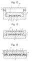
- Fig. 12 shows a conventional art described in Japanese Patent Application Publication No. 2001-53577 (hereinafter simply referred to as Document 1) or Japanese Patent Application Publication No. 2001-110946 (Document 2).
- Fig. 12 shows a typical structure of an electronic device fabricated by flip-chip bonding.
- the electronic device has such a basic structure that bumps 2 are provided on a device chip 1 by using metal wires, and the device chip 1 with the bumps 2 is mounted on a wiring pattern 4 provided on a main surface of a ceramic package substrate 3 by a flip-chip bonder.
- the bumps 2 are bonded to the wiring pattern 4. This bonding makes mechanical and electrical connections between the device chip 1 and the package substrate 3.
- a metal lid 10 is used to hermetically seal the device chip 1 in the final step of fabricating the electronic device.
- a seal solder layer 5 and a package-side seal pattern 6 are interposed between the package substrate 3 and the lid 10.
- the device 10 has a hollow portion 8, and an electrode pattern 9.
- Fig. 13 shows another conventional art described in International Publication WO97/02596 (Document 3).
- the device chip 1 and the package substrate 3 are mechanically and electrically connected together in the same manner as that used for the device 10 shown in Fig. 12.
- seal resin 11 is used to establish sealing and form an external shape so that the electronic device is completed.
- Fig. 14 shows yet another conventional art described in Japanese Patent Application Publication No. 2004-129193 (Document 4).
- the device chip 1 and the package substrate 3 are mechanically and electrically connected together in the same manner as that used for the device shown in Fig. 12.
- the seal solder 5 are formed on the main surface of the package substrate 3 beforehand, and sealing is simultaneously performed.
- the seal resin 11 is used to form the outer shape of the electronic device so that the electronic device is completed.
- the device shown in Fig. 12 employs the metal lid 10 and the seal solder 5 to realize high hermetic seal and strong outer shape.
- the package substrate is required to have sidewalls, which prevents downsizing, reduced height and cost reduction of the device.
- the device shown in Fig. 13 employs the seal resin 11, which may contribute to downsizing and height reduction.
- the device does not have good hermetic seal and comparatively low reliability.
- the device may be liable to be affected by external waves because the entire chip is not shielded by metal. Particularly, poor shield may cause degraded performance of high-frequency (RF) components.
- RF high-frequency
- the device shown in Fig. 14 may overcome the drawbacks of the conventional devices shown in Figs. 12 and 13 and is characterized in that the chip is sealed with the seal solder layer 5, and is then sealed with the resin 11.
- the device uses the two different materials for sealing and forming the outer shape, and has a problem in terms of the cost. It is also required to form the seal solder layer on the package substrate beforehand. This may produce devices having errors in shape and limit the time for thermal treatment.
- Mass productivity may be improved by flip-chip mounting chips on a sheet-shaped multi-production substrate and by simultaneously performing soldering. In this process, the whole sheet-shaped substrate is inevitably heated up to 300 °C or higher for a couple of minutes. This thermal treatment causes the metal layer mounted on the device chip and the package substrate and adapt to solder to be melted in solder, and degrades the reliability.
- the present invention has been made in view of the above circumstances and provides a compact, height-reduced, less-expensive and reliable electronic device and a method of fabricating the same.
- an electronic device including: a package substrate made of an insulator; a device chip that is flip-chip mounted on the package substrate; and a seal portion sealing the device chip, the seal portion being sidewalls made of solder.
- a method of fabricating an electronic device comprising the steps of: flip-chip mounting a device chip on a package substrate; and supplying solder to at least one of the package substrate and the device chip and heating the solder to be melted so that a seal portion made of solder is formed on the package substrate.
- a method of fabricating an electronic device comprising the steps of: flip-chip mounting device chips on a package substrate; and supplying solder to at least one of the package substrate and the device chips and heating the solder to be melted so that a seal portion made of solder is formed on the package substrate so as to cover the device chips.
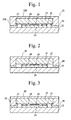
- Fig. 1 is a cross-sectional view of an electronic device in accordance with a first embodiment of the present invention.
- the device has a device chip 21 and a package substrate 23, which are electrically and mechanically connected by bumps 22 made of Au or an alloy including Au.
- the device chip 21 has desired electrical characteristics.
- the package substrate 23 is made of an insulator such as resin or ceramics.
- a wiring pattern 24 is formed on an upper surface of the package 23.
- the device chip 21 is flip-chip mounted on the wiring pattern 24 through the bumps 22 in the facedown state.
- the device chip has an electrode pattern 29, which may be an interdigital transducer (comb-like electrodes) of a surface acoustic wave device.
- the device chip 21 has not-shown pads, on which the bumps 22 are provided.
- the device chip 21 and the package substrate 23 are sealed with a seal portion 25 made of solder.
- the solder seal portion 25 covers the whole chip, and defines an outer shape of the electronic device.
- the solder seal portion 25 forms the package of the electronic device along with the package substrate 23.
- the solder seal portion 25 forms side portions 25A and an upper portion 25B.
- the side and upper surfaces of the package are formed by solder of the solder seal portion 25.
- the solder seal portion 25 forms a cavity (hollow portion) 28 within the package.
- the device chip 21 is hermetically sealed within the cavity 28.
- the peripheral portions of the device chip 21 and those of the package substrate 23 are respectively provided with a chip-side seal pattern 27 and a package-side seal pattern 26, which patterns are made of metal and are provided in corresponding positions.
- the chip-side seal pattern 27 overlaps with a part of the package-side seal pattern 26.
- the seal patterns 26 and 27 function as areas for facilitating flow of solder for forming the solder seal portion 25.
- an end portion of the solder seal portion 25 is bonded to the package-side seal pattern 26 and the chip-side seal pattern 27, and slightly protrudes to the cavity 28.
- the package-side seal pattern 26 and the chip-side seal pattern 27 are made of a metal having a good wettability to solder.
- the seal patterns 26 and 27 may be a single layer of metal or may be compose of multiple layers made of different metals.
- the patterns 26 and 27 may have a two-layer structure composed of a Ni layer and an Au layer.
- the first embodiment of the present invention seals the whole device chip 21 with the solder seal portion 25 joined to the package substrate 23.
- the electronic device thus configured has high airtightness, excellent electrical shielding, reliable bonding, a substantial outer shape, and a reduced height.
- the present electronic device may be fabricated by a simple process, and is thus less expensive.
- the solder seal portion 25 may be made of Sn-Ag solder. Another arbitrary solder may be used as the solder seal portion 25.
- Fig. 2 is a cross-sectional view of an electronic device in accordance with a second embodiment of the present invention, in which parts that are the same as those shown in Fig. 1 are given the same reference numerals as previously.
- the solder seal portion 25 seals the whole device chip 21 as the solder seal portion 25 shown in Fig. 1.
- the structure shown in Fig. 2 does not have the chip-side seal pattern 27 shown in Fig. 1 and a shape such that the outer size of the device chip 21 is substantially equal to the inside dimension of the package-side seal pattern 26. This prevents the fluidized seal solder 25 from flowing along the backside of the device chip 21 and forms the shape shown in Fig. 2 having the sealed hollow region.
- the whole device chip 21 is sealed by the solder seal portion 25 bonded to the package substrate 23.
- the electronic device thus configured has high airtightness, excellent electrical shielding, reliable bonding, a substantial outer shape and a reduced height.
- Fig. 3 is a cross-sectional view of an electronic device in accordance with a third embodiment of the present invention, in which parts that are the same as those shown in Fig. 1 are given the same reference numerals as previously.
- the electronic device of the third embodiment has a structure in which a metal layer 32 is provided on the solder seal portion 25 provided along the peripheral portions of the device chip 21. That is, the combination of the solder seal portion 25 and the metal layer 32 defines the seal portion on the package substrate 23.
- the metal layer 32 may be made of a kovar alloy. The metal layer 32 functions to protect the entire electronic device and an auxiliary structural member for solder.
- the kovar alloy has a thermal expansion coefficient close to that of ceramics, and thus functions to absorb the difference in thermal expansion coefficient between a piezoelectric substrate such as a SAW chip and ceramics of the package substrate 23. It is therefore possible to prevent considerable stress from being applied to the SAW chip of the completed electronic device and greatly improve the reliability and electrical performance.
- the third embodiment has the same advantages as those of the first embodiment.
- Fig. 4 is a cross-sectional view of an electronic device in accordance with a fourth embodiment of the present invention, in which parts that are the same as those shown in Fig. 1 are given the same reference numerals as previously.
- the electronic device of the fourth embodiment has a structure in which a resin layer 33 is provided on the solder seal portion 25 provided on the peripheral portions of the device chip 21.
- the combination of the solder seal portion 25 and the resin layer 33 defines the seal region on the package substrate 23.
- the resin layer 33 may be a sheet-like polyamide layer (having a Cu wiring pattern on an either side thereof). This film for the resin layer 33 may be substituted for a glass-epoxy film layer.
- Figs. 5A through 5C show a process of fabricating an electronic device in accordance with a fifth embodiment of the present invention. More specifically, the fifth embodiment is the method of fabricating the electronic devices that have the structure of the first or second embodiment.
- the fifth embodiment is the method of fabricating the electronic devices that have the structure of the first or second embodiment.
- multiple device chips 21 are mounted on a multiple package substrate 140 in rows and columns, and are flip-chip bonded thereto.
- a Sn-Ag solder sheet 150 is positioned on the device chips 21.
- the solder sheet 150 is heated and pressurized from the upper side of the solder sheet 150. This process may be performed at a temperature necessary to melt solder and under a pressure necessary to form the outer shape of the package.
- solder portions interposed between the device chips 21 bond the package-side seal patterns 26 and the not-shown chip-side seal patterns 27 (for the first embodiment) together.
- This bonding may be performed in a nitrogen atmosphere at a temperature of approximately 270 °C.
- the package substrate 140 is cut into the individual pieces by a dicer or the like, so that multiple electronic devices are available.
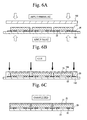
- Figs. 6A through 6C show a process of fabricating an electronic device in accordance with a sixth embodiment of the present invention.
- This process fabricates the electronic devices of the first or second embodiment.
- the present process differs from the fifth embodiment in that the package substrate 140 is heated from the backside thereof beforehand, and the sheet 150 is placed on the device chips 21 with a pressure being applied thereto from the upper sides thereof.
- the steps of Figs. 6B and 6C are similar to those of Figs. 5B and 5C.
- the electronic device of the second embodiment may be fabricated in the same manner as shown in Figs. 6A through 6C.
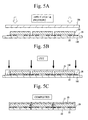
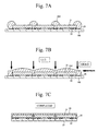
- Figs. 7A through 7C show a process of fabricating an electronic device in accordance with a seventh embodiment of the present invention. This process fabricates the electronic devices of the first or second embodiment. As shown in Fig. 7A, solder paste members 250 are provided in the gaps defined by the neighboring device chips 21, and are reflown. Next, as shown in Fig. 7B, the solder paste members 250 are grinded, and the package substrate 140 is cut into pieces by the dicer. Thus, multiple electronic devices of the first embodiment are available, as shown in Fig. 7C.
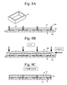
- Figs. 8A through 8C show a process of fabricating an electronic device in accordance with an eight embodiment of the present invention. This process fabricates the electronic devices of the first or second embodiment.
- washers 350 are provided so that each of the device chips 21 on the package substrate 140 is inserted into the respective washers 350.
- the washers are made of solder and are formed into a frame.
- the washers 350 may be applied to some of the devices chips 21.
- the washers 350 may be alternately applied to the device chips 21 in an X or Y direction or both the directions.
- the subsequent steps of Figs. 8B and 8C are the same as those of Figs. 7B and 7C.
- the washers 350 may be substituted for a solder sheet having openings arranged in rows and columns.
- the device chips 21 are inserted into the openings of the solder sheet, which is then reflown.
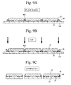
- Figs. 9A through 9C show a process of fabricating an electronic device in accordance with a ninth embodiment of the present invention.
- the present embodiment employs solder balls 450 for the solder paste members 250 used in the seventh embodiment.
- the solder balls 450 are placed in the gaps defined by the neighboring device chips 21 and are then reflown.
- the package substrate 140 after reflow is shown in Fig. 9B.
- the package substrate 140 is cut into the pieces by the dicer.
- Fig. 9C multiple electronic devices are available in which the device chips 21 are sealed with packages having side portions 45 made of solder.
- the present device chips do not have any solder package provided on the device chips 21.
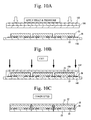
- Figs. 10A through 10C show a process of fabricating an electronic device in accordance with a tenth embodiment of the present invention.
- the present process fabricates the electronic devices of the third embodiment.
- a metal layer 132 is placed on the solder sheet 150, and the laminate thus formed is placed on the device chips 21 on a package substrate 140.
- the laminate is heated and pressurized from the upper side of the metal layer 132. This process may be performed at a temperature necessary to melt solder and under a pressure necessary to form the outer shape of the package.
- the solders that enter into the gaps between the neighboring device chips 21 bond the package-side seal patterns 26 and the not-shown chip-side seal patterns 27 (for the first embodiment).
- the metal layer 132 are provided above the device chips 21 on the package substrate 140 via the solder layer, and the side and upper surfaces of the device chips 21 are covered with solder.
- the package substrate 140 thus formed is cut into pieces by the dicer, so that multiple electronic devices of the third embodiment can be produced, as shown in Fig. 10C.
- the package substrate 140 may be heated beforehand, as shown in Fig. 6A.
- Figs. 11A through 11C shows a process of fabricating an electronic device in accordance with an eleventh embodiment of the present invention.
- the present process fabricates the electronic devices of the fourth embodiment.
- a resin layer 133 which may be a polyamide layer, is placed on the solder sheet 150, and the laminate thus formed is placed on the device chips 21.
- the laminate is heated and pressurized from the upper side of the resin layer 133. This process may be performed at a temperature necessary to melt solder and under a pressure necessary to form the outer shape of the package.
- the solders that enter into the gaps between the neighboring device chips 21 bond the package-side seal patterns 26 and the not-shown chip-side seal patterns 27 (for the first embodiment).
- the resin layer 133 are provided above the device chips 21 on the package substrate 140 via the solder layer, and the side and upper surfaces of the device chips 21 are covered with solder.
- the package substrate 140 thus formed is cut into pieces by the dicer, so that multiple electronic devices of the fourth embodiment can be produced, as shown in Fig. 11C.
- the package substrate 140 may be heated beforehand, as shown in Fig. 6A.
- a twelfth embodiment of the present invention has a structure in which a protection film is provided to the electronic devices of the first through fourth embodiments of the present invention.
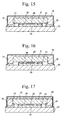
- Fig. 15 is a cross-sectional view of an electronic device having a protection film 34 provided to the electronic device of the first embodiment.
- the protection film 34 covers the whole surface of the seal portion 25 and covers the package-side seal pattern 26 and the surface of the package substrate 23. That is, the protection film 34 hermetically seals the cavity 28.
- the protection film 34 may be a metal film or a resin film (insulation film).
- Ni is deposited to a thickness of 10 to 20 ⁇ m by electrolytic plating to thus form the protection film 34.
- a plating film of Cu or a vapor deposition film may be used as the protection film 34.
- the protection film 34 prevents the solder seal portion 25 inside the protection film 34 from being deformed due to external force or heat, and improves the heat-resistant temperature of the electronic device. Ni plating totally covers the solder portions, and prevent the performance and external appearance of the electronic device from being damaged even when the electronic device has a reflow profile over the melting point of solder.
- the resin used for the protection film 34 may, for example, be epoxy resin. Epoxy resin may be deposited by spray to form the protection film 34.
- Fig. 16 is a cross-sectional view of an electronic device in which the protection film 34 is applied to the second embodiment shown in Fig. 2.
- the structure and function of the protection film 34 shown in Fig. 16 are the same as those of the protection film 34 shown in Fig. 15.
- Fig. 17 is a cross-sectional view of an electronic device in which the protection film 34 is applied to the third embodiment shown in Fig. 3.
- the protection film 34 is provided so as to cover the solder seal portion 25, the metal layer 32, the package-side seal pattern 26 and the package substrate 23.
- the structure and function of the protection pattern shown in Fig. 17 are the same as those of the protection pattern shown in Fig. 15.
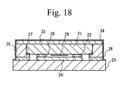
- Fig. 18 is a cross-sectional view of an electronic device in which the protection film 34 is applied to the fourth embodiment shown in Fig. 4.
- the protection film 34 is provided so as to cover the solder seal portion 25, the resin layer 33, the package-side seal pattern 26 and the package substrate 23.
- the structure and function of the protection pattern shown in Fig. 18 are the same as those of the protection pattern 34 shown in Fig. 15.
- Figs. 19A through 19D show a process of fabricating the electronic device shown in Fig. 17.
- the steps of Figs. 19A and 19B are the same as those shown in Figs. 5A and 5B, respectively.
- Fig. 19C grooves 19 are formed in the solder portions interposed between the adjacent device chips 21.
- the protection film 34 is formed.
- Fig. 19D the package substrate 140 is cut into pieces in the same manner as that shown in Fig. 5C. In this manner, multiple electronic devices shown in Fig. 17 are all available at once.
- the grooves 39 may be provided to electronic devices shown in Figs. 15 and 16.
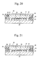
- Fig. 20 is a cross-sectional view of an electronic device in accordance with a thirteenth embodiment of the present invention.
- the present electronic device is a variation of the electronic device shown in Fig. 3.
- metal balls 35 coexist in the solder seal portion 25.
- the metal balls 35 are buried in the sidewalls of the solder seal portion 25.
- the solder seal portion 25 defines the sidewalls of the package, and the metal balls 35 are covered with solder of the solder seal portion 25.
- the metal balls 35 may be Cu balls having a diameter of 0.15 mm.
- the surfaces of the Cu balls are plated with Sn.
- the solder seal portion 25 may be made of Sn-Ag.
- a Sn-Cu based compound is produced to form a high-melting-point layer.
- the heat-resistant characteristic obtained when the metal balls 35 are used is superior to that obtained in the absence of the metal balls 35. It has been confirmed that Ni balls bring about the same functions and effects as those of Cu balls.
- the use of the metal balls 35 additionally brings about reduction in the volume of solder. This contributes to cost reduction, particularly when expensive solder such as Au-Sn solder is used for the solder seal portion 25.
- Fig. 21 is a cross-sectional view of an electronic device in which a metal frame 36 is substituted for the metal balls 35.
- the metal frame 36 is covered with solder of the solder seal portion 25.
- the metal frame 36 is buried in the sidewalls of the solder seal portion 25.
- the metal frame 36 is positioned on the package-side seal pattern 26.
- the metal frame 36 is formed so as to surround the device chip 21.
- the metal frame 36 may be made of a material having good wettability to solder, such as kovar.
- a material having a poor wettability to solder may be applied to the metal frame 36. In this case, the material may be subjected to surface treatment.
- the metal frame 36 brings about the functions and effects similar to those of the metal balls 35.
- the metal balls 35 and the metal frame 36 is not limited to the structure shown in Fig. 3 but may be applied to the electronic devices shown in Figs. 1, 2 and 4 and those shown in Figs. 15 through 18.
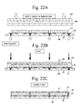
- Figs. 22A through 22C show a process of fabricating the electronic device shown in Fig. 21.
- through holes 37 are formed in the multiple package substrate 140.
- a single or multiple through holes 37 may be formed between the neighboring device chips 21.
- the through holes 37 function to facilitate discharging of surplus air to the outside of the device when the solder sheet 150 supplied from the upper surfaces of the device chips 21 together with the metal layer 132 are heated and pressurized.
- the package substrate 140 is cut into pieces by the dicer, so that multiple electronic devices are all available at once, as shown in Fig. 22C. It has been confirmed that the through holes 37 greatly improve the yield of the electronic devices having an outside dimension of 1.4 mm x 1.0 mm.
- the present invention is based on Japanese Patent Application No. 2004-374596 filed December 24, 2004 and Japanese Patent Application No. 2005-056722 filed March 1, 2005, the entire disclosure of which is hereby incorporated by reference.
Landscapes
- Physics & Mathematics (AREA)
- Acoustics & Sound (AREA)
- Wire Bonding (AREA)
- Surface Acoustic Wave Elements And Circuit Networks Thereof (AREA)
- Structures Or Materials For Encapsulating Or Coating Semiconductor Devices Or Solid State Devices (AREA)
Abstract
Description
- The present invention relates to an electronic device and a method of fabricating the same, and more particularly, to the technique of packaging a device chip on a package substrate in flip-chip mounting.
- Conventionally, wire bonding is used to make mechanical and electrical connections between a chip of an electronic device and a package. In wire bonding, the device chip is mechanically connected to the package by an adhesive, and is electrically connected thereto by metal wires. Recently, the mainstream connection method is flip-chip bonding in which bumps are used to connect the chip and the package.
- Fig. 12 shows a conventional art described in Japanese Patent Application Publication No. 2001-53577 (hereinafter simply referred to as Document 1) or Japanese Patent Application Publication No. 2001-110946 (Document 2). Fig. 12 shows a typical structure of an electronic device fabricated by flip-chip bonding. The electronic device has such a basic structure that
bumps 2 are provided on adevice chip 1 by using metal wires, and thedevice chip 1 with thebumps 2 is mounted on awiring pattern 4 provided on a main surface of aceramic package substrate 3 by a flip-chip bonder. Thebumps 2 are bonded to thewiring pattern 4. This bonding makes mechanical and electrical connections between thedevice chip 1 and thepackage substrate 3. Then, ametal lid 10 is used to hermetically seal thedevice chip 1 in the final step of fabricating the electronic device. Aseal solder layer 5 and a package-side seal pattern 6 are interposed between thepackage substrate 3 and thelid 10. Thedevice 10 has ahollow portion 8, and anelectrode pattern 9. - Fig. 13 shows another conventional art described in International Publication WO97/02596 (Document 3). The
device chip 1 and thepackage substrate 3 are mechanically and electrically connected together in the same manner as that used for thedevice 10 shown in Fig. 12. Then,seal resin 11 is used to establish sealing and form an external shape so that the electronic device is completed. - Fig. 14 shows yet another conventional art described in Japanese Patent Application Publication No. 2004-129193 (Document 4). The
device chip 1 and thepackage substrate 3 are mechanically and electrically connected together in the same manner as that used for the device shown in Fig. 12. During the process, theseal solder 5 are formed on the main surface of thepackage substrate 3 beforehand, and sealing is simultaneously performed. Then, theseal resin 11 is used to form the outer shape of the electronic device so that the electronic device is completed. - The conventional arts mentioned above that use flip-chip bonding to connect the device chip and the package substrate have a possibility that a foreign object may contact the
electrode pattern 9 formed on the chip surface or moisture may enter into the contact so that the device does not function. Particularly, the above problem is serious to acoustic filters that use an elastic wave, such as surface acoustic wave (SAW) devices and film bulk acoustic resonators (FBARs). It is thus essential to hermetically seal the hollow region to protect theelectrode pattern 9 from outside air. - However, the conventional arts have the respective drawbacks mentioned below. The device shown in Fig. 12 employs the
metal lid 10 and theseal solder 5 to realize high hermetic seal and strong outer shape. However, the package substrate is required to have sidewalls, which prevents downsizing, reduced height and cost reduction of the device. - The device shown in Fig. 13 employs the
seal resin 11, which may contribute to downsizing and height reduction. However, the device does not have good hermetic seal and comparatively low reliability. Further, the device may be liable to be affected by external waves because the entire chip is not shielded by metal. Particularly, poor shield may cause degraded performance of high-frequency (RF) components. - The device shown in Fig. 14 may overcome the drawbacks of the conventional devices shown in Figs. 12 and 13 and is characterized in that the chip is sealed with the
seal solder layer 5, and is then sealed with theresin 11. However, the device uses the two different materials for sealing and forming the outer shape, and has a problem in terms of the cost. It is also required to form the seal solder layer on the package substrate beforehand. This may produce devices having errors in shape and limit the time for thermal treatment. Mass productivity may be improved by flip-chip mounting chips on a sheet-shaped multi-production substrate and by simultaneously performing soldering. In this process, the whole sheet-shaped substrate is inevitably heated up to 300 °C or higher for a couple of minutes. This thermal treatment causes the metal layer mounted on the device chip and the package substrate and adapt to solder to be melted in solder, and degrades the reliability. - The present invention has been made in view of the above circumstances and provides a compact, height-reduced, less-expensive and reliable electronic device and a method of fabricating the same.
- According to an aspect of the present invention, there is provided an electronic device including: a package substrate made of an insulator; a device chip that is flip-chip mounted on the package substrate; and a seal portion sealing the device chip, the seal portion being sidewalls made of solder.
- According to another aspect of the present invention, there is provided a method of fabricating an electronic device comprising the steps of: flip-chip mounting a device chip on a package substrate; and supplying solder to at least one of the package substrate and the device chip and heating the solder to be melted so that a seal portion made of solder is formed on the package substrate.
- According to a further aspect of the present invention, there is provided a method of fabricating an electronic device comprising the steps of: flip-chip mounting device chips on a package substrate; and supplying solder to at least one of the package substrate and the device chips and heating the solder to be melted so that a seal portion made of solder is formed on the package substrate so as to cover the device chips.
- Other objects, features and advantages of the present invention will become more apparent from the following detailed description when read in conjunction with the accompanying drawings, in which:
- Fig. 1 is a cross-sectional view of an electronic device in accordance with a first embodiment of the present invention;
- Fig. 2 is a cross-sectional view of an electronic device in accordance with a second embodiment of the present invention;
- Fig. 3 is a cross-sectional view of an electronic device in accordance with a third embodiment of the present invention;
- Fig. 4 is a cross-sectional view of an electronic device in accordance with a fourth embodiment of the present invention;
- Figs. 5A through 5C show a method of fabricating an electronic device in accordance with a fifth embodiment of the present invention;
- Figs. 6A through 6C show a method of fabricating an electronic device in accordance with a sixth embodiment of the present invention;
- Figs. 7A through 7C show a method of fabricating an electronic device in accordance with a seventh embodiment of the present invention;
- Figs. 8A through 8C show a method of fabricating an electronic device in accordance with an eighth embodiment of the present invention;
- Figs. 9A through 9C show a method of fabricating an electronic device in accordance with a ninth embodiment of the present invention;
- Figs. 10A through 10C show a method of fabricating an electronic device in accordance with a tenth embodiment of the present invention;
- Figs 11A through 11C show a method of fabricating an electronic device in accordance with an eleventh embodiment of the present invention;
- Fig. 12 is a cross-sectional view of a conventional electronic device;
- Fig. 13 is a cross-sectional view of another conventional electronic device;
- Fig. 14 is a cross-sectional view of yet another conventional electronic device;
- Fig. 15 is a cross-sectional view of an electronic device in accordance with a twelfth embodiment of the present invention, which is a variation of the electronic device in accordance with the first embodiment;
- Fig. 16 is a cross-sectional view of another electronic device in accordance with the twelfth embodiment of the present invention, which is a variation of the electronic device in accordance with the second embodiment;
- Fig. 17 is a cross-sectional view of yet another electronic device in accordance with the twelfth embodiment of the present invention, which is a variation of the electronic device in accordance with the third embodiment;
- Fig. 18 is a cross-sectional view of a further electronic device in accordance with the twelfth embodiment of the present invention, which is a variation of the electronic device in accordance with the fourth embodiment;
- Figs. 19A through 19D show a method of fabricating the electronic device shown in Fig. 17;
- Fig. 20 is a cross-sectional view of an electronic device in accordance with a thirteenth embodiment of the present invention;
- Fig. 21 is a cross-sectional view of a variation of the electronic device in accordance with the thirteenth embodiment of the present invention; and
- Figs. 22A through 22C show a process of fabricating the electronic device shown in Fig. 21.
- A description will now be given, with reference to the accompanying drawings, of preferred embodiments of the present invention.
- Fig. 1 is a cross-sectional view of an electronic device in accordance with a first embodiment of the present invention. The device has a
device chip 21 and apackage substrate 23, which are electrically and mechanically connected bybumps 22 made of Au or an alloy including Au. Thedevice chip 21 has desired electrical characteristics. Thepackage substrate 23 is made of an insulator such as resin or ceramics. Awiring pattern 24 is formed on an upper surface of thepackage 23. Thedevice chip 21 is flip-chip mounted on thewiring pattern 24 through thebumps 22 in the facedown state. The device chip has anelectrode pattern 29, which may be an interdigital transducer (comb-like electrodes) of a surface acoustic wave device. Thedevice chip 21 has not-shown pads, on which thebumps 22 are provided. Thedevice chip 21 and thepackage substrate 23 are sealed with aseal portion 25 made of solder. Thesolder seal portion 25 covers the whole chip, and defines an outer shape of the electronic device. Thesolder seal portion 25 forms the package of the electronic device along with thepackage substrate 23. Thesolder seal portion 25forms side portions 25A and anupper portion 25B. The side and upper surfaces of the package are formed by solder of thesolder seal portion 25. Thesolder seal portion 25 forms a cavity (hollow portion) 28 within the package. Thedevice chip 21 is hermetically sealed within thecavity 28. The peripheral portions of thedevice chip 21 and those of thepackage substrate 23 are respectively provided with a chip-side seal pattern 27 and a package-side seal pattern 26, which patterns are made of metal and are provided in corresponding positions. The chip-side seal pattern 27 overlaps with a part of the package-side seal pattern 26. In the fabrication process, theseal patterns solder seal portion 25. Thus, an end portion of thesolder seal portion 25 is bonded to the package-side seal pattern 26 and the chip-side seal pattern 27, and slightly protrudes to thecavity 28. The package-side seal pattern 26 and the chip-side seal pattern 27 are made of a metal having a good wettability to solder. Theseal patterns patterns - As described above, the first embodiment of the present invention seals the
whole device chip 21 with thesolder seal portion 25 joined to thepackage substrate 23. The electronic device thus configured has high airtightness, excellent electrical shielding, reliable bonding, a substantial outer shape, and a reduced height. As will be described later, the present electronic device may be fabricated by a simple process, and is thus less expensive. - The
solder seal portion 25 may be made of Sn-Ag solder. Another arbitrary solder may be used as thesolder seal portion 25. - Fig. 2 is a cross-sectional view of an electronic device in accordance with a second embodiment of the present invention, in which parts that are the same as those shown in Fig. 1 are given the same reference numerals as previously. The
solder seal portion 25 seals thewhole device chip 21 as thesolder seal portion 25 shown in Fig. 1. The structure shown in Fig. 2 does not have the chip-side seal pattern 27 shown in Fig. 1 and a shape such that the outer size of thedevice chip 21 is substantially equal to the inside dimension of the package-side seal pattern 26. This prevents thefluidized seal solder 25 from flowing along the backside of thedevice chip 21 and forms the shape shown in Fig. 2 having the sealed hollow region. In the second embodiment, thewhole device chip 21 is sealed by thesolder seal portion 25 bonded to thepackage substrate 23. The electronic device thus configured has high airtightness, excellent electrical shielding, reliable bonding, a substantial outer shape and a reduced height. - Fig. 3 is a cross-sectional view of an electronic device in accordance with a third embodiment of the present invention, in which parts that are the same as those shown in Fig. 1 are given the same reference numerals as previously. The electronic device of the third embodiment has a structure in which a
metal layer 32 is provided on thesolder seal portion 25 provided along the peripheral portions of thedevice chip 21. That is, the combination of thesolder seal portion 25 and themetal layer 32 defines the seal portion on thepackage substrate 23. Themetal layer 32 may be made of a kovar alloy. Themetal layer 32 functions to protect the entire electronic device and an auxiliary structural member for solder. The kovar alloy has a thermal expansion coefficient close to that of ceramics, and thus functions to absorb the difference in thermal expansion coefficient between a piezoelectric substrate such as a SAW chip and ceramics of thepackage substrate 23. It is therefore possible to prevent considerable stress from being applied to the SAW chip of the completed electronic device and greatly improve the reliability and electrical performance. Of course, the third embodiment has the same advantages as those of the first embodiment. - Fig. 4 is a cross-sectional view of an electronic device in accordance with a fourth embodiment of the present invention, in which parts that are the same as those shown in Fig. 1 are given the same reference numerals as previously. The electronic device of the fourth embodiment has a structure in which a
resin layer 33 is provided on thesolder seal portion 25 provided on the peripheral portions of thedevice chip 21. The combination of thesolder seal portion 25 and theresin layer 33 defines the seal region on thepackage substrate 23. Theresin layer 33 may be a sheet-like polyamide layer (having a Cu wiring pattern on an either side thereof). This film for theresin layer 33 may be substituted for a glass-epoxy film layer. - Figs. 5A through 5C show a process of fabricating an electronic device in accordance with a fifth embodiment of the present invention. More specifically, the fifth embodiment is the method of fabricating the electronic devices that have the structure of the first or second embodiment. Referring to Fig. 5A,
multiple device chips 21 are mounted on amultiple package substrate 140 in rows and columns, and are flip-chip bonded thereto. Next, a Sn-Ag solder sheet 150 is positioned on the device chips 21. Then, thesolder sheet 150 is heated and pressurized from the upper side of thesolder sheet 150. This process may be performed at a temperature necessary to melt solder and under a pressure necessary to form the outer shape of the package. The solder portions interposed between the device chips 21 bond the package-side seal patterns 26 and the not-shown chip-side seal patterns 27 (for the first embodiment) together. This bonding may be performed in a nitrogen atmosphere at a temperature of approximately 270 °C. This results in thepackage substrate 140 on which the side and upper surfaces of the device chips 21 are covered with solder, as shown in Fig. 5B. Finally, thepackage substrate 140 is cut into the individual pieces by a dicer or the like, so that multiple electronic devices are available. - Figs. 6A through 6C show a process of fabricating an electronic device in accordance with a sixth embodiment of the present invention. This process fabricates the electronic devices of the first or second embodiment. The present process differs from the fifth embodiment in that the
package substrate 140 is heated from the backside thereof beforehand, and thesheet 150 is placed on the device chips 21 with a pressure being applied thereto from the upper sides thereof. The steps of Figs. 6B and 6C are similar to those of Figs. 5B and 5C. The electronic device of the second embodiment may be fabricated in the same manner as shown in Figs. 6A through 6C. - Figs. 7A through 7C show a process of fabricating an electronic device in accordance with a seventh embodiment of the present invention. This process fabricates the electronic devices of the first or second embodiment. As shown in Fig. 7A,
solder paste members 250 are provided in the gaps defined by the neighboring device chips 21, and are reflown. Next, as shown in Fig. 7B, thesolder paste members 250 are grinded, and thepackage substrate 140 is cut into pieces by the dicer. Thus, multiple electronic devices of the first embodiment are available, as shown in Fig. 7C. - Figs. 8A through 8C show a process of fabricating an electronic device in accordance with an eight embodiment of the present invention. This process fabricates the electronic devices of the first or second embodiment. As shown in Fig. 8A,
washers 350 are provided so that each of the device chips 21 on thepackage substrate 140 is inserted into therespective washers 350. The washers are made of solder and are formed into a frame. Thewashers 350 may be applied to some of the devices chips 21. For example, thewashers 350 may be alternately applied to the device chips 21 in an X or Y direction or both the directions. The subsequent steps of Figs. 8B and 8C are the same as those of Figs. 7B and 7C. Thewashers 350 may be substituted for a solder sheet having openings arranged in rows and columns. The device chips 21 are inserted into the openings of the solder sheet, which is then reflown. - Figs. 9A through 9C show a process of fabricating an electronic device in accordance with a ninth embodiment of the present invention. As shown in Fig. 9A, the present embodiment employs
solder balls 450 for thesolder paste members 250 used in the seventh embodiment. Thesolder balls 450 are placed in the gaps defined by the neighboring device chips 21 and are then reflown. Thepackage substrate 140 after reflow is shown in Fig. 9B. Thepackage substrate 140 is cut into the pieces by the dicer. Thus, as shown in Fig. 9C, multiple electronic devices are available in which the device chips 21 are sealed with packages havingside portions 45 made of solder. The present device chips do not have any solder package provided on the device chips 21. - Figs. 10A through 10C show a process of fabricating an electronic device in accordance with a tenth embodiment of the present invention. The present process fabricates the electronic devices of the third embodiment. Referring to Fig. 10A, a
metal layer 132 is placed on thesolder sheet 150, and the laminate thus formed is placed on the device chips 21 on apackage substrate 140. Next, the laminate is heated and pressurized from the upper side of themetal layer 132. This process may be performed at a temperature necessary to melt solder and under a pressure necessary to form the outer shape of the package. The solders that enter into the gaps between the neighboring device chips 21 bond the package-side seal patterns 26 and the not-shown chip-side seal patterns 27 (for the first embodiment). Thus, as shown in Fig. 10B, themetal layer 132 are provided above the device chips 21 on thepackage substrate 140 via the solder layer, and the side and upper surfaces of the device chips 21 are covered with solder. Thepackage substrate 140 thus formed is cut into pieces by the dicer, so that multiple electronic devices of the third embodiment can be produced, as shown in Fig. 10C. In the step of Fig. 10A, thepackage substrate 140 may be heated beforehand, as shown in Fig. 6A. - Figs. 11A through 11C shows a process of fabricating an electronic device in accordance with an eleventh embodiment of the present invention. The present process fabricates the electronic devices of the fourth embodiment. Referring to Fig. 11A, a
resin layer 133, which may be a polyamide layer, is placed on thesolder sheet 150, and the laminate thus formed is placed on the device chips 21. The laminate is heated and pressurized from the upper side of theresin layer 133. This process may be performed at a temperature necessary to melt solder and under a pressure necessary to form the outer shape of the package. The solders that enter into the gaps between the neighboring device chips 21 bond the package-side seal patterns 26 and the not-shown chip-side seal patterns 27 (for the first embodiment). Thus, as shown in Fig. 11B, theresin layer 133 are provided above the device chips 21 on thepackage substrate 140 via the solder layer, and the side and upper surfaces of the device chips 21 are covered with solder. Thepackage substrate 140 thus formed is cut into pieces by the dicer, so that multiple electronic devices of the fourth embodiment can be produced, as shown in Fig. 11C. In the step of Fig. 11A, thepackage substrate 140 may be heated beforehand, as shown in Fig. 6A. - A twelfth embodiment of the present invention has a structure in which a protection film is provided to the electronic devices of the first through fourth embodiments of the present invention.
- Fig. 15 is a cross-sectional view of an electronic device having a
protection film 34 provided to the electronic device of the first embodiment. Theprotection film 34 covers the whole surface of theseal portion 25 and covers the package-side seal pattern 26 and the surface of thepackage substrate 23. That is, theprotection film 34 hermetically seals thecavity 28. Theprotection film 34 may be a metal film or a resin film (insulation film). For the metal film, Ni is deposited to a thickness of 10 to 20 µm by electrolytic plating to thus form theprotection film 34. Instead of Ni, a plating film of Cu or a vapor deposition film may be used as theprotection film 34. Theprotection film 34 prevents thesolder seal portion 25 inside theprotection film 34 from being deformed due to external force or heat, and improves the heat-resistant temperature of the electronic device. Ni plating totally covers the solder portions, and prevent the performance and external appearance of the electronic device from being damaged even when the electronic device has a reflow profile over the melting point of solder. The resin used for theprotection film 34 may, for example, be epoxy resin. Epoxy resin may be deposited by spray to form theprotection film 34. - Fig. 16 is a cross-sectional view of an electronic device in which the
protection film 34 is applied to the second embodiment shown in Fig. 2. The structure and function of theprotection film 34 shown in Fig. 16 are the same as those of theprotection film 34 shown in Fig. 15. - Fig. 17 is a cross-sectional view of an electronic device in which the
protection film 34 is applied to the third embodiment shown in Fig. 3. Theprotection film 34 is provided so as to cover thesolder seal portion 25, themetal layer 32, the package-side seal pattern 26 and thepackage substrate 23. The structure and function of the protection pattern shown in Fig. 17 are the same as those of the protection pattern shown in Fig. 15. - Fig. 18 is a cross-sectional view of an electronic device in which the
protection film 34 is applied to the fourth embodiment shown in Fig. 4. Theprotection film 34 is provided so as to cover thesolder seal portion 25, theresin layer 33, the package-side seal pattern 26 and thepackage substrate 23. The structure and function of the protection pattern shown in Fig. 18 are the same as those of theprotection pattern 34 shown in Fig. 15. - Figs. 19A through 19D show a process of fabricating the electronic device shown in Fig. 17. The steps of Figs. 19A and 19B are the same as those shown in Figs. 5A and 5B, respectively. Referring to Fig. 19C, grooves 19 are formed in the solder portions interposed between the adjacent device chips 21. Next, as shown in Fig. 19C, the
protection film 34 is formed. Then, as shown in Fig. 19D, thepackage substrate 140 is cut into pieces in the same manner as that shown in Fig. 5C. In this manner, multiple electronic devices shown in Fig. 17 are all available at once. Besides the electronic device shown in Fig. 17, thegrooves 39 may be provided to electronic devices shown in Figs. 15 and 16. - Fig. 20 is a cross-sectional view of an electronic device in accordance with a thirteenth embodiment of the present invention. The present electronic device is a variation of the electronic device shown in Fig. 3. Referring to Fig. 20,
metal balls 35 coexist in thesolder seal portion 25. Themetal balls 35 are buried in the sidewalls of thesolder seal portion 25. In the structure shown in Fig. 20, thesolder seal portion 25 defines the sidewalls of the package, and themetal balls 35 are covered with solder of thesolder seal portion 25. Themetal balls 35 may be Cu balls having a diameter of 0.15 mm. The surfaces of the Cu balls are plated with Sn. Thesolder seal portion 25 may be made of Sn-Ag. At the interfaces of themetal balls 35, a Sn-Cu based compound is produced to form a high-melting-point layer. The heat-resistant characteristic obtained when themetal balls 35 are used is superior to that obtained in the absence of themetal balls 35. It has been confirmed that Ni balls bring about the same functions and effects as those of Cu balls. The use of themetal balls 35 additionally brings about reduction in the volume of solder. This contributes to cost reduction, particularly when expensive solder such as Au-Sn solder is used for thesolder seal portion 25. - Fig. 21 is a cross-sectional view of an electronic device in which a
metal frame 36 is substituted for themetal balls 35. Themetal frame 36 is covered with solder of thesolder seal portion 25. Themetal frame 36 is buried in the sidewalls of thesolder seal portion 25. Themetal frame 36 is positioned on the package-side seal pattern 26. Themetal frame 36 is formed so as to surround thedevice chip 21. Preferably, themetal frame 36 may be made of a material having good wettability to solder, such as kovar. Alternatively, a material having a poor wettability to solder may be applied to themetal frame 36. In this case, the material may be subjected to surface treatment. Themetal frame 36 brings about the functions and effects similar to those of themetal balls 35. - The
metal balls 35 and themetal frame 36 is not limited to the structure shown in Fig. 3 but may be applied to the electronic devices shown in Figs. 1, 2 and 4 and those shown in Figs. 15 through 18. - Figs. 22A through 22C show a process of fabricating the electronic device shown in Fig. 21. Referring to Fig. 22A, through
holes 37 are formed in themultiple package substrate 140. A single or multiple throughholes 37 may be formed between the neighboring device chips 21. The through holes 37 function to facilitate discharging of surplus air to the outside of the device when thesolder sheet 150 supplied from the upper surfaces of the device chips 21 together with themetal layer 132 are heated and pressurized. Then, as shown in Fig. 22B, thepackage substrate 140 is cut into pieces by the dicer, so that multiple electronic devices are all available at once, as shown in Fig. 22C. It has been confirmed that the throughholes 37 greatly improve the yield of the electronic devices having an outside dimension of 1.4 mm x 1.0 mm. - The present invention is not limited to the specifically disclosed embodiments, but other embodiments and variations may be made without departing from the scope of the present invention.
- The present invention is based on Japanese Patent Application No. 2004-374596 filed December 24, 2004 and Japanese Patent Application No. 2005-056722 filed March 1, 2005, the entire disclosure of which is hereby incorporated by reference.
Claims (23)
- An electronic device comprising:a package substrate made of an insulator;a device chip that is flip-chip mounted on the package substrate; anda seal portion sealing the device chip,the seal portion being sidewalls made of solder.
- The electronic device as claimed in claim 1, wherein the whole seal portion including the sidewalls is made of solder.
- The electronic device as claimed in claim 1, further comprising a metal layer provided on the seal portion.
- The electronic device as claimed in claim 1, further comprising a resin layer provided on the seal portion.
- The electronic device as claimed in claim 1, wherein:the sidewalls of the seal portion define a cavity in which the device chip is mounted.
- The electronic device as claimed in claim 1, further comprising first and second metal patterns respectively provided on a peripheral portion of the package substrate and a peripheral portion of the device chip, wherein:the second metal pattern overlaps with a part of the first metal pattern; andthe sidewalls made of solder contact the first and second metal patterns.
- The electronic device as claimed in claim 1, further comprising a metal pattern on a peripheral portion of the package substrate, the sidewalls made of solder contacting the metal pattern.
- The electronic device as claimed in claim 1, further comprising a protection film that covers the seal portion.
- The electronic device as claimed in claim 1, further comprising a protection film covering the seal portion and a metal or resin layer provided on the seal portion.
- The electronic device as claimed in claim 1, further comprising a protection film that is one of a metal film and a resin film.
- The electronic device as claimed in claim 1, wherein the sidewalls made of solder include metal balls buried therein.
- The electronic device as claimed in claim 1, wherein the sidewalls made of solder include a frame buried therein.
- A method of fabricating an electronic device comprising the steps of:flip-chip mounting a device chip on a package substrate; andsupplying solder to at least one of the package substrate and the device chip and heating the solder to be melted so that a seal portion made of solder is formed on the package substrate.
- The method as claimed in claim 13, wherein the step of supplying solder comprises a step of supplying a solder sheet to the device chip and heating and pressurizing the solder sheet.
- The method as claimed in claim 13, wherein the step of supplying solder comprises steps of:heating the package substrate;supplying a solder sheet to the device chip and pressurizing the solder sheet.
- The method as claimed in claim 13, wherein the step of supplying solder comprises steps of:supplying a solder sheet to the device chip; andreflowing the solder sheet.
- The method as claimed in claim 13, wherein the step of supplying solder comprises steps of:supplying solder paste to the device chip; andreflowing the solder paste.
- The method as claimed in claim 13, wherein the step of supplying solder comprises steps of:supplying solder washers to the device chip; andreflowing the solder washers.
- The method as claimed in claim 13, wherein the step of supplying solder comprises steps of:supplying a solder sheet having openings arranged in rows and columns to device chips so as to be fit into the openings; andreflowing the solder sheet.
- The method as claimed in claim 13, wherein the step of supplying solder comprises steps of:supplying solder balls arranged close to device chips; andreflowing the solder balls.
- A method of fabricating an electronic device comprising the steps of:flip-chip mounting device chips on a package substrate; andsupplying solder to at least one of the package substrate and the device chips and heating the solder to be melted so that a seal portion made of solder is formed on the package substrate so as to cover the device chips.
- The method as claimed in claim 21, further comprising a step of forming through holes in the package substrate in positions along which the package substrate is cut into pieces.
- The method as claimed in claim 21, further comprising steps of:forming grooves in solder portions located between neighboring device chips; andforming a protection film on the seal portion.
Applications Claiming Priority (2)
| Application Number | Priority Date | Filing Date | Title |
|---|---|---|---|
| JP2004374596 | 2004-12-24 | ||
| JP2005056722A JP4456503B2 (en) | 2004-12-24 | 2005-03-01 | Manufacturing method of electronic parts |
Publications (2)
| Publication Number | Publication Date |
|---|---|
| EP1675259A2 true EP1675259A2 (en) | 2006-06-28 |
| EP1675259A3 EP1675259A3 (en) | 2012-05-02 |
Family
ID=36095641
Family Applications (1)
| Application Number | Title | Priority Date | Filing Date |
|---|---|---|---|
| EP05257680A Withdrawn EP1675259A3 (en) | 2004-12-24 | 2005-12-14 | Electronic device and method of fabricating the same |
Country Status (4)
| Country | Link |
|---|---|
| US (1) | US7816794B2 (en) |
| EP (1) | EP1675259A3 (en) |
| JP (1) | JP4456503B2 (en) |
| KR (1) | KR100695255B1 (en) |
Families Citing this family (25)
| Publication number | Priority date | Publication date | Assignee | Title |
|---|---|---|---|---|
| JP5092526B2 (en) * | 2007-04-24 | 2012-12-05 | パナソニック株式会社 | Surface acoustic wave device |
| JP4555369B2 (en) * | 2008-08-13 | 2010-09-29 | 富士通メディアデバイス株式会社 | Electronic component module and manufacturing method thereof |
| JP5686943B2 (en) | 2008-09-17 | 2015-03-18 | 太陽誘電株式会社 | Elastic wave device and manufacturing method thereof |
| JP5583612B2 (en) | 2011-01-31 | 2014-09-03 | 太陽誘電株式会社 | Duplexer |
| JP2012182395A (en) * | 2011-03-02 | 2012-09-20 | Taiyo Yuden Co Ltd | Electronic device |
| WO2012144036A1 (en) * | 2011-04-20 | 2012-10-26 | 太陽誘電株式会社 | Duplexer |
| TWI578453B (en) * | 2011-12-12 | 2017-04-11 | 鴻海精密工業股份有限公司 | Chip package structure and packaging method thereof |
| JP6116120B2 (en) | 2012-01-24 | 2017-04-19 | 太陽誘電株式会社 | Acoustic wave device and method of manufacturing acoustic wave device |
| WO2013146374A1 (en) * | 2012-03-26 | 2013-10-03 | 株式会社村田製作所 | Elastic wave apparatus and method for manufacturing same |
| JP6166525B2 (en) | 2012-06-18 | 2017-07-19 | 太陽誘電株式会社 | Manufacturing method of electronic parts |
| JP6315650B2 (en) * | 2013-07-31 | 2018-04-25 | 太陽誘電株式会社 | Electronic devices |
| JP6374675B2 (en) * | 2014-03-05 | 2018-08-15 | 太陽誘電株式会社 | Electronic device and manufacturing method thereof |
| JP6284811B2 (en) * | 2014-04-14 | 2018-02-28 | 太陽誘電株式会社 | Electronic device and manufacturing method thereof |
| JP6310354B2 (en) * | 2014-07-28 | 2018-04-11 | 太陽誘電株式会社 | Elastic wave device |
| JP6407102B2 (en) * | 2014-07-30 | 2018-10-17 | 太陽誘電株式会社 | Elastic wave device and manufacturing method thereof |
| TWI621378B (en) * | 2015-07-29 | 2018-04-11 | 乾坤科技股份有限公司 | Electronic module with electromagnetic shielding structure and manufacturing method of same |
| JP6433930B2 (en) * | 2016-02-23 | 2018-12-05 | 太陽誘電株式会社 | Elastic wave device |
| CN105958963B (en) * | 2016-05-12 | 2019-03-26 | 锐迪科微电子(上海)有限公司 | A kind of encapsulating structure and its manufacturing method |
| JP6556105B2 (en) | 2016-07-28 | 2019-08-07 | 太陽誘電株式会社 | Manufacturing method of electronic device |
| JP2018074051A (en) * | 2016-11-01 | 2018-05-10 | 太陽誘電株式会社 | Electronic component and manufacturing method thereof |
| JP6144440B1 (en) | 2017-01-27 | 2017-06-07 | 有限会社 ナプラ | Preform for semiconductor encapsulation |
| JP6865340B2 (en) * | 2017-03-31 | 2021-04-28 | ナガセケムテックス株式会社 | Manufacturing method of mounting structure and laminated sheet used for this |
| JP6156965B1 (en) * | 2017-03-31 | 2017-07-05 | 有限会社 ナプラ | Preform for semiconductor encapsulation |
| CN113675101B (en) * | 2021-10-20 | 2021-12-21 | 深圳新声半导体有限公司 | Method for chip packaging and chip particles |
| CN115425938A (en) * | 2022-09-28 | 2022-12-02 | 天通瑞宏科技有限公司 | High reliability CSP packaging method and surface acoustic wave filter |
Family Cites Families (25)
| Publication number | Priority date | Publication date | Assignee | Title |
|---|---|---|---|---|
| JPH0432251A (en) * | 1990-05-29 | 1992-02-04 | Hitachi Ltd | Semiconductor package and manufacture thereof |
| JP3152834B2 (en) * | 1993-06-24 | 2001-04-03 | 株式会社東芝 | Electronic circuit device |
| JPH07111438A (en) | 1993-10-08 | 1995-04-25 | Hitachi Ltd | Surface acoustic wave device and manufacturing method thereof |
| JPH0818390A (en) * | 1994-07-01 | 1996-01-19 | Kokusai Electric Co Ltd | Surface acoustic wave device |
| KR19990028493A (en) | 1995-06-30 | 1999-04-15 | 니시무로 타이죠 | Electronic component and manufacturing method |
| SG55421A1 (en) | 1996-11-27 | 1998-12-21 | Texas Instruments Inc | Method of forming ball grid array contacts |
| US5821161A (en) * | 1997-05-01 | 1998-10-13 | International Business Machines Corporation | Cast metal seal for semiconductor substrates and process thereof |
| JPH1197570A (en) | 1997-09-17 | 1999-04-09 | Hitachi Ltd | Semiconductor device, method of manufacturing the same, and method of mounting semiconductor device |
| JP3860364B2 (en) | 1999-08-11 | 2006-12-20 | 富士通メディアデバイス株式会社 | Surface acoustic wave device |
| JP2001110946A (en) | 1999-10-05 | 2001-04-20 | Toshiba Corp | Electronic device and manufacturing method thereof |
| CN1269612C (en) * | 2000-12-21 | 2006-08-16 | 株式会社日立制作所 | Solder foil, semiconductor devices, electronic devices, semiconductor components and power components |
| US6518089B2 (en) | 2001-02-02 | 2003-02-11 | Texas Instruments Incorporated | Flip chip semiconductor device in a molded chip scale package (CSP) and method of assembly |
| DE10164502B4 (en) * | 2001-12-28 | 2013-07-04 | Epcos Ag | Method for the hermetic encapsulation of a component |
| DE10164494B9 (en) * | 2001-12-28 | 2014-08-21 | Epcos Ag | Encapsulated low-profile device and method of manufacture |
| US6882041B1 (en) * | 2002-02-05 | 2005-04-19 | Altera Corporation | Thermally enhanced metal capped BGA package |
| US7122884B2 (en) * | 2002-04-16 | 2006-10-17 | Fairchild Semiconductor Corporation | Robust leaded molded packages and methods for forming the same |
| JP2004032251A (en) | 2002-06-25 | 2004-01-29 | Mitsumi Electric Co Ltd | Analog switch |
| US7154206B2 (en) | 2002-07-31 | 2006-12-26 | Kyocera Corporation | Surface acoustic wave device and method for manufacturing same |
| JP2004129193A (en) | 2002-07-31 | 2004-04-22 | Kyocera Corp | Surface acoustic wave device |
| DE10238523B4 (en) * | 2002-08-22 | 2014-10-02 | Epcos Ag | Encapsulated electronic component and method of manufacture |
| JP2004207674A (en) * | 2002-10-30 | 2004-07-22 | Kyocera Corp | Manufacturing method of electronic component device |
| JP4766831B2 (en) * | 2002-11-26 | 2011-09-07 | 株式会社村田製作所 | Manufacturing method of electronic parts |
| JP2005095977A (en) * | 2003-08-26 | 2005-04-14 | Sanyo Electric Co Ltd | Circuit equipment |
| US6979899B2 (en) * | 2003-12-31 | 2005-12-27 | Texas Instruments Incorported | System and method for high performance heat sink for multiple chip devices |
| US20060273467A1 (en) * | 2005-06-06 | 2006-12-07 | Delphi Technologies, Inc. | Flip chip package and method of conducting heat therefrom |
-
2005
- 2005-03-01 JP JP2005056722A patent/JP4456503B2/en not_active Expired - Lifetime
- 2005-12-09 KR KR1020050120686A patent/KR100695255B1/en not_active Expired - Lifetime
- 2005-12-14 EP EP05257680A patent/EP1675259A3/en not_active Withdrawn
- 2005-12-22 US US11/314,007 patent/US7816794B2/en not_active Expired - Lifetime
Also Published As
| Publication number | Publication date |
|---|---|
| EP1675259A3 (en) | 2012-05-02 |
| US20060138672A1 (en) | 2006-06-29 |
| KR100695255B1 (en) | 2007-03-14 |
| KR20060073453A (en) | 2006-06-28 |
| US7816794B2 (en) | 2010-10-19 |
| JP4456503B2 (en) | 2010-04-28 |
| JP2006203149A (en) | 2006-08-03 |
Similar Documents
| Publication | Publication Date | Title |
|---|---|---|
| US7816794B2 (en) | Electronic device and method of fabricating the same | |
| JP3303791B2 (en) | Electronic component manufacturing method | |
| US7820468B2 (en) | Stack type surface acoustic wave package, and method for manufacturing the same | |
| US7211934B2 (en) | Electronic device and method of manufacturing the same | |
| KR101460401B1 (en) | Module and method of manufacturing a module | |
| JP4813795B2 (en) | SEALED ELECTRONIC COMPONENT AND METHOD FOR MANUFACTURING THE ELECTRONIC COMPONENT | |
| US7476567B2 (en) | Midair semiconductor device and manufacturing method of the same | |
| US6214642B1 (en) | Area array stud bump flip chip device and assembly process | |
| CN101978483B (en) | In-situ cavity integrated circuit package | |
| US20050116352A1 (en) | Acoustic wave device and method of fabricating the same | |
| EP1041715A2 (en) | Electronic component | |
| JP2001110845A (en) | Flip chip mounting structure | |
| JP4761713B2 (en) | Electronic component sealing substrate, multi-component electronic component sealing substrate, and method of manufacturing electronic device | |
| CN100456635C (en) | Electronic device and manufacturing method thereof | |
| JP2003152131A (en) | Hollow sealed package and manufacturing method thereof | |
| CN218385188U (en) | Airtight wafer level chip packaging structure, module, circuit board and electronic equipment | |
| JP2005072420A (en) | Electronic component sealing substrate and electronic device manufacturing method using the same | |
| US8093101B2 (en) | Electronic device and method of fabricating the same | |
| JP4434870B2 (en) | Multi-cavity electronic component sealing substrate, electronic device, and method of manufacturing electronic device | |
| JP2010212379A (en) | Electronic component module, and method of manufacturing the same | |
| JP2011097247A (en) | High frequency module and method for manufacturing the same | |
| JP2004047897A (en) | Electronic component and method of manufacturing electronic component | |
| JP2003174107A (en) | Sealed electronic component assembling method and sealed SAW filter | |
| JP2011222663A (en) | Ceramic package and manufacturing method of the same, as well as ceramic module | |
| JP2006128327A (en) | Electronic component and manufacturing method thereof |
Legal Events
| Date | Code | Title | Description |
|---|---|---|---|
| PUAI | Public reference made under article 153(3) epc to a published international application that has entered the european phase |
Free format text: ORIGINAL CODE: 0009012 |
|
| AK | Designated contracting states |
Kind code of ref document: A2 Designated state(s): AT BE BG CH CY CZ DE DK EE ES FI FR GB GR HU IE IS IT LI LT LU LV MC NL PL PT RO SE SI SK TR |
|
| AX | Request for extension of the european patent |
Extension state: AL BA HR MK YU |
|
| RAP1 | Party data changed (applicant data changed or rights of an application transferred) |
Owner name: TAIYO YUDEN CO., LTD. |
|
| PUAL | Search report despatched |
Free format text: ORIGINAL CODE: 0009013 |
|
| AK | Designated contracting states |
Kind code of ref document: A3 Designated state(s): AT BE BG CH CY CZ DE DK EE ES FI FR GB GR HU IE IS IT LI LT LU LV MC NL PL PT RO SE SI SK TR |
|
| AX | Request for extension of the european patent |
Extension state: AL BA HR MK YU |
|
| RIC1 | Information provided on ipc code assigned before grant |
Ipc: H03H 9/10 20060101AFI20120326BHEP |
|
| AKY | No designation fees paid | ||
| REG | Reference to a national code |
Ref country code: DE Ref legal event code: R108 |
|
| REG | Reference to a national code |
Ref country code: DE Ref legal event code: R108 Effective date: 20130109 |
|
| STAA | Information on the status of an ep patent application or granted ep patent |
Free format text: STATUS: THE APPLICATION IS DEEMED TO BE WITHDRAWN |
|
| 18D | Application deemed to be withdrawn |
Effective date: 20121103 |