EP1667098B1 - Plasmaanzeigevorrichtung und Verfahren zu ihrer Ansteuerung mit Energierückgewinnungsschaltung und Schutzschaltung - Google Patents
Plasmaanzeigevorrichtung und Verfahren zu ihrer Ansteuerung mit Energierückgewinnungsschaltung und Schutzschaltung Download PDFInfo
- Publication number
- EP1667098B1 EP1667098B1 EP05257245A EP05257245A EP1667098B1 EP 1667098 B1 EP1667098 B1 EP 1667098B1 EP 05257245 A EP05257245 A EP 05257245A EP 05257245 A EP05257245 A EP 05257245A EP 1667098 B1 EP1667098 B1 EP 1667098B1
- Authority
- EP
- European Patent Office
- Prior art keywords
- plasma display
- voltage
- energy
- display apparatus
- capacitor
- Prior art date
- Legal status (The legal status is an assumption and is not a legal conclusion. Google has not performed a legal analysis and makes no representation as to the accuracy of the status listed.)
- Expired - Lifetime
Links
Images


Classifications
-
- G—PHYSICS
- G09—EDUCATION; CRYPTOGRAPHY; DISPLAY; ADVERTISING; SEALS
- G09G—ARRANGEMENTS OR CIRCUITS FOR CONTROL OF INDICATING DEVICES USING STATIC MEANS TO PRESENT VARIABLE INFORMATION
- G09G3/00—Control arrangements or circuits, of interest only in connection with visual indicators other than cathode-ray tubes
- G09G3/20—Control arrangements or circuits, of interest only in connection with visual indicators other than cathode-ray tubes for presentation of an assembly of a number of characters, e.g. a page, by composing the assembly by combination of individual elements arranged in a matrix no fixed position being assigned to or needed to be assigned to the individual characters or partial characters
- G09G3/22—Control arrangements or circuits, of interest only in connection with visual indicators other than cathode-ray tubes for presentation of an assembly of a number of characters, e.g. a page, by composing the assembly by combination of individual elements arranged in a matrix no fixed position being assigned to or needed to be assigned to the individual characters or partial characters using controlled light sources
- G09G3/28—Control arrangements or circuits, of interest only in connection with visual indicators other than cathode-ray tubes for presentation of an assembly of a number of characters, e.g. a page, by composing the assembly by combination of individual elements arranged in a matrix no fixed position being assigned to or needed to be assigned to the individual characters or partial characters using controlled light sources using luminous gas-discharge panels, e.g. plasma panels
- G09G3/288—Control arrangements or circuits, of interest only in connection with visual indicators other than cathode-ray tubes for presentation of an assembly of a number of characters, e.g. a page, by composing the assembly by combination of individual elements arranged in a matrix no fixed position being assigned to or needed to be assigned to the individual characters or partial characters using controlled light sources using luminous gas-discharge panels, e.g. plasma panels using AC panels
- G09G3/296—Driving circuits for producing the waveforms applied to the driving electrodes
- G09G3/2965—Driving circuits for producing the waveforms applied to the driving electrodes using inductors for energy recovery
-
- G—PHYSICS
- G09—EDUCATION; CRYPTOGRAPHY; DISPLAY; ADVERTISING; SEALS
- G09G—ARRANGEMENTS OR CIRCUITS FOR CONTROL OF INDICATING DEVICES USING STATIC MEANS TO PRESENT VARIABLE INFORMATION
- G09G3/00—Control arrangements or circuits, of interest only in connection with visual indicators other than cathode-ray tubes
- G09G3/20—Control arrangements or circuits, of interest only in connection with visual indicators other than cathode-ray tubes for presentation of an assembly of a number of characters, e.g. a page, by composing the assembly by combination of individual elements arranged in a matrix no fixed position being assigned to or needed to be assigned to the individual characters or partial characters
- G09G3/22—Control arrangements or circuits, of interest only in connection with visual indicators other than cathode-ray tubes for presentation of an assembly of a number of characters, e.g. a page, by composing the assembly by combination of individual elements arranged in a matrix no fixed position being assigned to or needed to be assigned to the individual characters or partial characters using controlled light sources
- G09G3/28—Control arrangements or circuits, of interest only in connection with visual indicators other than cathode-ray tubes for presentation of an assembly of a number of characters, e.g. a page, by composing the assembly by combination of individual elements arranged in a matrix no fixed position being assigned to or needed to be assigned to the individual characters or partial characters using controlled light sources using luminous gas-discharge panels, e.g. plasma panels
- G09G3/288—Control arrangements or circuits, of interest only in connection with visual indicators other than cathode-ray tubes for presentation of an assembly of a number of characters, e.g. a page, by composing the assembly by combination of individual elements arranged in a matrix no fixed position being assigned to or needed to be assigned to the individual characters or partial characters using controlled light sources using luminous gas-discharge panels, e.g. plasma panels using AC panels
- G09G3/291—Control arrangements or circuits, of interest only in connection with visual indicators other than cathode-ray tubes for presentation of an assembly of a number of characters, e.g. a page, by composing the assembly by combination of individual elements arranged in a matrix no fixed position being assigned to or needed to be assigned to the individual characters or partial characters using controlled light sources using luminous gas-discharge panels, e.g. plasma panels using AC panels controlling the gas discharge to control a cell condition, e.g. by means of specific pulse shapes
- G09G3/293—Control arrangements or circuits, of interest only in connection with visual indicators other than cathode-ray tubes for presentation of an assembly of a number of characters, e.g. a page, by composing the assembly by combination of individual elements arranged in a matrix no fixed position being assigned to or needed to be assigned to the individual characters or partial characters using controlled light sources using luminous gas-discharge panels, e.g. plasma panels using AC panels controlling the gas discharge to control a cell condition, e.g. by means of specific pulse shapes for address discharge
Definitions
- the present invention relates to a plasma display apparatus and a driving method thereof.
- a plasma display apparatus comprises a plasma display panel in which barrier ribs formed between a front panel and a rear panel constitute a single unit cell.
- Each cell is filled with a main discharge gas, such as neon (Ne), helium (He) or a mixed gas (Ne+He) of Ne and He, and an inert gas comprising a small amount of xenon Xe.
- a main discharge gas such as neon (Ne), helium (He) or a mixed gas (Ne+He) of Ne and He
- an inert gas comprising a small amount of xenon Xe.
- FIG. 1 is a view illustrating a structure of a general plasma display panel.
- the front panel 100 comprises the scan and sustain electrodes 102 and 103 formed in pairs to discharge each other in one discharge cell and to keep the radiation of the cell.
- Each of the scan and sustain electrodes 102 and 103 is comprised of a transparent electrode 'a' made of an ITO (Indium-Tin-Oxide) material and a bus electrode 'b' made of metal.
- the scan and sustain electrodes 102 and 103 are covered with one or more dielectric layers 104 for limiting discharge current and insulating the electrode pairs from each other.
- a protective layer 105 deposited by magnesium oxide (MgO) is formed on the dielectric layers 104 to facilitate a discharge condition.
- MgO magnesium oxide
- Barrier ribs 112 in a stripe or well shape are disposed in parallel in the rear panel 110 to form a plurality of discharge spaces, that is, discharge cells.
- One or more address electrodes 113 are disposed parallel to the barrier ribs 112 to cause an inert gas within the discharge cell to generate vacuum ultraviolet rays by performing an address discharge.
- An RGB phosphor 114 for emitting visual rays to display an image during a sustain discharge is coated on the upper surface of the rear panel 110.
- a dielectric layer 115 for protecting the address electrodes 113 is formed between the address electrodes 113 and the phosphor 114.
- a plasma display apparatus for driving the above-described plasma display panel a plurality of discharge cells is formed in a matrix type and drivers (not shown) having a driving circuit for supplying given pulses to the discharge cells are mounted.
- the plasma display apparatus comprises a controller for generating a control signal for controlling the plasma display panel upon receipt of an external image signal, a data driver for supplying a pulse to the address electrode by the control signal generated from the controller, a scan driver for supplying a pulse to the scan electrodes, and a sustain driver for supplying a sustain pulse to the sustain electrodes.
- the known plasma display apparatus comprises an energy recovering circuit for recycling an energy supplied to the plasma display panel, as illustrated in FIG. 2 .
- FIG. 2 is a view illustrating a known energy recovery circuit of the plasma display apparatus.
- the energy recovery circuit comprises a capacitive load Cp which acts as a load of the plasma display panel, an energy storage unit, i.e., a capacitor Cs for accumulating the energy recovered from the capacitive load Cp, an inductor L connected between the capacitor Cs and a scan or sustain driver 210 for applying a sustain voltage Vs, and first and second switches S 1 and S 2 connected in parallel between the capacitor Cs and the inductor L.
- the sustain driver 210 is comprised of third and fourth switches S 3 and S 4 connected in parallel between the capacitive load Cp and the inductor L.
- the operation of recovering and re-using energy of the above plasma display apparatus is as follows.
- the sustain voltage Vs is applied to the capacitive load Cp, and the capacitive load Cp maintains the sustain voltage Vs during the turn-on of the third switch S 3 .
- Embodiments of the present invention seek to provide an improved plasma display apparatus which is capable of preventing an excessive voltage from being accumulated in an energy storage unit, that is, in a capacitor, and a driving method thereof.
- Embodiments of the present invention also seek to provide an improved plasma display apparatus which is capable of improving stability of a circuit by suppressing heat and damage of a device, and a driving method thereof.
- Embodiments of the present invention also seek to provide an improved plasma display apparatus which is capable of reducing power consumption, and a driving method thereof.
- a plasma display apparatus comprising: a plasma display panel in which a plurality of electrodes are formed; an energy storage unit for storing energy applied to the electrodes; and a protector for maintaining a voltage level of the energy stored in the energy storage unit at a predetermined voltage range, wherein the protector comprises a determiner for determining whether the voltage level of the energy is outside of the predetermined voltage range, and blocks an operation of a driver for supplying or recovering the energy from the energy storage unit according to the result of determination of the determiner.
- a plasma display apparatus comprising: a plasma display panel in which a plurality of electrodes are formed; a capacitor for storing energy supplied to the electrodes; and a comparator connected to the capacitor, for comparing a voltage level of the capacitor with a predetermined voltage range. At least one driving switching device connected to the capacitor is turned off according to the result of comparison of the comparator.
- a method of driving a plasma display apparatus comprising a plurality of electrodes, comprising the steps of: determining whether an energy in a capacitor for storing energy supplied to the electrodes is maintained at a predetermined voltage range; and stopping an operation for driving the plurality of electrodes if the energy is outside of the predetermined voltage range.
- the plasma display apparatus of the invention can suppress an overvoltage charged in an energy storage unit, i.e., a capacitor.
- the plasma display apparatus of the invention can improve stability of a circuit by suppressing heat and damage of a device.
- the plasma display apparatus of the invention can reduce power consumption.
- One aspect of the invention provides a plasma display apparatus in accordance with claim 1.
- Another aspect of the invention provides a method of driving a plasma display in accordance with claim 15.
- the predetermined voltage range is 95% to 105% of a predetermined reference voltage level.
- the reference voltage level is substantially half a sustain voltage.
- the reference voltage level is substantially half an address voltage.
- the determiner comprises at least one comparator for comparing the voltage level of the energy with the predetermined voltage range.
- the determiner further comprises a compensator for previously compensating a noise component of the energy applied to the comparator.
- the energy storage unit stores energy for driving a scan electrode or sustain electrode among the plurality of electrodes.
- the energy storage unit stores energy for driving an address electrode among the plurality of electrodes.
- the energy storage unit comprises a capacitor, the comparator being connected to the capacitor, for comparing a voltage level of the capacitor with a predetermined voltage range. At least one driving switching device connected to the capacitor is turned off according to the result of comparison of the comparator.
- the comparator comprises a first operational amplifier for comparing the voltage level with a highest value of the predetermined voltage range; and a second operational amplifier for comparing the voltage level with a lowest value of the predetermined voltage range.
- the first or second operational amplifier is connected to a feedback resistor comprised in the compensator.
- the first or second operational amplifier is connected to a voltage drop resistor for decreasing an input voltage.
- the capacitor may apply a sustain voltage to a scan electrode or sustain electrode among the plurality of electrodes.
- the capacitor may apply an address voltage to an address electrode among the plurality of electrodes.
- a method of driving a plasma display apparatus comprising a plurality of electrodes, comprises the steps of: determining whether an energy in a capacitor for storing energy supplied to the electrodes is maintained at a predetermined voltage range; and stopping an operation for driving the plurality of electrodes if the energy is outside of the predetermined voltage range.
- the capacitor may apply a sustain voltage to a scan electrode or sustain electrode among the plurality of electrodes.
- the capacitor may apply an address voltage to an address electrode among the plurality of electrodes.
- FIG. 1 is a view illustrating a structure of a known plasma display panel
- FIG. 2 is a view illustrating an energy recovery unit of a known plasma display apparatus
- FIG. 3 is a view illustrating a plasma display apparatus according to an embodiment of the present invention.
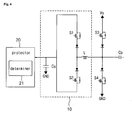
- FIG. 4 is a view for explaining an energy storage unit and a protector of the plasma display apparatus according to the embodiment of the present invention.
- FIG. 5 is a view for explaining another energy storage and protector of the plasma display apparatus according to the embodiment of the present invention.
- FIG. 6 is a view illustrating a determiner of the plasma display panel apparatus according to the embodiment of the present invention.
- FIG. 7 is a view illustrating a voltage hysteresis characteristic of an energy storage unit according to the embodiment of the present invention.
- FIG.3 is a view illustrating a plasma display apparatus according to an embodiment of the present invention.
- the plasma display apparatus of the invention comprises a plasma display panel 300, a data driver 310, a scan driver 320, and a sustain driver 330.
- the plasma display panel 300 comprises a front panel (not shown) and a rear substrate (not shown) which are assembled together. Scan electrodes Y 1 to Yn and sustain electrodes Z are formed on the front substrate, and address electrodes X 1 to Xm which intersect the scan electrodes Y 1 to Yn and the sustain electrodes Z are formed on the rear substrate.
- the data driver 310 applies data to the address electrodes X 1 to Xm formed in the plasma display panel 300.
- the data means image signal data processed from an image signal processor (not shown) for processing an image signal input from the exterior.
- the data driver 310 samples and latches data in response to a data timing control signal CTRX generated from a timing controller (not shown) and applies an address waveform having an address voltage Va to the address electrodes X 1 to Xm.
- the data driver 310 according to the embodiment of the invention comprises a protector for maintaining the address voltage Va applied to the address electrodes X 1 to Xm, that is, a voltage level of energy stored in an energy storage unit at a given range.
- the scan driver 320 drives the scan electrodes Y 1 to Yn formed in the plasma display panel 300.
- the scan driver 320 applies a setup waveform constituting a ramp-up waveform to the scan electrodes Y 1 to Yn by a combination of the sustain voltage Vs and a setup voltage Vsetup during a setup period of a reset period, in response to a scan timing control signal CTRY generated from the timing controller (not shown).
- the scan driver 320 applies a setdown waveform constituting a ramp-down waveform to the scan electrodes Y 1 to Yn.
- the scan driver 320 sequentially supplies the scan electrodes Y 1 to Yn with a scan waveform ranging from a scan reference voltage Vsc to a scan voltage -Vy.
- the scan driver 320 supplies the scan electrodes Y 1 to Yn with at least one sustain waveform for a display discharge ranging from a ground voltage level GND to a sustain voltage Vs.
- the scan driver 320 comprises a protector for maintaining the sustain voltage Vs applied to the scan electrodes Y 1 to Yn, that is, a voltage level of energy stored in an energy storage unit at a given range.
- the sustain driver 330 drives the sustain electrodes Z forming a common electrode in the plasma display panel 300.
- the sustain driver 330 applies a waveform with a positive bias voltage Vzb to the sustain electrodes Z in response to a scan timing control signal CTRZ generated from the timing controller (not shown).
- the sustain driver 330 supplies the sustain electrodes Z with at least one sustain waveform for a display discharge ranging from the ground voltage level GND to the sustain voltage Vs.
- the sustain driver 330 comprises a protector for maintaining the sustain voltage Vs applied to the sustain electrodes Z, that is, a voltage level of energy stored in an energy storage unit at a given range.
- the plasma display apparatus of the invention comprises an energy storage unit for storing the energy supplied to at least one of the address electrodes, scan electrodes and sustain electrodes, and also comprises a protector for preventing a voltage level of energy stored in the energy storage unit from deviating from a given range.
- the energy storage unit and protector may be contained in any one of the respective drivers 310, 320 and 330. Moreover, the energy storage unit and protector may be formed within the respective drivers in order to be connected to the respective electrodes or formed at the exterior of the drivers. The energy storage unit and the protector connected to the electrodes will be described with reference to FIGs. 4 and 5 .
- FIG. 4 is a view for explaining the energy storage unit and protector of the plasma display apparatus according to the embodiment of the present invention.
- the plasma display apparatus of the invention comprises a plasma display panel Cp, an energy storage unit Cs consisting substantially of a capacitor for storing an energy supplied to at least one of a plurality of electrodes formed in the plasma display panel Cp, and a protector 20 that controls the operation of a driver if the voltage of both ends of the energy storage unit Cs is beyond a predetermined voltage range so that a voltage level of energy stored in the energy storage unit Cs is maintained at the predetermined voltage range.
- the energy storage unit Cs and the protector 20 of the invention store and control the energy for driving the scan or sustain electrodes to which the sustain voltage Vs is applied among the electrodes formed in the plasma display panel Cp during the sustain period. That is, a driver of FIG. 4 corresponds to the scan driver 320 or the sustain driver 330 shown in FIG. 3
- the plasma display apparatus is provided with an energy recovery circuit 10 for recovering energy stored in the plasma display panel Cp and re-using it during the sustain period.
- the protector 20 as shown in FIG. 4 , stops the operation of a driver connected to the energy storage unit Cs if the voltage of both ends of the energy storage unit Cs in which energy recovered through the energy recovery circuit 10 is accumulated is beyond a predetermined reference range.
- the protector 20 comprises a determiner 21 for determining whether the voltage applied to both ends of the energy storage unit Cs used for a circuit device, such as a capacitor, is beyond a predetermined voltage range and blocks the operation of a switching device of a driver for supplying and recovering energy from the energy storage unit CS, i.e., of the energy recovery circuit 10 connected to the energy storage unit Cs, according to the result of determination of the determiner 21.
- a circuit device such as a capacitor
- the determiner 21 comprises at least one comparator (not shown) for comparing a voltage level of the energy storage unit Cs with a predetermined voltage. In other words, the determiner 21 senses whether the voltage level of the energy storage unit Cs is higher than a highest reference voltage or less than a lowest reference voltage by using the comparator such as an operational amplifier. Then the determiner 21 outputs a control signal for blocking a driving signal of the energy recovery circuit 10 which stores and recovers the energy in the energy storage unit Cs in order to prevent an overcharge or malfunction of the energy storage unit Cs.
- the comparator such as an operational amplifier
- the determiner 21 further comprises a compensator for previously compensating a noise component of energy supplied thereto.
- a compensator for previously compensating a noise component of energy supplied thereto.
- the protector 20 stops the operation of a switch of the energy recovery circuit 10 upon receipt of the control signal from the determiner 21.
- the protector 20 may stop the operation of first to fourth switches S 1 to S 4 operated to store energy in the energy storage unit Cs. As the first to fourth switches S 1 to S 4 are turned off, the operation of the scan or sustain driver comprising the energy recovery circuit 10 is stopped. Then the energy is not stored any more at both ends of the energy storage unit Cs and the energy stored in the energy storage unit Cs is discharged. Therefore, the voltage level of the energy storage unit Cs is lowered.
- the protector 20 stops the operation of the first to fourth switches S 1 to S 4 , thereby preventing an overcharge of the energy storage unit Cs and eliminating exposure of the energy storage unit Cs and damage to the circuit caused from the overcharging.
- the operation of the first to fourth switches S 1 to S 4 is stopped, thereby preventing the energy storage unit Cs from not recovering the energy properly due to the damage such as a short and reducing energy loss.
- a predetermined voltage range of determining the voltage level of energy stored in the energy storage unit Cs as normal differs according to the characteristics of the plasma display apparatus.
- the predetermined voltage range may be greater than 95% and less than 105% based on a predetermined reference voltage level.
- FIG. 4 illustrates a driver for supplying the sustain voltage Vs and the predetermined reference voltage level is a voltage Vs/2, substantially half the sustain voltage Vs.
- the highest reference value may be set to Vs/2+5% so that it is determined that the energy is overcharged in the energy storage unit Cs. If the voltage level of energy stored in the energy storage unit Cs is less than a half of the sustain voltage Vs by less than 5%, the lowest reference value may be set to Vs/2-5% so that it is determined that the energy storage unit Cs is damaged.
- the plasma display apparatus of the invention is for preventing the energy storage unit Cs from being exposed due to the energy overcharged therein, the highest reference value may be set to 80% of the storage capacitance of the energy storage unit Cs and the lowest reference value to 20% of the storage capacitance of the energy storage unit Cs.
- the operation of the driver may be stopped.
- the highest reference value or lowest reference value for determining that the energy storage unit Cs is in malfunction may differ according to the characteristics of the plasma display panel and of the driver, the individual specifications of each manufacturer or the internal pressure of a device used in the driver.
- FIG. 5 is a view for explaining another energy storage and protector of the plasma display apparatus according to the embodiment of the present invention.
- the plasma display apparatus of the invention comprises a plasma display panel Cp, an energy storage unit Cs consisting substantially of a capacitor for storing energy supplied to at least one of a plurality of address electrodes formed in the plasma display panel Cp, and a protector 20 that controls the operation of a driver if the voltage of both ends of the energy storage unit Cs is beyond a predetermined voltage range so that the voltage level of energy stored in the energy storage unit Cs is maintained at the predetermined voltage range.
- the energy storage unit Cs and the protector 50 of the invention store and control the energy for driving the address electrodes to which the address voltage Va is applied among the electrodes formed in the plasma display panel Cp during the address period. That is, a driver of FIG. 4 corresponds to the data driver 310 shown in FIG. 3 .
- the plasma display apparatus of an embodiment of the present invention recovers the address voltage Va supplied during the address period and re-uses it, thereby reducing power consumption and stress of the driver.
- the protector 50 controls the voltage level of energy stored in the energy storage unit Cs.
- the protector 50 has characteristics similar to the protector 20 shown in FIG. 4 . That is, the protector 50 stops the operation of a driver connected to the energy storage unit Cs if the voltage of both ends of the energy storage unit Cs in which energy recovered through the energy recovery circuit 10 is accumulated is beyond a predetermined reference range.
- the protector 50 comprises a determiner 51 and blocks the operation of a switching device of a data driver for supplying and recovering energy from the energy storage unit CS, for example, of the energy recovery circuit 10 connected to the energy storage unit Cs, according to the result of determination of the determiner 51.
- the determiner 51 comprises at least one comparator for comparing a voltage level of the energy storage unit Cs with a predetermined voltage and a compensator for previously compensating a noise component of energy input to the comparator.
- a description will be made of the compensator and the comparator shown in FIG. 5 with reference to FIG. 6 .
- the protector 50 stops the operation of first to fourth switches S 1 to S 4 , thereby preventing an overcharge of the energy storage unit Cs and eliminating exposure of the energy storage unit Cs and damage to the circuit caused from the overcharge. If the voltage level of energy stored in the energy storage unit Cs is lower than the lowest reference value, the protector 50 stops the operation of the first to fourth switches S 1 to S 4 , thereby preventing the energy storage unit Cs from not recovering the energy properly due to the damage such as a short and reducing energy loss.
- a predetermined voltage range of determining the voltage level of energy stored in the energy storage unit Cs as normal can be judged based on a voltage Va/2, half the address voltage Va. If the voltage level of energy stored in the energy storage unit Cs is greater than a half of the address voltage Va by more than 5%, the highest reference value may be set to Vs/2+5% so that it is determined that the energy is overcharged in the energy storage unit Cs. If the voltage level of energy stored in the energy storage unit Cs is less than a half of the address voltage Va by less than 5%, the lowest reference value may be set to Vs/2-5% so that it is determined that the energy storage unit Cs is damaged. Furthermore, it is possible to set the predetermined voltage range to the 20% to 80% range of the storage capacitance of the energy storage unit Cs.
- FIG. 6 illustrates a construction of the determiners 21 and 51 shown in FIGs. 4 and 5 .
- Each of the determiners 21 and 51 comprises a plurality of comparators Amp 1 to Amp 2 for determining whether a voltage applied to both ends of the capacitor Cs is beyond a predetermined reference value. That is, the comparators comprises a first operational amplifier Amp 1 for determining whether the voltage of the capacitor Cs is greater than the highest reference value and a second operational amplifier Amp 2 for determining whether the voltage of the source capacitor Cs is less than the lowest reference value.
- the determiner is comprised of the comparators using the operational amplifiers, a variety of determiners may be constructed by using various circuit devices.
- a reference voltage serving as the highest reference of a voltage chargeable in the capacitor Cs is applied to the plus (+) terminal of the first operational amplifier Amp 1 , and a voltage charged in the capacitor Cs is applied to the minus (-) terminal thereof.
- the first operational amplifier Amp 1 If a voltage of both ends of the capacitor Cs input into the minus (-) terminal is higher than the highest reference voltage applied to the plus (+) terminal, the first operational amplifier Amp 1 outputs a low signal.
- a high voltage of more than 170V is used as the sustain voltage Vs
- a high voltage of more than 80V is applied as the voltage of energy stored in the capacitor Cs.
- a reference voltage applied to the plus (+) terminal has to be increased.
- a plurality of voltage drop resistors R 1 to R 5 is connected to the input terminals of the comparators Amp 1 to Amp 2 , to thus reduce the voltage input from the capacitor Cs.
- a high resistance of K ⁇ may be used as the first resistor R1 connected to the capacitor Cs, but the degree of the resistance is not limited thereto.
- the voltage level of energy stored in the capacitor Cs is dropped by the first resistor R 1 , not a high voltage but a low voltage, proportional to the first resistor R 1 , is used as the highest reference voltage input into the plus (+) terminal.
- a resistor of 220 K ⁇ is used as the first resistor R 1 and the highest reference voltage permitted to the capacitor Cs is set to approximately 150V
- a low voltage, 1/10 the reference voltage may be applied to the plus (+) terminal.
- the voltage applied as the highest reference voltage is changeable according to the circuit configuration of the determiner.
- the first operational amplifier Amp 1 outputs a low signal, and if the voltage of the capacitor Cs is lower than the highest reference voltage, the first operational amplifier Amp 1 outputs a high signal.
- the lowest reference voltage is applied to the minus (-) terminal of the second operational amplifier Amp 2 and a voltage charged in the capacitor Cs is applied to the plus (+) terminal thereof.
- the second operational amplifier Amp 2 If the voltage of the capacitor Cs input into the plus (+) terminal of the second operational amplifier Amp 2 is lower than the lowest reference voltage, the second operational amplifier Amp 2 outputs a low signal, and if a voltage higher than the lowest reference value is charged in the capacitor Cs, the second operational amplifier Amp 2 outputs a high signal.
- a plurality of resistors may be connected between the capacitor Cs and the second operational amplifier Amp 2 so that the determiner can be driven at a low voltage, and separate terminals for applying a reference voltage to the first and second operational amplifiers Amp 1 and Amp 2 may be provided so as to compare the voltage stored in the capacitor Cs with the highest and lowest reference voltages.
- the highest and lowest reference voltages applied to the first and second operational amplifiers can be set by adjusting the resistors R 3 to R 5 as shown in FIG. 6 .
- the determiner further comprises a switching device S 5 , such as a PNP type transistor or NPN type transistor, which is conducted if an output signal output from the first and second operational amplifiers Amp 1 and Amp 2 is high and outputs a high signal of 5V by being shortcircuited if the output signal is low.
- a switching device S 5 such as a PNP type transistor or NPN type transistor, which is conducted if an output signal output from the first and second operational amplifiers Amp 1 and Amp 2 is high and outputs a high signal of 5V by being shortcircuited if the output signal is low.
- the switching device S 5 is not conducted if any one of the first and second operational amplifier Amp 1 and Amp 2 outputs a low signal.
- the output terminal of a general operational amplifier has an open collector configuration. In the event that the outputs of the first and second operational amplifiers Amp 1 and Amp 2 are linked together, if the output of one of the comparators becomes low, a low signal is applied to the switching device S 5 , thereby turning off the switching device S 5 . In contrast, a high signal is applied to the switching device S 5 only when the outputs of both comparators become high, so that the switching device S 5 is turned on.
- the determiner outputs a control signal with a high value indicating that the voltage level of energy stored in the capacitor Cs is beyond a predetermined voltage range if the switching device S 5 is turned off. In contrast, the determiner outputs a control signal with a low value indicating that the voltage level of energy stored in the capacitor Cs is within a predetermined voltage range if the switching device S 5 is turned on.
- At least one driving switching device connected to the capacitor Cs is turned off. That is, if the control signal with a high value is output from the determiner, the switching devices S 1 to S 5 within the energy recovery circuit are turned off and thus stop the applying of a voltage to the capacitor Cs.
- the control signal with a high value can be applied to all the switches S 1 to S 4 so that the operation of all the switches S 1 to S 4 of the energy recovery unit can be stopped, or to the second or third switch S 2 or S 3 so that only the operation of the second or third switch S 2 or S 3 can be stopped.
- the determiner comprises a compensator, for example, a first or second feedback resistor R f1 or R f2 for previously compensating a noise component of the energy.
- the first feedback resistor R f1 is connected to the first operational amplifier Amp 1 .
- voltage compensation occurs to the plus (+) terminal of the first operational amplifier Amp 1 to which the highest reference voltage is applied, thereby keeping a high output of the first operational amplifier Amp 1 .
- the second feedback resistor R f2 is connected to the second operational amplifier Amp 2 . If the voltage level of energy stored in the capacitor Cs becomes decreased or instantaneously decreased, voltage compensation occurs to the plus (+) terminal of the first operational amplifier Amp 2 to which the lowest reference voltage is applied, thereby keeping a high output of the second operational amplifier Amp 2 .
- the terminals of the comparators connected to the feedback resistors are not limited thereto but the determiner can be configured by connecting the feedback resistors of the minus (-) terminals of the comparators according to a circuit designer's preference.
- FIG. 7 is a view illustrating a voltage hysteresis characteristic of the energy storage unit according to the embodiment of the present invention.
- the determiner shown in FIG. 6 can be configured in such a manner to prevent the output of the determiner from being changed by noise.
- an unstable region is a voltage level when the voltage level of energy stored in the capacitor is beyond a predetermined voltage range.
- a low output is a control signal generated when the determiner determines that the voltage level of the capacitor is within a predetermined voltage range, i.e., a stable region.
- a high output is a control signal generated when the determiner determines that the voltage level of the capacitor is beyond a predetermined voltage range, i.e., an unstable region.
- the feedback resistor has hysteresis characteristics for compensating a high output to a low output in order to prevent the determiner from outputting the high output instantaneously after outputting the low output continuously.
- the determiner of the invention prevents its control signal from being changed by noise, and reliably determines the voltage level of the capacitor, thereby improving the stability of the driver.
- the protector of the plasma display apparatus can be used for a capacitor provided at a power circuit for applying a sustain voltage Vs or an address voltage Va.
- the protector is connected to a plurality of capacitors provided at a scan driver or sustain driver for applying a sustain voltage Va to scan electrodes or sustain electrodes or to a plurality of capacitors provided at a driving board for applying an address voltage Va to address electrodes. If a voltage of both ends of the capacitors is beyond an allowable reference range, the operation of the driving board is stopped. This prevents the plasma display apparatus from being damaged by an overvoltage charged in the capacitors and a high voltage applied to the electrodes, as well as stopping the operation of the driver for applying power in the event charges are not stored in the capacitors but leaked therefrom, thereby stably driving the driver.
- the plasma display apparatus can be adapted to every kinds of capacitors provided at a driver.
Landscapes
- Engineering & Computer Science (AREA)
- Power Engineering (AREA)
- Physics & Mathematics (AREA)
- Plasma & Fusion (AREA)
- Computer Hardware Design (AREA)
- General Physics & Mathematics (AREA)
- Theoretical Computer Science (AREA)
- Control Of Indicators Other Than Cathode Ray Tubes (AREA)
Claims (17)
- Plasmaanzeigevorrichtung mit:einem Plasmaanzeigepaneel (300), in welchem eine Mehrzahl von Elektroden (X1-Xm, Y1-Yn, Z) ausgebildet sind;einer Energiespeichereinheit (Cs), die eingerichtet ist, an die Elektroden angelegte Energie zu speichern; undeiner Schutzeinrichtung (20, 50), die eingerichtet ist, das Spannungsniveau der in der Energiespeichereinheit (Cs) gespeicherten Energie innerhalb eines vorherbestimmten Spannungsbereichs aufrecht zu erhalten, wobei die Schutzeinrichtung eine Ermittlungseinrichtung (21, 51) aufweist, die eingerichtet ist zu ermitteln, ob das Spannungsniveau der in der Energiespeichereinheit (Cs) gespeicherten Energie außerhalb des vorherbestimmten Spannungsbereichs liegt, und den Betrieb eines Treibers zur Zuführung oder Rückgewinnung der Energie aus der Energiespeichereinheit (Cs) je nach Ermittlung der Ermittlungseinrichtung (21, 51) zu blockieren.
- Plasmaanzeigevorrichtung nach Anspruch 1, wobei der vorherbestimmte Spannungsbereich bei 95% bis 105% eines vorherbestimmten Referenzspannungsniveaus liegt.
- Plasmaanzeigevorrichtung nach Anspruch 2, wobei das Referenzspannungsniveau im Wesentlichen halb so hoch wie eine Erhaltungsspannung (Vs) ist.
- Plasmaanzeigevorrichtung nach Anspruch 2, wobei das Referenzspannungsniveau im Wesentlichen halb so hoch wie eine Adressspannung (Va) ist.
- Plasmaanzeigevorrichtung nach Anspruch 1, wobei die Ermittlungseinrichtung (21, 51) mindestens einen Komparator (Amp1, Amp2) aufweist, der eingerichtet ist, das Spannungsniveau der in der Energiespeichereinheit (Cs) gespeicherten Energie mit dem vorherbestimmten Spannungsbereich zu vergleichen.
- Plasmaanzeigevorrichtung nach Anspruch 5, wobei die Ermittlungseinrichtung (21, 51) weiters eine Ausgleichseinrichtung (Rf1, Rf2) zum Ausgleichen einer Rauschkomponente der an die Vergleichseinrichtung (Amp1, Amp2) angelegten Energie aufweist.
- Plasmaanzeigevorrichtung nach Anspruch 1, wobei die Energiespeichereinheit (Cs) eingerichtet ist, Energie für die Ansteuerung einer Abtastelektrode (Y1-Yn) oder einer Erhaltungselektrode (Z) aus der Mehrzahl von Elektroden zu speichern.
- Plasmaanzeigevorrichtung nach Anspruch 1, wobei die Energiespeichereinheit (Cs) eingerichtet ist, Energie für die Ansteuerung einer Adresselektrode (X1-Xm) aus der Mehrzahl von Elektroden zu speichern.
- Plasmaanzeigevorrichtung nach einem der Ansprüche 5 oder 6, wobei die Energiespeichereinheit (Cs) aufweist:einen Kondensator, wobei der mindestens eine Komparator mit dem Kondensator verbunden und eingerichtet ist, das Spannungsniveau des Kondensators (Cs) mit einem vorherbestimmten Spannungsbereich zu vergleichen, undMittel zum Abschalten von mindestens einer mit dem Kondensator (Cs) verbundenen Treiber-Schalteinrichtung (S1-S4) entsprechend dem Vergleichsergebnis des Komparators (Amp1, Amp2).
- Plasmaanzeigevorrichtung nach Anspruch 9, wobei der Komparator (Amp1, Amp2) aufweist:einen ersten Operationsverstärker (Amp1), der eingerichtet ist, das Spannungsniveau mit dem höchsten Wert des vorherbestimmten Spannungsbereichs zu vergleichen; undeinen zweiten Operationsverstärker (Amp2) , der eingerichtet ist, das Spannungsniveau mit dem niedrigsten Wert des vorherbestimmten Spannungsbereichs zu vergleichen.
- Plasmaanzeigevorrichtung nach Anspruch 6 und Anspruch 10, wobei die Ausgleichseinrichtung (Rf1, Rf2) einen Rückkopplungswiderstand (Pf1.Rf2) aufweist, der mit dem ersten (Amp1) oder dem zweiten (Amp2) Operationsverstärker verbunden ist.
- Plasmaanzeigevorrichtung nach Anspruch 10, wobei der erste Operationsverstärker (Amp1) oder der zweite Operationsverstärker (Amp2) mit einem Vorwiderstand (R1-R5) zur Absenkung der Eingangsspannung verbunden ist.
- Plasmaanzeigevorrichtung nach Anspruch 9, wobei der Kondensator (Cs) eingerichtet ist, eine Erhaltungsspannung (Vs) an eine Abtastelektrode (Y1-Yn) oder eine Erhaltungselektrode (Z) aus der Mehrzahl von Elektroden anzulegen.
- Plasmaanzeigevorrichtung nach Anspruch 9, wobei der Kondensator (Cs) eingerichtet ist, eine Adressspannung (Va) an eine Adresselektrode (X1-Xm) aus der Mehrzahl von Elektroden anzulegen.
- Verfahren zum Ansteuern einer Plasmaanzeigevorrichtung mit einer Mehrzahl von Elektroden (X1-Xm, Y1-Yn, Z), umfassend die folgenden Schritte:Ermitteln, ob die Spannung der in einem Kondensator (Cs) zum Speichern von den Elektroden zugeführter Energie innerhalb eines vorherbestimmten Spannungsbereichs liegt; undStoppen eines Betriebs zum Ansteuern der Mehrzahl von Elektroden (X1-Xm, Y1-Yn, Z), wenn die Spannung der Energie außerhalb des vorherbestimmten Spannungsbereichs liegt.
- Verfahren nach Anspruch 15, wobei der Kondensator (Cs) eingerichtet ist, eine Erhaltungsspannung (Vs) an eine Abtastelektrode (Y1-Yn) oder eine Erhaltungselektrode (Z) aus der Mehrzahl von Elektroden anzulegen.
- Verfahren nach Anspruch 9, wobei der Kondensator eingerichtet ist, eine Addressspannung (Va) an eine Adresselektrode (X1-Xm) aus der Mehrzahl von Elektroden anzulegen.
Applications Claiming Priority (2)
| Application Number | Priority Date | Filing Date | Title |
|---|---|---|---|
| KR1020040096977A KR100609750B1 (ko) | 2004-11-24 | 2004-11-24 | 플라즈마 디스플레이 패널의 에너지 회수장치 |
| KR1020050042758A KR100707455B1 (ko) | 2005-05-21 | 2005-05-21 | 플라즈마 디스플레이 패널 구동장치 및 그 구동방법 |
Publications (2)
| Publication Number | Publication Date |
|---|---|
| EP1667098A1 EP1667098A1 (de) | 2006-06-07 |
| EP1667098B1 true EP1667098B1 (de) | 2012-03-21 |
Family
ID=36123239
Family Applications (1)
| Application Number | Title | Priority Date | Filing Date |
|---|---|---|---|
| EP05257245A Expired - Lifetime EP1667098B1 (de) | 2004-11-24 | 2005-11-24 | Plasmaanzeigevorrichtung und Verfahren zu ihrer Ansteuerung mit Energierückgewinnungsschaltung und Schutzschaltung |
Country Status (2)
| Country | Link |
|---|---|
| US (1) | US7633467B2 (de) |
| EP (1) | EP1667098B1 (de) |
Families Citing this family (9)
| Publication number | Priority date | Publication date | Assignee | Title |
|---|---|---|---|---|
| CN101390147B (zh) * | 2006-02-13 | 2010-09-29 | 松下电器产业株式会社 | 等离子显示面板驱动电路及等离子显示装置 |
| KR100800499B1 (ko) * | 2006-07-18 | 2008-02-04 | 엘지전자 주식회사 | 플라즈마 디스플레이 장치 |
| KR100787462B1 (ko) * | 2006-11-21 | 2007-12-26 | 삼성에스디아이 주식회사 | 플라즈마 표시장치 |
| KR20080054013A (ko) * | 2006-12-12 | 2008-06-17 | 엘지전자 주식회사 | 플라즈마 디스플레이 장치 |
| KR100831018B1 (ko) * | 2007-05-03 | 2008-05-20 | 삼성에스디아이 주식회사 | 플라즈마 표시 장치 및 그 구동 방법 |
| KR100814824B1 (ko) * | 2007-05-03 | 2008-03-20 | 삼성에스디아이 주식회사 | 플라즈마 표시 장치 및 그 구동 방법 |
| KR100879288B1 (ko) * | 2007-08-09 | 2009-01-16 | 삼성에스디아이 주식회사 | 플라즈마 표시 장치 및 그 구동 방법 |
| CN101802896B (zh) * | 2007-09-20 | 2013-07-31 | 欧丽安株式会社 | 用于等离子体显示面板的能量恢复电路 |
| KR102393410B1 (ko) | 2015-07-06 | 2022-05-03 | 삼성디스플레이 주식회사 | 전류 센서 및 그를 포함하는 유기전계발광 표시장치 |
Family Cites Families (10)
| Publication number | Priority date | Publication date | Assignee | Title |
|---|---|---|---|---|
| JPH03261377A (ja) * | 1990-03-09 | 1991-11-21 | Toshiba Corp | 電力変換装置の保護装置 |
| GB2282307A (en) * | 1993-09-24 | 1995-03-29 | Ibm | Disabling display unit when image is unchanged |
| JP3080064B2 (ja) | 1998-05-01 | 2000-08-21 | 日本電気株式会社 | プラズマディスプレイパネルの駆動回路 |
| JP3369535B2 (ja) | 1999-11-09 | 2003-01-20 | 松下電器産業株式会社 | プラズマディスプレイ装置 |
| KR20010077740A (ko) * | 2000-02-08 | 2001-08-20 | 박종섭 | 디스플레이 패널의 전력 절감회로 |
| KR20020075627A (ko) | 2001-03-26 | 2002-10-05 | 엘지전자 주식회사 | 에너지 회수회로의 제어장치 및 방법 |
| KR100438909B1 (ko) * | 2001-09-21 | 2004-07-03 | 엘지전자 주식회사 | 플라즈마 디스플레이 패널의 구동방법 및 장치 |
| KR100448190B1 (ko) * | 2002-01-21 | 2004-09-10 | 삼성전자주식회사 | 플라즈마 디스플레이패널장치 |
| KR100502350B1 (ko) * | 2003-04-25 | 2005-07-20 | 삼성에스디아이 주식회사 | 플라즈마 디스플레이 패널의 에너지 회수장치 및 이를구비하는 플라즈마 디스플레이 패널의 구동장치 |
| KR20050037639A (ko) * | 2003-10-20 | 2005-04-25 | 엘지전자 주식회사 | 에너지 회수장치 |
-
2005
- 2005-11-22 US US11/283,906 patent/US7633467B2/en not_active Expired - Fee Related
- 2005-11-24 EP EP05257245A patent/EP1667098B1/de not_active Expired - Lifetime
Non-Patent Citations (1)
| Title |
|---|
| DONG Y LEE ET AL: "Novel energy-recovery driving circuit for plasma display panel using regenerative transformer", PESC'03. 2003 IEEE 34TH. ANNUAL POWER ELECTRONICS SPECIALISTS CONFERENCE. CONFERENCE PROCEEDINGS. ACAPULCO, MEXICO, JUNE 15 - 19, 2003; [ANNUAL POWER ELECTRONICS SPECIALISTS CONFERENCE], NEW YORK, NY :; IEEE, US, vol. 2, 15 June 2003 (2003-06-15), pages 656 - 659, XP010648888, ISBN: 978-0-7803-7754-7 * |
Also Published As
| Publication number | Publication date |
|---|---|
| EP1667098A1 (de) | 2006-06-07 |
| US20060109214A1 (en) | 2006-05-25 |
| US7633467B2 (en) | 2009-12-15 |
Similar Documents
| Publication | Publication Date | Title |
|---|---|---|
| EP1667098B1 (de) | Plasmaanzeigevorrichtung und Verfahren zu ihrer Ansteuerung mit Energierückgewinnungsschaltung und Schutzschaltung | |
| KR20020062136A (ko) | 플라즈마 디스플레이 장치 및 그 제어 방법 | |
| US20050099364A1 (en) | Energy recovery apparatus and method of a plasma display panel | |
| US6710550B2 (en) | Plasma display panel apparatus and method of protecting an over current thereof | |
| CN100555368C (zh) | 等离子显示设备及其驱动方法 | |
| KR100612508B1 (ko) | 플라즈마 표시 패널의 구동 장치 | |
| CN1326102C (zh) | 用于驱动等离子体显示面板的装置和方法 | |
| KR20010028539A (ko) | 에너지 회수 장치 | |
| KR100589249B1 (ko) | 플라즈마 디스플레이 패널의 에너지 회수장치 및 회수방법 | |
| KR100707455B1 (ko) | 플라즈마 디스플레이 패널 구동장치 및 그 구동방법 | |
| US20070236415A1 (en) | Plasma Display Apparatus and Driving Method of Plasma Display Apparatus | |
| EP1837846B1 (de) | Plasmaanzeigevorrichtung | |
| US7710352B2 (en) | Plasma display panel comprising energy recovery circuit and driving method thereof | |
| US20060284799A1 (en) | Plasma display apparatus | |
| KR100450218B1 (ko) | 플라즈마 디스플레이 패널의 구동 장치 및 그 구동 방법 | |
| KR100492186B1 (ko) | 플라즈마 디스플레이 패널 | |
| JP4793013B2 (ja) | プラズマディスプレイ装置 | |
| KR100676756B1 (ko) | 플라즈마 디스플레이 패널의 집적된 어드레스 구동 회로모듈, 구동 장치 및 구동방법 | |
| KR100701966B1 (ko) | 플라즈마 디스플레이 장치 | |
| KR20040110687A (ko) | 플라즈마 디스플레이 패널의 구동회로 제어방법 및 장치 | |
| KR100823475B1 (ko) | 플라즈마 표시 장치 및 그 구동 장치 | |
| KR20080001874A (ko) | 플라즈마 디스플레이 장치 | |
| JP4848790B2 (ja) | プラズマディスプレイ装置 | |
| KR100867577B1 (ko) | 플라즈마 디스플레이 장치 | |
| KR100553936B1 (ko) | 에너지 회수장치 및 방법 |
Legal Events
| Date | Code | Title | Description |
|---|---|---|---|
| PUAI | Public reference made under article 153(3) epc to a published international application that has entered the european phase |
Free format text: ORIGINAL CODE: 0009012 |
|
| 17P | Request for examination filed |
Effective date: 20051205 |
|
| AK | Designated contracting states |
Kind code of ref document: A1 Designated state(s): AT BE BG CH CY CZ DE DK EE ES FI FR GB GR HU IE IS IT LI LT LU LV MC NL PL PT RO SE SI SK TR |
|
| AX | Request for extension of the european patent |
Extension state: AL BA HR MK YU |
|
| 17Q | First examination report despatched |
Effective date: 20070112 |
|
| AKX | Designation fees paid |
Designated state(s): DE FR GB NL |
|
| GRAP | Despatch of communication of intention to grant a patent |
Free format text: ORIGINAL CODE: EPIDOSNIGR1 |
|
| RIN1 | Information on inventor provided before grant (corrected) |
Inventor name: CHO, JANGHWAN Inventor name: KIM, JINYOUNG Inventor name: JUNG, YUNKWON Inventor name: CHOI, DONG KWON Inventor name: KWON, CHANGYOUNG Inventor name: PARK, DONGHYUK Inventor name: AN, YANG KI |
|
| GRAS | Grant fee paid |
Free format text: ORIGINAL CODE: EPIDOSNIGR3 |
|
| GRAA | (expected) grant |
Free format text: ORIGINAL CODE: 0009210 |
|
| AK | Designated contracting states |
Kind code of ref document: B1 Designated state(s): DE FR GB NL |
|
| REG | Reference to a national code |
Ref country code: GB Ref legal event code: FG4D |
|
| REG | Reference to a national code |
Ref country code: DE Ref legal event code: R096 Ref document number: 602005033250 Country of ref document: DE Effective date: 20120524 |
|
| REG | Reference to a national code |
Ref country code: NL Ref legal event code: T3 |
|
| PLBE | No opposition filed within time limit |
Free format text: ORIGINAL CODE: 0009261 |
|
| STAA | Information on the status of an ep patent application or granted ep patent |
Free format text: STATUS: NO OPPOSITION FILED WITHIN TIME LIMIT |
|
| 26N | No opposition filed |
Effective date: 20130102 |
|
| PGFP | Annual fee paid to national office [announced via postgrant information from national office to epo] |
Ref country code: NL Payment date: 20121015 Year of fee payment: 8 |
|
| REG | Reference to a national code |
Ref country code: DE Ref legal event code: R097 Ref document number: 602005033250 Country of ref document: DE Effective date: 20130102 |
|
| GBPC | Gb: european patent ceased through non-payment of renewal fee |
Effective date: 20121124 |
|
| REG | Reference to a national code |
Ref country code: FR Ref legal event code: ST Effective date: 20130731 |
|
| PG25 | Lapsed in a contracting state [announced via postgrant information from national office to epo] |
Ref country code: GB Free format text: LAPSE BECAUSE OF NON-PAYMENT OF DUE FEES Effective date: 20121124 Ref country code: FR Free format text: LAPSE BECAUSE OF NON-PAYMENT OF DUE FEES Effective date: 20121130 |
|
| PGFP | Annual fee paid to national office [announced via postgrant information from national office to epo] |
Ref country code: DE Payment date: 20131015 Year of fee payment: 9 |
|
| REG | Reference to a national code |
Ref country code: NL Ref legal event code: V1 Effective date: 20140601 |
|
| PG25 | Lapsed in a contracting state [announced via postgrant information from national office to epo] |
Ref country code: NL Free format text: LAPSE BECAUSE OF NON-PAYMENT OF DUE FEES Effective date: 20140601 |
|
| REG | Reference to a national code |
Ref country code: DE Ref legal event code: R119 Ref document number: 602005033250 Country of ref document: DE |
|
| PG25 | Lapsed in a contracting state [announced via postgrant information from national office to epo] |
Ref country code: DE Free format text: LAPSE BECAUSE OF NON-PAYMENT OF DUE FEES Effective date: 20150602 |