EP1643596A2 - Verbindungsstruktur - Google Patents
Verbindungsstruktur Download PDFInfo
- Publication number
- EP1643596A2 EP1643596A2 EP05027017A EP05027017A EP1643596A2 EP 1643596 A2 EP1643596 A2 EP 1643596A2 EP 05027017 A EP05027017 A EP 05027017A EP 05027017 A EP05027017 A EP 05027017A EP 1643596 A2 EP1643596 A2 EP 1643596A2
- Authority
- EP
- European Patent Office
- Prior art keywords
- interconnect
- pair
- interconnect structure
- planar
- interconnects
- Prior art date
- Legal status (The legal status is an assumption and is not a legal conclusion. Google has not performed a legal analysis and makes no representation as to the accuracy of the status listed.)
- Withdrawn
Links
Images


Classifications
-
- H—ELECTRICITY
- H05—ELECTRIC TECHNIQUES NOT OTHERWISE PROVIDED FOR
- H05K—PRINTED CIRCUITS; CASINGS OR CONSTRUCTIONAL DETAILS OF ELECTRIC APPARATUS; MANUFACTURE OF ASSEMBLAGES OF ELECTRICAL COMPONENTS
- H05K3/00—Apparatus or processes for manufacturing printed circuits
- H05K3/36—Assembling printed circuits with other printed circuits
- H05K3/368—Assembling printed circuits with other printed circuits parallel to each other
-
- H—ELECTRICITY
- H01—ELECTRIC ELEMENTS
- H01R—ELECTRICALLY-CONDUCTIVE CONNECTIONS; STRUCTURAL ASSOCIATIONS OF A PLURALITY OF MUTUALLY-INSULATED ELECTRICAL CONNECTING ELEMENTS; COUPLING DEVICES; CURRENT COLLECTORS
- H01R12/00—Structural associations of a plurality of mutually-insulated electrical connecting elements, specially adapted for printed circuits, e.g. printed circuit boards [PCB], flat or ribbon cables, or like generally planar structures, e.g. terminal strips, terminal blocks; Coupling devices specially adapted for printed circuits, flat or ribbon cables, or like generally planar structures; Terminals specially adapted for contact with, or insertion into, printed circuits, flat or ribbon cables, or like generally planar structures
- H01R12/50—Fixed connections
- H01R12/51—Fixed connections for rigid printed circuits or like structures
- H01R12/52—Fixed connections for rigid printed circuits or like structures connecting to other rigid printed circuits or like structures
-
- H—ELECTRICITY
- H01—ELECTRIC ELEMENTS
- H01L—SEMICONDUCTOR DEVICES NOT COVERED BY CLASS H10
- H01L2224/00—Indexing scheme for arrangements for connecting or disconnecting semiconductor or solid-state bodies and methods related thereto as covered by H01L24/00
- H01L2224/01—Means for bonding being attached to, or being formed on, the surface to be connected, e.g. chip-to-package, die-attach, "first-level" interconnects; Manufacturing methods related thereto
- H01L2224/42—Wire connectors; Manufacturing methods related thereto
- H01L2224/47—Structure, shape, material or disposition of the wire connectors after the connecting process
- H01L2224/48—Structure, shape, material or disposition of the wire connectors after the connecting process of an individual wire connector
- H01L2224/4805—Shape
- H01L2224/4809—Loop shape
- H01L2224/48091—Arched
-
- H—ELECTRICITY
- H01—ELECTRIC ELEMENTS
- H01L—SEMICONDUCTOR DEVICES NOT COVERED BY CLASS H10
- H01L2224/00—Indexing scheme for arrangements for connecting or disconnecting semiconductor or solid-state bodies and methods related thereto as covered by H01L24/00
- H01L2224/01—Means for bonding being attached to, or being formed on, the surface to be connected, e.g. chip-to-package, die-attach, "first-level" interconnects; Manufacturing methods related thereto
- H01L2224/42—Wire connectors; Manufacturing methods related thereto
- H01L2224/47—Structure, shape, material or disposition of the wire connectors after the connecting process
- H01L2224/49—Structure, shape, material or disposition of the wire connectors after the connecting process of a plurality of wire connectors
- H01L2224/491—Disposition
- H01L2224/4911—Disposition the connectors being bonded to at least one common bonding area, e.g. daisy chain
- H01L2224/49111—Disposition the connectors being bonded to at least one common bonding area, e.g. daisy chain the connectors connecting two common bonding areas, e.g. Litz or braid wires
-
- H—ELECTRICITY
- H01—ELECTRIC ELEMENTS
- H01L—SEMICONDUCTOR DEVICES NOT COVERED BY CLASS H10
- H01L2924/00—Indexing scheme for arrangements or methods for connecting or disconnecting semiconductor or solid-state bodies as covered by H01L24/00
- H01L2924/10—Details of semiconductor or other solid state devices to be connected
- H01L2924/11—Device type
- H01L2924/13—Discrete devices, e.g. 3 terminal devices
- H01L2924/1304—Transistor
- H01L2924/1306—Field-effect transistor [FET]
- H01L2924/13091—Metal-Oxide-Semiconductor Field-Effect Transistor [MOSFET]
-
- H—ELECTRICITY
- H05—ELECTRIC TECHNIQUES NOT OTHERWISE PROVIDED FOR
- H05K—PRINTED CIRCUITS; CASINGS OR CONSTRUCTIONAL DETAILS OF ELECTRIC APPARATUS; MANUFACTURE OF ASSEMBLAGES OF ELECTRICAL COMPONENTS
- H05K1/00—Printed circuits
- H05K1/02—Details
- H05K1/0213—Electrical arrangements not otherwise provided for
- H05K1/0216—Reduction of cross-talk, noise or electromagnetic interference
-
- H—ELECTRICITY
- H05—ELECTRIC TECHNIQUES NOT OTHERWISE PROVIDED FOR
- H05K—PRINTED CIRCUITS; CASINGS OR CONSTRUCTIONAL DETAILS OF ELECTRIC APPARATUS; MANUFACTURE OF ASSEMBLAGES OF ELECTRICAL COMPONENTS
- H05K1/00—Printed circuits
- H05K1/02—Details
- H05K1/14—Structural association of two or more printed circuits
- H05K1/145—Arrangements wherein electric components are disposed between and simultaneously connected to two planar printed circuit boards, e.g. Cordwood modules
-
- H—ELECTRICITY
- H05—ELECTRIC TECHNIQUES NOT OTHERWISE PROVIDED FOR
- H05K—PRINTED CIRCUITS; CASINGS OR CONSTRUCTIONAL DETAILS OF ELECTRIC APPARATUS; MANUFACTURE OF ASSEMBLAGES OF ELECTRICAL COMPONENTS
- H05K1/00—Printed circuits
- H05K1/02—Details
- H05K1/14—Structural association of two or more printed circuits
- H05K1/148—Arrangements of two or more hingeably connected rigid printed circuit boards, i.e. connected by flexible means
-
- H—ELECTRICITY
- H05—ELECTRIC TECHNIQUES NOT OTHERWISE PROVIDED FOR
- H05K—PRINTED CIRCUITS; CASINGS OR CONSTRUCTIONAL DETAILS OF ELECTRIC APPARATUS; MANUFACTURE OF ASSEMBLAGES OF ELECTRICAL COMPONENTS
- H05K1/00—Printed circuits
- H05K1/16—Printed circuits incorporating printed electric components, e.g. printed resistor, capacitor, inductor
- H05K1/162—Printed circuits incorporating printed electric components, e.g. printed resistor, capacitor, inductor incorporating printed capacitors
-
- H—ELECTRICITY
- H05—ELECTRIC TECHNIQUES NOT OTHERWISE PROVIDED FOR
- H05K—PRINTED CIRCUITS; CASINGS OR CONSTRUCTIONAL DETAILS OF ELECTRIC APPARATUS; MANUFACTURE OF ASSEMBLAGES OF ELECTRICAL COMPONENTS
- H05K2201/00—Indexing scheme relating to printed circuits covered by H05K1/00
- H05K2201/07—Electric details
- H05K2201/0776—Resistance and impedance
- H05K2201/0792—Means against parasitic impedance; Means against eddy currents
-
- H—ELECTRICITY
- H05—ELECTRIC TECHNIQUES NOT OTHERWISE PROVIDED FOR
- H05K—PRINTED CIRCUITS; CASINGS OR CONSTRUCTIONAL DETAILS OF ELECTRIC APPARATUS; MANUFACTURE OF ASSEMBLAGES OF ELECTRICAL COMPONENTS
- H05K2201/00—Indexing scheme relating to printed circuits covered by H05K1/00
- H05K2201/09—Shape and layout
- H05K2201/09209—Shape and layout details of conductors
- H05K2201/09654—Shape and layout details of conductors covering at least two types of conductors provided for in H05K2201/09218 - H05K2201/095
- H05K2201/09672—Superposed layout, i.e. in different planes
-
- H—ELECTRICITY
- H05—ELECTRIC TECHNIQUES NOT OTHERWISE PROVIDED FOR
- H05K—PRINTED CIRCUITS; CASINGS OR CONSTRUCTIONAL DETAILS OF ELECTRIC APPARATUS; MANUFACTURE OF ASSEMBLAGES OF ELECTRICAL COMPONENTS
- H05K2201/00—Indexing scheme relating to printed circuits covered by H05K1/00
- H05K2201/10—Details of components or other objects attached to or integrated in a printed circuit board
- H05K2201/10227—Other objects, e.g. metallic pieces
- H05K2201/1028—Thin metal strips as connectors or conductors
-
- H—ELECTRICITY
- H05—ELECTRIC TECHNIQUES NOT OTHERWISE PROVIDED FOR
- H05K—PRINTED CIRCUITS; CASINGS OR CONSTRUCTIONAL DETAILS OF ELECTRIC APPARATUS; MANUFACTURE OF ASSEMBLAGES OF ELECTRICAL COMPONENTS
- H05K2201/00—Indexing scheme relating to printed circuits covered by H05K1/00
- H05K2201/10—Details of components or other objects attached to or integrated in a printed circuit board
- H05K2201/10613—Details of electrical connections of non-printed components, e.g. special leads
- H05K2201/10742—Details of leads
- H05K2201/1075—Shape details
- H05K2201/10818—Flat leads
-
- H—ELECTRICITY
- H05—ELECTRIC TECHNIQUES NOT OTHERWISE PROVIDED FOR
- H05K—PRINTED CIRCUITS; CASINGS OR CONSTRUCTIONAL DETAILS OF ELECTRIC APPARATUS; MANUFACTURE OF ASSEMBLAGES OF ELECTRICAL COMPONENTS
- H05K2201/00—Indexing scheme relating to printed circuits covered by H05K1/00
- H05K2201/10—Details of components or other objects attached to or integrated in a printed circuit board
- H05K2201/10613—Details of electrical connections of non-printed components, e.g. special leads
- H05K2201/10742—Details of leads
- H05K2201/10886—Other details
- H05K2201/10893—Grouped leads, i.e. element comprising multiple leads distributed around but not through a common insulator
-
- H—ELECTRICITY
- H05—ELECTRIC TECHNIQUES NOT OTHERWISE PROVIDED FOR
- H05K—PRINTED CIRCUITS; CASINGS OR CONSTRUCTIONAL DETAILS OF ELECTRIC APPARATUS; MANUFACTURE OF ASSEMBLAGES OF ELECTRICAL COMPONENTS
- H05K3/00—Apparatus or processes for manufacturing printed circuits
- H05K3/36—Assembling printed circuits with other printed circuits
Definitions
- the present invention relates to an interconnect structure making connection, for example, between circuit boards.
- An electrical circuit is sometimes implemented using a two-layer circuit board structure.
- interconnection between the lower level and the upper level of the circuit has been achieved by using stiff wires, with a row of mutually parallel interconnections disposed on one side of a circuit board.
- an interconnect structure comprises: a first interconnect comprising a body portion configured as a first planer conductor with a first plane, in a four-sided form having a first side, a second side, a third side opposing the first side, and a fourth side, the first side crossing the second side, with a first vertex therebetween, the third side crossing the second side, with a second vertex therebetween, a first connecting portion configured on the first side, in a vicinity of the first vertex, and a second connecting portion configured on the third side, in a vicinity of the second vertex; and a second interconnect comprising a body portion configured as a second planer conductor with a second plane close and parallel to the first plane, in a four-sided form having a fifth side, a sixth side parallel to the second side, a seventh side opposing the fifth side, and an eighth side, the fifth side crossing the eighth side, with a third vertex therebetween, the seventh side crossing the eighth side, with a fourth vertex
- an interconnect structure comprises: a first interconnect comprising a body portion configured as a first planer conductor with a first plane, in a four-sided form having a first side, a second side, a third side opposing the first side, and a fourth side, the first side crossing the fourth side, with a first vertex therebetween, the third side crossing the second side, with a second vertex therebetween, a first connecting portion configured on the first side, in a vicinity of the first vertex, and a second connecting portion configured on the third side, in a vicinity of the second vertex; and a second interconnect comprising a body portion configured as a second planer conductor with a second plane close and parallel to the first plane, in a four-sided form having a fifth side, a sixth side parallel to the second side, a seventh side opposing the fifth side, and an eighth side, the fifth side crossing the sixth side, with a third vertex therebetween, the seventh side crossing the eighth side, with a fourth vertex
- an interconnect structure comprises a plurality of layered interconnects having mutually flush sides, the plurality of layered interconnects each respectively comprising: a body portion configured as a planer conductor with a pair of planes, in a four-sided form including a pair of opposing sides; and a pair of connecting portions configured either on both of the pair of opposing sides.
- Fig. 1 is a perspective view showing a first embodiment of the present invention.
- the reference numerals 1 and 2 denote planar interconnects for implementing the present invention, and A and B are circuit boards, which are disposed in mutually parallel opposition.
- Connection terminals 1A and 1B for making connection to prescribed interconnections on circuit boards A and B are located at both ends of the planar interconnect 1, and similarly connection terminals 2A and 2B are located at both ends of the planar interconnect 2.
- the planar interconnects 1 and 2 are, for example, made of a copper sheet having a thickness of 0.2 mm, and are disposed with a very small spacing therebetween, for example approximately 0.2 mm.
- Fig. 1 is a perspective view and, in order to make the positions of the planar interconnects clearly visible, they are drawn intentionally with a shift therebetween. This comment applies to other drawings to be used in subsequent descriptions to follow. Mounting is facilitated by making the widths of the connection terminals small in order to make connections to the circuit boards, and so that there is no mutual interference therebetween.
- an interconnect structure comprises: a first interconnect 1 which comprises a body portion 1a configured as a first planer conductor with a first plane (the front side), in a four-sided form that has a top first side 41, a left second side 42, a bottom third side 43 opposing the first side 41, and a right fourth side 44, the first side 41 crossing the second side 42, with a left upper first vertex 45 therebetween, the third side 43 crossing the second side 42, with a left lower second vertex 46 therebetween, an upward first connecting portion 1B configured on the first side 41, in a vicinity of the first vertex 45, and a downward second connecting portion 1A configured on the third side 43, in a vicinity of the second vertex 46; and a second interconnect 2 which comprises a body portion 2a configured as a second planer conductor with a second plane (the rear side) close and parallel to the first plane of the first interconnect 1, in a four-sided form that has a top top fifth side 51, a left
- the circuit board A has mounted thereon, for example: a central wide planer drain line 10 connected at its right end to a lower end of a vertical terminal 14 formed with a fixing hole 14a for external connection at the top; a long planer source line 11 connected at a rear end thereof to the lower terminal 1A of the planer interconnect 1, and at the right end to a lower end of another vertical terminal 13 formed with a fixing hole 13a for external connection at the top; a short planer gate line 12 connected on a rear half thereof to the lower terminal 2A of the planer interconnect 2; and a semiconductor chip 20 as a set of power supply MOS transistors having, on the upside, a gate electrode 21 connected by a bonding wire 22 to a front half of the gate line 12 and source electrodes 23 connected by bonding wires 24 to a front part of the source line 11, and at the downside, a drain electrode connected to the drain line 10.
- a central wide planer drain line 10 connected at its right end to a lower end of a vertical terminal 14 formed with a fixing
- the circuit board B has mounted thereon, for example, a capacitor 31, a resistor 32, a coil 33, and a transistor 34.
- a first advantage that can be cited is an increase in the line-to-line capacitance between planar interconnects, so that the interconnects themselves serve as a filter to absorb high-frequency noise, thereby enabling a reduction in the high-frequency noise included in a signal.
- FIG. 3 we see an example of an invention, in which the positions of the connection terminals on the circuit board B side of Fig. 1 have been reversed. Specifically, this has the effect of making currents flowing between the upper and the lower circuit boards cross as they flow through the planar interconnects.
- the interconnect structure of the past in order to achieve such a crossing of currents it was absolutely necessary either to carefully place rigid wire interconnects so as to impart a twist thereto, to use a jumper wire on a circuit board, to use a multiple-layer circuit board, or to make a major diversion of interconnects.
- the achievement of this crossing of currents requires absolutely no technical difficulty with regard to structure.
- an interconnect structure comprises: a first interconnect 1 which comprises a body portion configured as a first planer conductor with a first plane (the front side), in a four-sided form that has a top first side, a left second side, a bottom third side opposing the first side, and a right fourth side, the first side crossing the fourth side, with a right upper first vertex therebetween, the third side crossing the second side, with a left lower second vertex therebetween, a first connecting portion 1B configured on the first side, in a vicinity of the first vertex, and a second connecting portion 1A configured on the third side, in a vicinity of the second vertex; and a second interconnect 2 which comprises a body portion configured as a second planer conductor with a second plane (the rear side) close and parallel to the first plane, in a four-sided form that has a top fifth side, a left sixth side parallel to the second side of the first interconnect 1, a bottom seventh side opposing the fifth side, and a
- Fig. 2 is a graph showing the results of calculating the size of the interconnect partial inductance alone, in the prior art and in the present invention.
- the horizontal axis represents the distance between connection terminals, normalized with respect to the distance between two circuit boards.
- the white circles show the case of the present invention as illustrated by the example of Fig. 1
- the black circles show the case of the present invention as illustrated by the example of Fig. 3
- white squares show the prior art
- the black squares show the case of a round-trip path with crossing as used in the past.
- an alternate configuration of the present invention is one in which a plurality of connection terminals are provided on one end or both ends of one planar interconnect.
- the connection terminals 1A and 1A' serve also as a jumper wire on the circuit board A of the first-level circuit board A, without relationship to the connection terminal 1B.
- the circuitry within the circuit board A is simplified, thereby enabling effective use of the circuit board surface area.
- the planar interconnect 1 and the planar interconnect 2 close together, the line-to-line capacitance therebetween increases, thereby enabling the interconnect structure to function as a noise filter.
- it is effective to interpose a material having a high dielectric coefficient between the planar interconnects 1 and 2, unrelated to the purpose of achieving insulation therebetween.
- an interconnect structure of Fig. 1 or Fig. 3 further comprises a fifth connecting portion 1A' or 2B' configured on one of the first side, the third side, the fifth side, and the seventh side.
- Fig. 5 shows the use of four planar interconnects as an example of yet another embodiment of the present invention.
- the reference numerals 1, 2, 3, and 4 each represent planar interconnects.
- an interconnect structure comprises an arbitrary combination of interconnects shown in Fig. 1, Fig. 3, and/or Fig. 4.
- an interconnect structure comprising that of Fig. 1, and a third interconnect 3 which comprises a body portion configured as a third planer conductor with a third plane close and parallel to one of the first and second planes, in a four-sided form having a ninth side, a tenth side parallel to the second side, an eleventh side opposing the ninth side, and a twelfth side side, the ninth side crossing the tenth side, with a fifth vertex therebetween, the eleventh side crossing the twelfth side, with a sixth vertex therebetween, a fifth connecting portion 3B configured on the ninth side, in a vicinity of the fifth vertex, and a sixth connecting portion 3A configured on the eleventh side, in a vicinity of the sixth vertex.
- an interconnect structure comprising that of Fig. 3 and a fourth interconnect 4 which comprises a body portion configured as a fourth planer conductor with a third plane close and parallel to one of the first and second planes, in a four-sided form having a ninth side, a tenth side parallel to the second side, an eleventh side opposing the ninth side, and a twelfth side, the ninth side crossing the twelfth side, with a fifth vertex therebetween, the eleventh side crossing the twelfth side, with a sixth vertex therebetween, a fifth connecting portion 4B configured on the ninth side, in a vicinity of the fifth vertex, and a sixth connecting portion 4A configured on the eleventh side, in a vicinity of the sixth vertex.
- a fourth interconnect 4 which comprises a body portion configured as a fourth planer conductor with a third plane close and parallel to one of the first and second planes, in a four-sided form having a ninth side, a tenth side parallel to the second side,
- connection terminals shown in the foregoing cited drawings are disposed on opposing sides of a rectangular planar interconnect, it will be understood that this is not an intrinsic feature of the present invention.
- the connection terminals 1A and 4A' extend outward at a prescribed angle from each planar interconnect side (the planar interconnect in this case being vertical), and make connections at positions that are at a distance from the main part of the planar interconnect.
- this type of arrangement it is possible to establish an independently supported structure as the planar interconnect, and to simplify the mounting process.
- an interconnect structure of any of Fig. 1 to Fig. 5 further comprises another connecting portion 1A or 4A' configured on one of the second side and the fourth side.
- planar interconnects are not restricted to flat planar shapes, and can alternatively be, for example, a shape formed by truncating a cylindrical shape with a plane parallel to the center axis of the cylinder.
- an interconnect structure comprises a plurality of layered interconnects 1, 2, 3, and 4 having mutually flush sides (the above-noted second sides), the plurality of layered interconnects each respectively comprising a body portion configured as a planer conductor with a pair of planes, in a four-sided form including a pair of opposing sides, and a pair of connecting portions 1A, 1B; 2A, 2B; 3A, 3B; or 4A, 4B configured either on both of the pair of opposing sides.
- the plurality of layered interconnects may include any and all interconnects shown in Fig. 1 to Fig. 6.
- Fig. 8 is a perspective view showing yet another embodiment of the present invention.
- crossing of currents does not occur between the planar interconnects 2 and 3 in the embodiment shown in Fig. 5, it is possible as shown in Fig. 8 to form both on one and the same plane, thereby enabling savings in thickness of the overall interconnect structure.
- connection terminal 1B in Fig. 9 is shown as being slightly smaller than the length of the upper side of the planar interconnect, it can alternatively be made the same as the width of the planar interconnect. Although not shown in the drawing, it is possible to have both the connection terminals 1A and 1B make connection to the circuit boards with a large width.
- Fig. 8 shows an interconnect structure according to the aspect implemented in Fig. 7, wherein the plurality of layered interconnects includes: a first interconnect 1 of which the four-sided form of the body portion has a first pair of remaining sides (i.e., left and right sides) thereof spaced at a first distance from each other; a second interconnect 2 of which the four-sided form of the body portion has a second pair of remaining sides (i.e., left and right sides) thereof spaced from each other at a second distance smaller than the first distance, the second pair of remaining sides including one remaining side (i.e., the left side) being flush with one (i.e., the left side) of the first pair of remaining sides; and a third interconnect 3 of which the four-sided form of the body portion has a third pair of remaining sides (i.e., left and right sides) spaced from each other at a third distance smaller than the first distance, the third pair of remaining sides including one remaining side (i.e.
- Fig. 10 shows an interconnect structure according to the aspect implemented in Fig. 7, wherein the four-sided form has a pair of remaining sides (i.e. front and rear sides in the figure) bent at right angles.
- connection terminals appear arranged laterally along one side of a circuit board, and for a circuit board that in use is inserted into a slot, by adopting a configuration in which interconnections are made between two circuit boards inserted into different slots, it is possible to achieve the same type of effects as described for other arrangements of circuit boards.
- Fig. 11 shows an interconnect structure according to the aspect implemented in Fig. 7, wherein the four-sided form has a pair of remaining sides (i.e. front and rear sides in the figure) bent at right angles at different locations thereon.
- FIG. 12 Yet another configuration, as illustrated in Fig. 12, is one in which an L-shaped planar interconnect structure as noted above has an L shape when viewed from a direction that is perpendicular to mutually parallel circuit boards A and B, in which case, because the planar interconnect structure stands independently on the circuit board A, mounting by soldering or the like is facilitated.
- the L-shaped planar interconnect structure is either provided near the center of gravity of the upper circuit board B or provided at two locations thereon, it is possible to support the upper circuit board B using the planar interconnect structure itself.
- the above-noted two locations can be at diagonally opposing positions of the circuit board and, of course, it is possible to dispose this structure at three or even four comers of the circuit board.
- Fig. 12 shows an interconnect structure according to the aspect implemented in Fig. 7, wherein the four-sided form has the pair of opposing sides (i.e. top and bottom in the figure) bent at right angles.
- FIG. 13 shows an interconnect structure according to the aspect implemented in Fig. 7, wherein the four-sided form has the pair of opposing sides (i.e. top and bottom in the figure) bent at right angles at different locations thereon.
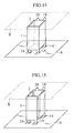
- FIG. 14 Another possible configuration, as shown in Fig. 14, is one in which a planar interconnect has a tubular shape (either cylindrical or square), and yet another is one, as shown in Fig. 15, in which a nearly tubular structure not having an annular structure and having an open end is used.
- a tubular shape or a tubular shape with an open end if this structure is used, for example, for a power supply line and a ground line and the configuration is arranged so that it surrounds the periphery of the circuit board, because the overall configuration has a box shape, immunity is achieved on the power supply with respect to externally introduced electromagnetic noise, it is possible to suppress the generation of noise to the outside, and it is further possible to achieve a great improvement in the degree of freedom in designing the power supply line on the circuit board.
- Fig. 16 the reference numerals 2 and 3, similar to the case shown in Fig. 8, denote two planar interconnects inserted in an arrangement so that there is no crossing of currents therein. Additionally, in this configuration, if necessary it is possible to have partial interconnects interposed between the two circuit boards. If this is done, there are relatively few jumper wires on the circuit boards, making it possible to supply electrical power with at a low impedance.
- Fig. 14 shows an interconnect structure according to the aspect implemented in Fig. 7, wherein the four-sided form has the pair of opposing sides each respectively deformed into a polygonal enclosing form, which is close.
- Fig. 15 shows an interconnect structure according to the aspect implemented in Fig. 7, wherein the four-sided form has the pair of opposing sides each respectively deformed into a polygonal enclosing form, which is open.
- Fig. 16 shows an interconnect structure according to the aspect implemented in Fig. 7, wherein the plurality of layered interconnects are configured to be cooperative to define an polygonal enclosing form.
- the present invention has various aspects to be noted.
- a first aspect of the present invention is an interconnect structure having a plurality of planar interconnects interposed with a prescribed distance therebetween, each planar interconnect having at least two connection terminals, and each planar interconnect having at least two sets of sides capable of existing in one and the same plane in mutual proximal opposition.
- the configuration of this aspect of the present invention corresponds to that shown in Fig. 1 of the accompanying drawings, which is described below. Taking the example shown in Fig. 1, one set of sides that can exist in one and the same plane are the upper side of the planar interconnect 1 and the upper side of the planar interconnect 2 in Fig.
- planar interconnect 1 and the planar interconnect 2 of Fig. 1 another set of sides that can exist in one and the same plane are the lower sides of the planar interconnect 1 and the planar interconnect 2 of Fig. 1, making a total of two sets of such sides.
- the above-used phrase "in one and the same plane" refers, for example, to the two lower sides of the two planar interconnects facing the circuit board A, and the upper sides thereof facing the circuit board B.
- planar interconnect shall not be construed herein to be restricted to a flat planar shape, and shall encompass, for example, a shape formed by truncating a cylindrical shape with a plane parallel to the center axis of the cylinder.
- Another aspect of the present invention is a variation on the first aspect, wherein a straight line joining one connection terminal existing at a side belonging to one of two sets of sides in one planar interconnect of the plurality of planar interconnects and a straight line joining one connection terminal existing at a side belonging to one of two sets of sides in another of the plurality of planar interconnects intersect when viewed from a direction perpendicular to a main surface of the plurality of planar interconnects.
- the configuration of this aspect of the present invention corresponds to that shown, by way of example, in Fig. 3, which is described below. In the example shown in Fig.
- the straight line joining the connection terminals 1A and 1B of the planar interconnect 1 and the straight line joining the connection terminals 2A and 2B of the planar interconnect 2 appear to intersect one another when viewed from a direction that is perpendicular to the surfaces of the planar interconnects 1 and 2, this being from the direction of the viewer of the drawing.
- a current path joining the lower right connection terminal 2A and the upper left connection terminal is formed by the planar interconnect 1 and a current path joining the lower left connection terminal 1A and the upper right connection terminal 1B is formed by the planar interconnect 2.
- this branching structure can be achieved by application of the interconnection structure provided by the present invention. That is, application of the present invention simplifies circuit board interconnections and enables effective use of circuit board real estate, while enabling a reduction in the interconnection impedance formed on the circuit boards.
- a third aspect of the present invention is a variation on either the first aspect or the second aspect, wherein there are three or more planar interconnects, of which at least two are electrically connected, and of which at least one planar interconnect is interposed between other planar interconnects.
- the configuration of this aspect of the present invention corresponds, for example, to those shown in Fig. 4 and Fig. 7, which are described below.
- the two planar interconnects are connected to a ground line or a power supply line and the planar interconnect interposed therebetween is a signal line, it is possible to protect the signal line from the introduction of external electromagnetic noise, and also to suppress the generation of electromagnetic noise from the signal line.
- a fourth aspect of the present invention is a variation on either the first or the second aspect, wherein there are a second and a third planar interconnect adjacent to a main surface of a first planar interconnect.
- the configuration of this aspect of the present invention corresponds, for example, to that shown in Fig. 8, to be described below. Taking the example shown in Fig. 8, the planar interconnects 2 and 3 are disposed in a row in one and the same plane facing the planar interconnect 1.
- the adoption of this configuration can be done to limit the overall thickness of the interconnection structure. Additionally, in this case the mutual inductance between the second interconnect and the third interconnect is reduced by the effect of eddy currents generated in the first interconnect.
- a fifth aspect of the present invention is a variation on any one of the first to the fourth aspects, wherein one or all of the planar interconnects has an L shape, a square channel shape, a tubular shape, or a tubular shape having an open end.
- Examples of an L-shaped planar interconnect are shown in Fig. 10 and Fig. 12
- examples of a square channel planar interconnect are shown in Fig. 11 and Fig. 13, and an example of a openended tubular shape is shown in Fig. 15.
- the tubular shape having an open end need not be a completely closed tube, but rather can have a partial opening. It will be understood that the tubular shape referred to above encompasses both a round cylindrical shape and a rectangular tubular shape.
- the interconnect structure itself provides support for the circuit boards it connects, thereby enhancing the degree of freedom in designing the overall apparatus.
- a sixth aspect of the present invention is a variation on any one of the first to the fifth aspects, wherein a high dielectric substance is interposed between a plurality of planar interconnects. This configuration is described below with reference made to, for example, Fig. 1 and Fig. 6.
- interposing a high dielectric substance between planar interconnects not only facilitates insulation between a plurality of planar interconnects, but also increases the line-to-line capacitances, thereby further enhancing the noise filtering effect.
- This invention relates to an interconnect structure comprising: a first interconnect comprising: a body portion configured as a first planer conductor with a first plane, in a four-sided form having a first side, a second side, a third side opposing the first side, and a fourth side, the first side crossing the second side, with a first vertex therebetween, the third side crossing the second side, with a second vertex therebetween; a first connecting portion configured on the first side, in a vicinity of the first vertex; and a second connecting portion configured on the third side, in a vicinity of the second vertex; and a second interconnect comprising: a body portion configured as a second planer conductor with a second plane close and parallel to the first plane, in a four-sided form having a fifth side, a sixth side parallel to the second side, a seventh side opposing the fifth side, and an eighth side, the fifth side crossing the eighth side, with a third vertex therebetween, the seventh side crossing the eighth side, with a fourth vertex
- the interconnect structure is further comprising a fifth connecting portion configured on one of the first side, the third side, the fifth side, and the seventh side.
- the interconnect structure is further comprising a third interconnect comprising: a body portion configured as a third planer conductor with a third plane close and parallel to one of the first and second planes, in a four-sided form having a ninth side, a tenth side parallel to the second side, an eleventh side opposing the ninth side, and a twelfth side side, the ninth side crossing the tenth side, with a fifth vertex therebetween, the eleventh side crossing the twelfth side, with a sixth vertex therebetween; a fifth connecting portion configured on the ninth side, in a vicinity of the fifth vertex; and a sixth connecting portion configured on the eleventh side, in a vicinity of the sixth vertex.
- a third interconnect comprising: a body portion configured as a third planer conductor with a third plane close and parallel to one of the first and second planes, in a four-sided form having a ninth side, a tenth side parallel to the second side, an eleventh side opposing the ninth side,
- the interconnect structure is further comprising a fifth connecting portion configured on one of the second side and the fourth side.
- This invention relates further to an interconnect structure comprising: a first interconnect comprising: a body portion configured as a first planer conductor with a first plane, in a four-sided form having a first side, a second side, a third side opposing the first side, and a fourth side, the first side crossing the fourth side, with a first vertex therebetween, the third side crossing the second side, with a second vertex therebetween; a first connecting portion configured on the first side, in a vicinity of the first vertex; and a second connecting portion configured on the third side, in a vicinity of the second vertex; and a second interconnect comprising: a body portion configured as a second planer conductor with a second plane close and parallel to the first plane, in a four-sided form having a fifth side, a sixth side parallel to the second side, a seventh side opposing the fifth side, and an eighth side, the fifth side crossing the sixth side, with a third vertex therebetween, the seventh side crossing the eighth side, with a fourth ver
- the interconnect structure is further comprising a fifth connecting portion configured on one of the first side, the third side, the fifth side, and the seventh side.
- the interconnect structure is further comprising a third interconnect comprising: a body portion configured as a third planer conductor with a third plane close and parallel to one of the first and second planes, in a four-sided form having a ninth side, a tenth side parallel to the second side, an eleventh side opposing the ninth side, and a twelfth side, the ninth side crossing the twelfth side, with a fifth vertex therebetween, the eleventh side crossing the twelfth side, with a sixth vertex therebetween; a fifth connecting portion configured on the ninth side, in a vicinity of the fifth vertex; and a sixth connecting portion configured on the eleventh side, in a vicinity of the sixth vertex.
- a third interconnect comprising: a body portion configured as a third planer conductor with a third plane close and parallel to one of the first and second planes, in a four-sided form having a ninth side, a tenth side parallel to the second side, an eleventh side opposing the ninth side
- the interconnect structure is further comprising a fifth connecting portion configured on one of the second side and the fourth side.
- This invention relates further to an interconnect structure comprising a plurality of layered interconnects having mutually flush sides, the plurality of layered interconnects each respectively comprising: a body portion configured as a planer conductor with a pair of planes, in a four-sided form having a pair of opposing sides; and a pair of connecting portions configured either on both of the first pair of opposing sides.
- the plurality of layered interconnects includes: a first interconnect of which the four-sided form of the body portion has a first pair of remaining sides thereof spaced at a first distance from each other; a second interconnect of which the four-sided form of the body portion has a second pair of remaining sides thereof spaced from each other at a second distance smaller than the first distance, the second pair of remaining sides including one remaining side being flush with one of the first pair of remaining sides; and a third interconnect of which the four-sided form of the body portion has a third pair of remaining sides thereof spaced from each other at a third distance smaller than the first distance, the third pair of remaining sides including one remaining side being flush with the other of the first pair of remaining sides.
- the four-sided form has a pair of remaining sides bent at right angles.
- the four-sided form has a pair of remaining sides bent at right angles at different locations thereon.
- the four-sided form has the pair of opposing sides bent at right angles.
- the four-sided form has the pair of opposing sides bent at right angles at different locations thereon.
- the four-sided form has the pair of opposing sides each respectively deformed into an enclosing form.
- the enclosing form is close.
- the enclosing form is open.
- the plurality of layered interconnects are configured to be cooperative to define an enclosing form.
Landscapes
- Engineering & Computer Science (AREA)
- Manufacturing & Machinery (AREA)
- Microelectronics & Electronic Packaging (AREA)
- Combinations Of Printed Boards (AREA)
- Structure Of Printed Boards (AREA)
Applications Claiming Priority (2)
| Application Number | Priority Date | Filing Date | Title |
|---|---|---|---|
| JP2000282945A JP3826696B2 (ja) | 2000-09-19 | 2000-09-19 | 配線構造 |
| EP01122202A EP1191635B1 (de) | 2000-09-19 | 2001-09-17 | Verbindungsstruktur |
Related Parent Applications (1)
| Application Number | Title | Priority Date | Filing Date |
|---|---|---|---|
| EP01122202A Division EP1191635B1 (de) | 2000-09-19 | 2001-09-17 | Verbindungsstruktur |
Publications (1)
| Publication Number | Publication Date |
|---|---|
| EP1643596A2 true EP1643596A2 (de) | 2006-04-05 |
Family
ID=18767370
Family Applications (2)
| Application Number | Title | Priority Date | Filing Date |
|---|---|---|---|
| EP01122202A Expired - Lifetime EP1191635B1 (de) | 2000-09-19 | 2001-09-17 | Verbindungsstruktur |
| EP05027017A Withdrawn EP1643596A2 (de) | 2000-09-19 | 2001-09-17 | Verbindungsstruktur |
Family Applications Before (1)
| Application Number | Title | Priority Date | Filing Date |
|---|---|---|---|
| EP01122202A Expired - Lifetime EP1191635B1 (de) | 2000-09-19 | 2001-09-17 | Verbindungsstruktur |
Country Status (4)
| Country | Link |
|---|---|
| US (1) | US6641407B2 (de) |
| EP (2) | EP1191635B1 (de) |
| JP (1) | JP3826696B2 (de) |
| DE (1) | DE60137387D1 (de) |
Cited By (1)
| Publication number | Priority date | Publication date | Assignee | Title |
|---|---|---|---|---|
| EP2113967A3 (de) * | 2008-04-29 | 2011-06-29 | Siemens Aktiengesellschaft | Anordnung zweier Schaltungsträger |
Families Citing this family (19)
| Publication number | Priority date | Publication date | Assignee | Title |
|---|---|---|---|---|
| US7631242B2 (en) | 2001-06-22 | 2009-12-08 | Broadcom Corporation | System, method and computer program product for mitigating burst noise in a communications system |
| DE10336634B3 (de) * | 2003-08-08 | 2005-02-03 | Siemens Ag | Elektronisches Gerät |
| WO2005119765A2 (en) * | 2004-06-02 | 2005-12-15 | Tessera, Inc. | Assembly including vertical and horizontal joined circuit panels |
| US7658621B2 (en) * | 2008-04-17 | 2010-02-09 | Hon Hai Precision Ind. Co., Ltd. | Connector assembly having connecting device |
| US20100254109A1 (en) | 2009-03-19 | 2010-10-07 | Olympus Corporation | Mount assembly and method for manufacturing mount assembly |
| DE102009017621B3 (de) * | 2009-04-16 | 2010-08-19 | Semikron Elektronik Gmbh & Co. Kg | Vorrichtung zur Verringerung der Störabstrahlung in einem leistungselektronischen System |
| JP5097791B2 (ja) * | 2010-04-05 | 2012-12-12 | 株式会社日立産機システム | 電力変換装置 |
| GB2484742B (en) * | 2010-10-22 | 2013-06-12 | Murata Power Solutions Milton Keynes Ltd | Electronic component for surface mounting |
| JPWO2013121732A1 (ja) * | 2012-02-15 | 2015-05-11 | パナソニックIpマネジメント株式会社 | 無線モジュール |
| JP5946339B2 (ja) * | 2012-06-27 | 2016-07-06 | 双信電機株式会社 | ノイズフィルタ |
| KR102034717B1 (ko) * | 2013-02-07 | 2019-10-21 | 삼성전자주식회사 | 파워모듈용 기판, 파워모듈용 터미널 및 이들을 포함하는 파워모듈 |
| US9837380B2 (en) | 2014-01-28 | 2017-12-05 | Infineon Technologies Austria Ag | Semiconductor device having multiple contact clips |
| US9468103B2 (en) * | 2014-10-08 | 2016-10-11 | Raytheon Company | Interconnect transition apparatus |
| JP2016092024A (ja) * | 2014-10-29 | 2016-05-23 | 株式会社豊田自動織機 | 電子機器 |
| US9660333B2 (en) | 2014-12-22 | 2017-05-23 | Raytheon Company | Radiator, solderless interconnect thereof and grounding element thereof |
| US9780458B2 (en) | 2015-10-13 | 2017-10-03 | Raytheon Company | Methods and apparatus for antenna having dual polarized radiating elements with enhanced heat dissipation |
| US10361485B2 (en) | 2017-08-04 | 2019-07-23 | Raytheon Company | Tripole current loop radiating element with integrated circularly polarized feed |
| US10923830B2 (en) * | 2019-01-18 | 2021-02-16 | Pc-Tel, Inc. | Quick solder chip connector for massive multiple-input multiple-output antenna systems |
| TW202142517A (zh) * | 2020-05-12 | 2021-11-16 | 台灣愛司帝科技股份有限公司 | 基板拼接結構、基板拼接系統以及基板拼接方法 |
Family Cites Families (7)
| Publication number | Priority date | Publication date | Assignee | Title |
|---|---|---|---|---|
| US4878862A (en) * | 1988-12-05 | 1989-11-07 | Amp Incorporated | Connector for mating two bus bars |
| US5037311A (en) * | 1989-05-05 | 1991-08-06 | International Business Machines Corporation | High density interconnect strip |
| FR2753310B1 (fr) * | 1996-09-12 | 1998-12-31 | Gandois Jean Marie | Dispositif d'alimentation electrique par plinthe sans pose de cables |
| US5825633A (en) * | 1996-11-05 | 1998-10-20 | Motorola, Inc. | Multi-board electronic assembly including spacer for multiple electrical interconnections |
| GB9713849D0 (en) * | 1997-06-30 | 1997-09-03 | Amp Italia | Capacitance coupled cross-talk suppressing communication connector |
| DE29805943U1 (de) * | 1998-03-26 | 1998-06-10 | Abb Daimler Benz Transp | Niederinduktive Verschienung zweier mehrlagiger Stromschienenanordnungen für Stromrichter |
| US6468090B2 (en) * | 1999-09-15 | 2002-10-22 | Fci Americas Technology, Inc. | Low inductance power connector and method of reducing inductance in an electrical connector |
-
2000
- 2000-09-19 JP JP2000282945A patent/JP3826696B2/ja not_active Expired - Fee Related
-
2001
- 2001-09-17 EP EP01122202A patent/EP1191635B1/de not_active Expired - Lifetime
- 2001-09-17 DE DE60137387T patent/DE60137387D1/de not_active Expired - Lifetime
- 2001-09-17 EP EP05027017A patent/EP1643596A2/de not_active Withdrawn
- 2001-09-19 US US09/955,302 patent/US6641407B2/en not_active Expired - Fee Related
Cited By (1)
| Publication number | Priority date | Publication date | Assignee | Title |
|---|---|---|---|---|
| EP2113967A3 (de) * | 2008-04-29 | 2011-06-29 | Siemens Aktiengesellschaft | Anordnung zweier Schaltungsträger |
Also Published As
| Publication number | Publication date |
|---|---|
| JP2002094209A (ja) | 2002-03-29 |
| EP1191635A2 (de) | 2002-03-27 |
| JP3826696B2 (ja) | 2006-09-27 |
| US20020037656A1 (en) | 2002-03-28 |
| EP1191635B1 (de) | 2009-01-14 |
| EP1191635A3 (de) | 2003-10-15 |
| US6641407B2 (en) | 2003-11-04 |
| DE60137387D1 (de) | 2009-03-05 |
Similar Documents
| Publication | Publication Date | Title |
|---|---|---|
| US6641407B2 (en) | Conductor interconnect structure connecting circuit boards | |
| US7042303B2 (en) | Energy conditioning circuit assembly | |
| US6509807B1 (en) | Energy conditioning circuit assembly | |
| JP5995723B2 (ja) | 基準回路を有する多層回路部材 | |
| JP4292652B2 (ja) | パワー半導体モジュール | |
| JP4826845B2 (ja) | パワー半導体モジュール | |
| KR101010876B1 (ko) | 관통 콘덴서의 설치 구조 | |
| US5731960A (en) | Low inductance decoupling capacitor arrangement | |
| KR100427111B1 (ko) | 에너지 조절 회로 조립체 | |
| US20230253341A1 (en) | Circuit module | |
| JP2018137440A (ja) | 基板回路装置及びプリント配線基板 | |
| CN220233160U (zh) | 电路模块 | |
| JP2002057418A (ja) | プリント配線基板 | |
| JP4086963B2 (ja) | パワーモジュール | |
| JP2010098162A (ja) | プリント配線基板および設計支援システム | |
| US11133243B2 (en) | Electronic device and wiring board | |
| US6906910B1 (en) | Structures for implementing integrated conductor and capacitor in SMD packaging | |
| WO2012153835A1 (ja) | プリント配線基板 | |
| JP6256575B2 (ja) | 高周波モジュール | |
| JP6425632B2 (ja) | プリント基板 | |
| US20220159834A1 (en) | Module | |
| JPH05235258A (ja) | トランジスタモジュール | |
| JP2011146454A (ja) | ノイズ対策構造 | |
| US11889616B2 (en) | Circuit board | |
| US8139369B2 (en) | Printed wiring board solder pad arrangement |
Legal Events
| Date | Code | Title | Description |
|---|---|---|---|
| PUAI | Public reference made under article 153(3) epc to a published international application that has entered the european phase |
Free format text: ORIGINAL CODE: 0009012 |
|
| 17P | Request for examination filed |
Effective date: 20051209 |
|
| AC | Divisional application: reference to earlier application |
Ref document number: 1191635 Country of ref document: EP Kind code of ref document: P |
|
| AK | Designated contracting states |
Kind code of ref document: A2 Designated state(s): DE FR GB |
|
| STAA | Information on the status of an ep patent application or granted ep patent |
Free format text: STATUS: THE APPLICATION HAS BEEN WITHDRAWN |
|
| 18W | Application withdrawn |
Effective date: 20091030 |