EP1633006A2 - Leuchtdiode und Verfahren zu ihrer Herstellung - Google Patents
Leuchtdiode und Verfahren zu ihrer Herstellung Download PDFInfo
- Publication number
- EP1633006A2 EP1633006A2 EP05106750A EP05106750A EP1633006A2 EP 1633006 A2 EP1633006 A2 EP 1633006A2 EP 05106750 A EP05106750 A EP 05106750A EP 05106750 A EP05106750 A EP 05106750A EP 1633006 A2 EP1633006 A2 EP 1633006A2
- Authority
- EP
- European Patent Office
- Prior art keywords
- light
- supporting member
- emitting diode
- leads
- metal plate
- Prior art date
- Legal status (The legal status is an assumption and is not a legal conclusion. Google has not performed a legal analysis and makes no representation as to the accuracy of the status listed.)
- Withdrawn
Links
Images


Classifications
-
- H—ELECTRICITY
- H10—SEMICONDUCTOR DEVICES; ELECTRIC SOLID-STATE DEVICES NOT OTHERWISE PROVIDED FOR
- H10H—INORGANIC LIGHT-EMITTING SEMICONDUCTOR DEVICES HAVING POTENTIAL BARRIERS
- H10H20/00—Individual inorganic light-emitting semiconductor devices having potential barriers, e.g. light-emitting diodes [LED]
- H10H20/80—Constructional details
- H10H20/85—Packages
- H10H20/8506—Containers
-
- H—ELECTRICITY
- H10—SEMICONDUCTOR DEVICES; ELECTRIC SOLID-STATE DEVICES NOT OTHERWISE PROVIDED FOR
- H10H—INORGANIC LIGHT-EMITTING SEMICONDUCTOR DEVICES HAVING POTENTIAL BARRIERS
- H10H20/00—Individual inorganic light-emitting semiconductor devices having potential barriers, e.g. light-emitting diodes [LED]
- H10H20/80—Constructional details
- H10H20/85—Packages
- H10H20/857—Interconnections, e.g. lead-frames, bond wires or solder balls
Definitions
- the present invention relates to a light-emitting diode that is mounted on a circuit substrate and in particular, to a surface mounting-type (SMT) light-emitting diode that comprises a projectile-type dome part or lens parts.
- SMT surface mounting-type
- An example of this type of light-emitting diode is a light-emitting diode wherein two or more metal plate leads connected to LED chips (light-emitting elements) are bent along the horizontal folds at the base end of the resin dome part (or the projectile-type lens part) and surface mounting-type connecting parts are made in the plate surface facing the circuit substrate (JP (Kokai) Unexamined Patent Publication 7[1995]-211,937 and JP Unexamined Patent Publication 2003-8070).
- the placement and surface area of the plate surface that contacts the circuit substrate are selected so that the light-emitting diode can be supported with stability before being connected by soldering.
- a variety of angles can be used for the bending angle, with the angle being selected in accordance with the required angle direction of the projectile-type lens parts.
- the leads are not necessarily bent in the same direction; three or more leads can even be mounted on the circuit substrate with stability by bending some leads in a direction opposite that of other leads.
- an object of the present invention is to provide a surface mounting-type light-emitting diode with projectile-type dome parts that can be easily produced at a low height, and a method for its production.
- Another object of the present invention is to provide a light-emitting diode that does not require a bending treatment after the dome part is formed during the production process and therefore there is no detrimental effect on the dome part or on the connecting parts between the leads and the LED chips, and the like.
- the present invention provides a light-emitting diode comprising at least a pair (that is, two) metal plate leads connected to light-emitting elements and connecting terminals of surface mounting-type connecting parts at the edges of these metal sheet leads.
- the light-emitting diode further comprises a supporting member that contacts a mounted circuit substrate and, together with the metal plate leads, supports the light-emitting diode with stability on the circuit substrate before connection by soldering.
- the supporting member is anchored to at least part of the metal plate leads.
- the supporting member extends in the direction that intersects with the pair of leads to provide proper supporting means at pre-determined positions.
- the supporting member can comprise a mechanical engagement means for aligning the metal plate leads and supporting legs in the direction of height.
- the supporting member is made from metal plates and, as with the pair of leads, at the base ends, has surface mounting-type connecting parts for connection to so-called connection pads on a circuit substrate.
- the supporting member can be anchored to the base ends of a transparent resin dome part of the light-emitting diode.
- the supporting member can be engaged with a mold cup for molding such that this end is prevented from turning during molding of the dome part and are aligned in the direction of height, and then anchored with the dome part that has been molded by resin molding.
- the present invention further provides a method for producing a light-emitting diode.
- the production method comprises a step for forming the lead frame of metal plate leads with surface mounting parts, a step for connecting and disposing light-emitting elements at the top end of the metal plate leads of each unit that forms the light-emitting diode, and a step for forming a resin molded article such that the light-emitting elements are enclosed, and in particular, the step for forming the lead frame includes a step for forming the surface mounting parts at the edges of the metal plate leads, and further comprises a step for joining a supporting member having supporting legs that, together with the metal sheet leads, supports the light-emitting diode on a circuit substrate. It is preferred that the step for joining the supporting member is performed before or simultaneously with the step for forming the resin molded article.
- the process for joining the supporting member comprises a step for joining a supporting member to metal plate leads.
- the supporting member is made from metal plates and the step for joining the supporting member can comprise a step for anchoring the supporting member to only one lead of the pair of the metal plate leads where a light-emitting element is disposed in each unit of the lead frame.
- the step for joining the supporting member comprises a step whereby the supporting member is engaged with the molding cup for resin molded articles and the supporting member is anchored by molding of the resin molded article.
- Figures 1 and 2 are drawings showing a first preferred embodiment of the light-emitting diode of the present invention.
- Figure 1 shows a completed light-emitting diode
- Figure 2 shows the diode with the supporting member removed from the lead in order to understand this structure.
- Figure (a) in each figure is the front view and (b) is the side view.
- a light-emitting diode 10 comprises a pair of leads 20 and 30 made from metal plates; a light-emitting element 40 is anchored to the inside of a cup 21 at the top end of lead 20; a dome part 90 formed by resin molding such that light-emitting element 40 is enclosed; and a supporting member 70 that engages with lead 20.
- Light-emitting element 40 is, for instance, a semiconductor element in the form of a light-emitting diode chip.
- the inside surface of cup 21 where light-emitting element 40 is positioned is inclined and has the effect of reflecting up the diffused light emitted from light-emitting element 40.
- a top end face 91 of dome part 90 has a convex curved surface that acts as a lens for focusing the light from light-emitting element 40.
- light-emitting element 40 is connected to lead 30 by a bonded metal wire that is not illustrated. In another case, depending on the structure of light-emitting element 40, lead 20 and light-emitting element 40 are connected by wire bonding.
- the pair of leads 20 and 30 electrically connected to light-emitting element 40 comprises surface mounting-type connecting parts 25 and 35 that extend from the base ends of dome part 90 and connect with an outside circuit substrate that is not illustrated.
- Connecting parts 25 and 35 include legs 26 and 36 that extend in a perpendicular direction and connecting ends 27 and 37 at the bottom ends thereof.
- Connecting parts 25 and 35 form the metal plate surfaces that are the same as the primary parts positioned inside dome part 90 without being bent.
- connecting ends 27 and 37 have long thin parts extending horizontally and are made so that the edges of the metal plates at these long thin parts face the circuit substrate (not illustrated) on which light-emitting diode 10 will be mounted.
- Supporting member 70 works with leads 20 and 30 such that when light-emitting diode 10 is mounted on a circuit substrate (that is not illustrated), light-emitting diode 10 is supported with stability on the circuit substrate during reflow, and during other steps.
- supporting member 70 is made from a metal and engages and extends to intersect with lead 20.
- light-emitting diode 10 aligned with a pre-determined pad (not illustrated) on the circuit substrate is supported at four points by leads 20 and 30 and supporting member 70.
- supporting member 70 can also be produced from a resin rather than a metal when it is not necessary to take into consideration the effect of heat radiation that will be discussed later.
- supporting member 70 comprises at the bottom thereof surface mounting-type connecting parts 75 that comprise a pair of legs 76 and connecting ends 77 at the tips of the legs. As with connecting ends 27 and 37, connecting ends 77 are made such that they touch pads on a circuit substrate (not illustrated) along the edges of the metal sheets that form these ends. Connecting parts 75 can be soldered and connected to a circuit substrate by the same reflow technique, and similar processes that are used to connect connecting parts 25 and 35 to the circuit substrate.
- Light-emitting element 40 is directly anchored to lead 30 to which supporting member 70 is anchored as in the present embodiment; therefore, the heat generated by light-emitting element 40 escapes through supporting member 70 to the circuit substrate, or to the outside from the part of the supporting member on the base side of dome part 90. It is not always necessary to connect the connecting part 75 portion of the supporting member to the circuit substrate; light-emitting diode 10 can be supported by simply contacting the circuit substrate.
- connecting ends 27, 37, and 77 thereof be placed virtually exactly on one plane within a predetermined allowance. Consequently, supporting member 70 must be anchored to lead 20 at least with connecting parts 25, 35, and 75 accurately positioned.
- slots 22 and 72 are made in lead 20 and supporting member 70, respectively, as a means for joining the lead and the supporting member; the slots hold the metal sheet surfaces of the lead and the supporting member, resulting in mechanical engagement in an intersecting state, as shown in Figure 2.
- connecting end 27 of lead 20 and connecting end 77 of supporting member 70 are aligned precisely at least in the direction of height. Furthermore, welding, soldering, and the like can be used for the engaged portion when a stronger joint is needed between lead 20 and supporting member 70.
- connecting end 77of supporting member 70 and connecting ends 27 and 37 of leads 20 and 30 do not project close to one another (as do leads 120 and 130 in the second embodiment).
- the resin for dome part 90 is molded above supporting member 70 such that supporting member 70 extends inside dome part 90.
- a reinforcing means for mechanically strengthening the joint between supporting member 70 and the resin is realized by the present embodiment with a concave part 73 on the inside of which the resin can be held.
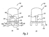
- Figure 3 is a drawing showing a second preferred embodiment of the light-emitting diode of the present invention.
- Figure (a) is a front view and (b) is a side view.
- a light-emitting diode 110 comprises a pair of leads 120 and 130; a light-emitting element 140 that is positioned inside a cup 121 at the top end of lead 120 and is electrically connected to lead 120; and a dome part 190 that is obtained by resin molding to enclose the top ends of leads 120 and 130.
- leads 120 and 130 have connecting parts 125 and 135 that extend to the base side of dome part 190 and these connecting parts are made within one plane as the primary metal plate surface of leads 120 and 130 positioned inside dome part 190.
- Connecting parts 125 and 135 comprise legs 126 and 136 near dome part 190 and connecting ends 127 and 137 wherein the metal edges serve as the connecting faces for surface mounting.
- Light-emitting diode 110 of the second embodiment differs from the first embodiment in that it comprises a ring-shaped supporting member 170, in place of a plate-shaped supporting member, which engages with the leads.
- FIG. 4 is a drawing showing the supporting member of the second embodiment of the present invention.
- Figure (a) is the plane view
- (b) is the front view
- (c) is the side view.
- Supporting member 170 comprises a ring-shaped body 171 with an opening 174; a step part 172 that projects up slightly inside body 171; legs 175 that project toward the base at a position facing body 171; and a tongue 173 projecting up from body 171 in one place.
- an overhang part 179 for instance, for differentiating between anodes and cathodes (cathode marks), and the like, is made in part of opening 174.
- the shape or color of the supporting member can be used as marking that can provide other information except differentiation of electrodes.
- Supporting member 170 is anchored at the base of dome part 190, as shown in Figure 3. Supporting member 170 is bonded facing the resin of dome part 190 along the base end of dome part 190. In further detail, supporting member 170 is placed facing the resin when dome part 190 is molded and is anchored to dome part 190 as the resin solidifies.
- a material that has good adhesion with the resin that forms dome part 190 and is heat resistant is selected as the material for supporting member 170.
- the material for supporting member 170 can be made of PPA (polyphthalamide) or another resin, or aluminum or another metal.
- PPA polyphthalamide
- Various conventional methods for modifying surface character can be used for improving adhesion with the resin of dome part 190.
- Leads 120 and 130 are placed so that they pass through opening 174 during the resin molding step.
- a step part 172 that projects above body 171 is introduced into the molding cup during molding and engages with the cup such that supporting member 170 is aligned with the axis of the light-emitting diode.
- the outside of tongue 173 engages with a groove of a complementary shape that has been made in the molding cup and the supporting member is aligned in the direction of rotation.
- the height of connecting ends 127 and 137 of leads 120 and 130 and the base end of leg 175 can be aligned with the completed light-emitting diode 110 by using step part 172 and tongue 173 that have complementary shapes that will engage with the molding cup.
- the height of leads 120 and 130 is aligned; therefore, the base end of leg 175 forms almost exactly one plane with connecting ends 127 and 137 of connecting parts 125 and 135 when supporting member 170 is in an anchored state. Consequently, light-emitting diode 110 is supported with sufficient stability by both connecting parts 125 and 135 of leads 120 and 130 and the pair of legs 175 of supporting member 170 when the light-emitting diode is placed on the circuit substrate by the reflow step or another technique for surface-mounted connection.
- a projection that engages with a through-hole or concave part in a circuit substrate can also be made in at least one of the base ends of legs 175 as an aligning means.
- the shape of the supporting member is changed and a wall that is near the base end of the dome part is made such that opening 174 becomes sufficiently small and at least the top surface of the wall is colored black, or another color, the black can be seen from the top of the dome part when the light-emitting element is not emitting light; therefore, contrast between states where the light-emitting element is on and off can be improved.
- FIG. 5 is a drawing showing a single-unit lead frame during the production steps as it relates to the leads used in the first and second embodiments.
- a unit 250 comprises a pair of leads 220 and 320. That is, leads 220 and 320 correspond to the first embodiment and leads 120 and 130 correspond to the second embodiment.
- the basic steps involved in the production of first and second light-emitting diodes 10 and 110 are the following: a step for producing a lead frame comprising a plurality of units 250 by die cutting a metal plate; a step for forming a cup 221 by pressing each unit in the lead frame to lead 220; a step for anchoring a light-emitting element inside cup 221; a step for electrically connecting the light-emitting element and the pair of leads; a step for resin molding a dome part that encloses the light-emitting element; a step for anchoring the supporting member; and a step for cutting each unit from the lead frame.
- light-emitting diode 10 in the first embodiment involves anchoring supporting member 70 to lead 20 before molding of dome part 20.
- This anchoring is realized by mechanical engagement or mechanical engagement and welding or another means, as previously mentioned.
- light-emitting diode 110 of the second embodiment is produced at the same time as dome part 190 is formed, as previously described.
- Figure 5 shows the cutting position CP for producing the final product. It is clear that metal plate parts extending horizontally are formed and surface mounting-type connecting parts 225 and 325 are made with the leads of these metal plates serving as connecting ends 227 and 327 directly above the cutting positions of leads 220 and 230. Surface mounting-type connecting parts 225 and 325 of leads 220 and 320 can be easily produced without special means.
- a supporting means for a light-emitting diode can be provided by bending and forming a metal plate to be intersected with the leads before the dome part is molded and preferably before the light-emitting element has been anchored.
Landscapes
- Led Device Packages (AREA)
Applications Claiming Priority (1)
| Application Number | Priority Date | Filing Date | Title |
|---|---|---|---|
| JP2004233084A JP2006054234A (ja) | 2004-08-10 | 2004-08-10 | 発光ダイオード及びその製造方法 |
Publications (2)
| Publication Number | Publication Date |
|---|---|
| EP1633006A2 true EP1633006A2 (de) | 2006-03-08 |
| EP1633006A3 EP1633006A3 (de) | 2008-07-23 |
Family
ID=35520634
Family Applications (1)
| Application Number | Title | Priority Date | Filing Date |
|---|---|---|---|
| EP05106750A Withdrawn EP1633006A3 (de) | 2004-08-10 | 2005-07-22 | Leuchtdiode und Verfahren zu ihrer Herstellung |
Country Status (4)
| Country | Link |
|---|---|
| US (1) | US7619260B2 (de) |
| EP (1) | EP1633006A3 (de) |
| JP (1) | JP2006054234A (de) |
| CN (1) | CN100505340C (de) |
Families Citing this family (7)
| Publication number | Priority date | Publication date | Assignee | Title |
|---|---|---|---|---|
| JP2008258530A (ja) * | 2007-04-09 | 2008-10-23 | Rohm Co Ltd | 半導体発光装置 |
| EP3138734B1 (de) * | 2015-09-03 | 2020-04-15 | SMR Patents S.à.r.l. | Lichtmodul, lichtanordnung und rückspiegelvorrichtung für ein fahrzeug |
| CN103378262B (zh) * | 2012-04-26 | 2017-02-01 | 青岛青扬众创新能源科技有限公司 | 发光二极管及其封装方法 |
| JP2015012212A (ja) * | 2013-07-01 | 2015-01-19 | 株式会社ディスコ | 発光チップ |
| JP6467206B2 (ja) * | 2014-01-28 | 2019-02-06 | 株式会社小糸製作所 | 光源ユニット |
| TWI559577B (zh) | 2014-11-06 | 2016-11-21 | 崇得電子股份有限公司 | SMT type LED package element, its manufacturing method and light emitting device |
| US12610672B1 (en) * | 2025-07-30 | 2026-04-21 | Dongguan Yisheng Electronic Technology Co., Ltd. | Through-hole LED lamp bead |
Citations (2)
| Publication number | Priority date | Publication date | Assignee | Title |
|---|---|---|---|---|
| JPH07211937A (ja) | 1994-01-14 | 1995-08-11 | Matsushita Electron Corp | 発光ダイオード |
| JP2003008070A (ja) | 2001-06-22 | 2003-01-10 | Toyoda Gosei Co Ltd | 発光ダイオード |
Family Cites Families (12)
| Publication number | Priority date | Publication date | Assignee | Title |
|---|---|---|---|---|
| JPH0685328A (ja) * | 1992-08-28 | 1994-03-25 | Stanley Electric Co Ltd | 表面実装型ledの製造方法 |
| JP3113104B2 (ja) * | 1992-11-20 | 2000-11-27 | ローム株式会社 | 半導体装置の製造方法 |
| JPH0794008A (ja) | 1993-09-24 | 1995-04-07 | Chiyatani Sangyo Kk | 面照明装置 |
| US6710373B2 (en) * | 1999-09-27 | 2004-03-23 | Shih-Yi Wang | Means for mounting photoelectric sensing elements, light emitting diodes, or the like |
| US6552368B2 (en) * | 2000-09-29 | 2003-04-22 | Omron Corporation | Light emission device |
| US6561680B1 (en) * | 2000-11-14 | 2003-05-13 | Kelvin Shih | Light emitting diode with thermally conductive structure |
| US20020070387A1 (en) * | 2000-12-07 | 2002-06-13 | Bily Wang | Focusing cup on a folded frame for surface mount optoelectric semiconductor package |
| JP2002246650A (ja) * | 2001-02-13 | 2002-08-30 | Agilent Technologies Japan Ltd | 発光ダイオード及びその製造方法 |
| KR101015289B1 (ko) * | 2002-11-05 | 2011-02-15 | 파나소닉 주식회사 | 발광다이오드 |
| JP4254214B2 (ja) | 2002-11-27 | 2009-04-15 | 日亜化学工業株式会社 | 半導体装置およびその製造方法 |
| US7420271B2 (en) * | 2003-02-20 | 2008-09-02 | Tsung Hsin Chen | Heat conductivity and brightness enhancing structure for light-emitting diode |
| TW560813U (en) * | 2003-03-06 | 2003-11-01 | Shang-Hua You | Improved LED seat |
-
2004
- 2004-08-10 JP JP2004233084A patent/JP2006054234A/ja active Pending
-
2005
- 2005-07-22 EP EP05106750A patent/EP1633006A3/de not_active Withdrawn
- 2005-07-25 US US11/188,413 patent/US7619260B2/en not_active Expired - Lifetime
- 2005-08-10 CN CN200510090208.8A patent/CN100505340C/zh not_active Expired - Fee Related
Patent Citations (2)
| Publication number | Priority date | Publication date | Assignee | Title |
|---|---|---|---|---|
| JPH07211937A (ja) | 1994-01-14 | 1995-08-11 | Matsushita Electron Corp | 発光ダイオード |
| JP2003008070A (ja) | 2001-06-22 | 2003-01-10 | Toyoda Gosei Co Ltd | 発光ダイオード |
Also Published As
| Publication number | Publication date |
|---|---|
| EP1633006A3 (de) | 2008-07-23 |
| JP2006054234A (ja) | 2006-02-23 |
| US20060033117A1 (en) | 2006-02-16 |
| CN100505340C (zh) | 2009-06-24 |
| CN1734804A (zh) | 2006-02-15 |
| US7619260B2 (en) | 2009-11-17 |
Similar Documents
| Publication | Publication Date | Title |
|---|---|---|
| JP5451708B2 (ja) | Ledパッケージ組立体 | |
| US6486543B1 (en) | Packaged semiconductor device having bent leads | |
| JP3165078B2 (ja) | 表面実装部品の製造方法 | |
| JP3993302B2 (ja) | 半導体装置 | |
| US7619260B2 (en) | Light-emitting diode and method for its production | |
| JP2001144334A (ja) | 光半導体装置及び形成方法 | |
| JP4028101B2 (ja) | 半導体装置 | |
| JP2006156462A (ja) | 表面実装型発光ダイオード | |
| JP2005101283A (ja) | 表面実装型発光ダイオード | |
| JP3426574B2 (ja) | 表面実装部品及びその製造方法 | |
| JP6822442B2 (ja) | 発光装置およびその製造方法 | |
| KR960000599B1 (ko) | 패키지된 반도체 장치 및 그 제조방법 | |
| JP2004104153A (ja) | 発光素子および半導体装置 | |
| JP3308078B2 (ja) | 樹脂封止型半導体装置 | |
| US6603404B1 (en) | Light emitting display device and method of making the same | |
| JPH0690028A (ja) | 表面実装型ledの製造方法 | |
| JP2512105Y2 (ja) | 表面実装型led | |
| JP2001237359A (ja) | 半導体装置 | |
| JP2001177151A (ja) | チップ部品型led | |
| JPH058960U (ja) | 表面実装型led | |
| CN213304130U (zh) | 表面贴装元件 | |
| JP4945116B2 (ja) | 半導体装置 | |
| JP2521493Y2 (ja) | 表面実装型led | |
| JP2913578B2 (ja) | 樹脂封止形半導体発光装置 | |
| JPH0582063U (ja) | 表面実装型led |
Legal Events
| Date | Code | Title | Description |
|---|---|---|---|
| PUAI | Public reference made under article 153(3) epc to a published international application that has entered the european phase |
Free format text: ORIGINAL CODE: 0009012 |
|
| AK | Designated contracting states |
Kind code of ref document: A2 Designated state(s): AT BE BG CH CY CZ DE DK EE ES FI FR GB GR HU IE IS IT LI LT LU LV MC NL PL PT RO SE SI SK TR |
|
| AX | Request for extension of the european patent |
Extension state: AL BA HR MK YU |
|
| RAP1 | Party data changed (applicant data changed or rights of an application transferred) |
Owner name: AVAGO TECHNOLOGIES ECBU IP (SINGAPORE) PTE. LTD. |
|
| PUAL | Search report despatched |
Free format text: ORIGINAL CODE: 0009013 |
|
| AK | Designated contracting states |
Kind code of ref document: A3 Designated state(s): AT BE BG CH CY CZ DE DK EE ES FI FR GB GR HU IE IS IT LI LT LU LV MC NL PL PT RO SE SI SK TR |
|
| AX | Request for extension of the european patent |
Extension state: AL BA HR MK YU |
|
| 17P | Request for examination filed |
Effective date: 20080807 |
|
| AKX | Designation fees paid |
Designated state(s): GB |
|
| REG | Reference to a national code |
Ref country code: DE Ref legal event code: 8566 |
|
| 17Q | First examination report despatched |
Effective date: 20090706 |
|
| STAA | Information on the status of an ep patent application or granted ep patent |
Free format text: STATUS: THE APPLICATION IS DEEMED TO BE WITHDRAWN |
|
| 18D | Application deemed to be withdrawn |
Effective date: 20110201 |