EP1630261A2 - Substrate holder for a vapour deposition system - Google Patents
Substrate holder for a vapour deposition system Download PDFInfo
- Publication number
- EP1630261A2 EP1630261A2 EP05255095A EP05255095A EP1630261A2 EP 1630261 A2 EP1630261 A2 EP 1630261A2 EP 05255095 A EP05255095 A EP 05255095A EP 05255095 A EP05255095 A EP 05255095A EP 1630261 A2 EP1630261 A2 EP 1630261A2
- Authority
- EP
- European Patent Office
- Prior art keywords
- base
- support according
- substrate support
- substrate
- cover
- Prior art date
- Legal status (The legal status is an assumption and is not a legal conclusion. Google has not performed a legal analysis and makes no representation as to the accuracy of the status listed.)
- Granted
Links
Images






Classifications
-
- C—CHEMISTRY; METALLURGY
- C30—CRYSTAL GROWTH
- C30B—SINGLE-CRYSTAL GROWTH; UNIDIRECTIONAL SOLIDIFICATION OF EUTECTIC MATERIAL OR UNIDIRECTIONAL DEMIXING OF EUTECTOID MATERIAL; REFINING BY ZONE-MELTING OF MATERIAL; PRODUCTION OF A HOMOGENEOUS POLYCRYSTALLINE MATERIAL WITH DEFINED STRUCTURE; SINGLE CRYSTALS OR HOMOGENEOUS POLYCRYSTALLINE MATERIAL WITH DEFINED STRUCTURE; AFTER-TREATMENT OF SINGLE CRYSTALS OR A HOMOGENEOUS POLYCRYSTALLINE MATERIAL WITH DEFINED STRUCTURE; APPARATUS THEREFOR
- C30B31/00—Diffusion or doping processes for single crystals or homogeneous polycrystalline material with defined structure; Apparatus therefor
- C30B31/06—Diffusion or doping processes for single crystals or homogeneous polycrystalline material with defined structure; Apparatus therefor by contacting with diffusion material in the gaseous state
- C30B31/14—Substrate holders or susceptors
-
- C—CHEMISTRY; METALLURGY
- C23—COATING METALLIC MATERIAL; COATING MATERIAL WITH METALLIC MATERIAL; CHEMICAL SURFACE TREATMENT; DIFFUSION TREATMENT OF METALLIC MATERIAL; COATING BY VACUUM EVAPORATION, BY SPUTTERING, BY ION IMPLANTATION OR BY CHEMICAL VAPOUR DEPOSITION, IN GENERAL; INHIBITING CORROSION OF METALLIC MATERIAL OR INCRUSTATION IN GENERAL
- C23C—COATING METALLIC MATERIAL; COATING MATERIAL WITH METALLIC MATERIAL; SURFACE TREATMENT OF METALLIC MATERIAL BY DIFFUSION INTO THE SURFACE, BY CHEMICAL CONVERSION OR SUBSTITUTION; COATING BY VACUUM EVAPORATION, BY SPUTTERING, BY ION IMPLANTATION OR BY CHEMICAL VAPOUR DEPOSITION, IN GENERAL
- C23C14/00—Coating by vacuum evaporation, by sputtering or by ion implantation of the coating forming material
- C23C14/22—Coating by vacuum evaporation, by sputtering or by ion implantation of the coating forming material characterised by the process of coating
- C23C14/50—Substrate holders
- C23C14/505—Substrate holders for rotation of the substrates
-
- C—CHEMISTRY; METALLURGY
- C23—COATING METALLIC MATERIAL; COATING MATERIAL WITH METALLIC MATERIAL; CHEMICAL SURFACE TREATMENT; DIFFUSION TREATMENT OF METALLIC MATERIAL; COATING BY VACUUM EVAPORATION, BY SPUTTERING, BY ION IMPLANTATION OR BY CHEMICAL VAPOUR DEPOSITION, IN GENERAL; INHIBITING CORROSION OF METALLIC MATERIAL OR INCRUSTATION IN GENERAL
- C23C—COATING METALLIC MATERIAL; COATING MATERIAL WITH METALLIC MATERIAL; SURFACE TREATMENT OF METALLIC MATERIAL BY DIFFUSION INTO THE SURFACE, BY CHEMICAL CONVERSION OR SUBSTITUTION; COATING BY VACUUM EVAPORATION, BY SPUTTERING, BY ION IMPLANTATION OR BY CHEMICAL VAPOUR DEPOSITION, IN GENERAL
- C23C16/00—Chemical coating by decomposition of gaseous compounds, without leaving reaction products of surface material in the coating, i.e. chemical vapour deposition [CVD] processes
- C23C16/44—Chemical coating by decomposition of gaseous compounds, without leaving reaction products of surface material in the coating, i.e. chemical vapour deposition [CVD] processes characterised by the method of coating
- C23C16/458—Chemical coating by decomposition of gaseous compounds, without leaving reaction products of surface material in the coating, i.e. chemical vapour deposition [CVD] processes characterised by the method of coating characterised by the method used for supporting substrates in the reaction chamber
- C23C16/4582—Rigid and flat substrates, e.g. plates or discs
- C23C16/4583—Rigid and flat substrates, e.g. plates or discs the substrate being supported substantially horizontally
- C23C16/4584—Rigid and flat substrates, e.g. plates or discs the substrate being supported substantially horizontally the substrate being rotated
-
- C—CHEMISTRY; METALLURGY
- C30—CRYSTAL GROWTH
- C30B—SINGLE-CRYSTAL GROWTH; UNIDIRECTIONAL SOLIDIFICATION OF EUTECTIC MATERIAL OR UNIDIRECTIONAL DEMIXING OF EUTECTOID MATERIAL; REFINING BY ZONE-MELTING OF MATERIAL; PRODUCTION OF A HOMOGENEOUS POLYCRYSTALLINE MATERIAL WITH DEFINED STRUCTURE; SINGLE CRYSTALS OR HOMOGENEOUS POLYCRYSTALLINE MATERIAL WITH DEFINED STRUCTURE; AFTER-TREATMENT OF SINGLE CRYSTALS OR A HOMOGENEOUS POLYCRYSTALLINE MATERIAL WITH DEFINED STRUCTURE; APPARATUS THEREFOR
- C30B25/00—Single-crystal growth by chemical reaction of reactive gases, e.g. chemical vapour-deposition growth
- C30B25/02—Epitaxial-layer growth
- C30B25/12—Substrate holders or susceptors
-
- H—ELECTRICITY
- H01—ELECTRIC ELEMENTS
- H01F—MAGNETS; INDUCTANCES; TRANSFORMERS; SELECTION OF MATERIALS FOR THEIR MAGNETIC PROPERTIES
- H01F7/00—Magnets
- H01F7/02—Permanent magnets [PM]
- H01F7/0231—Magnetic circuits with PM for power or force generation
- H01F7/0252—PM holding devices
-
- H—ELECTRICITY
- H01—ELECTRIC ELEMENTS
- H01F—MAGNETS; INDUCTANCES; TRANSFORMERS; SELECTION OF MATERIALS FOR THEIR MAGNETIC PROPERTIES
- H01F7/00—Magnets
- H01F7/02—Permanent magnets [PM]
- H01F7/04—Means for releasing the attractive force
-
- H—ELECTRICITY
- H01—ELECTRIC ELEMENTS
- H01J—ELECTRIC DISCHARGE TUBES OR DISCHARGE LAMPS
- H01J37/00—Discharge tubes with provision for introducing objects or material to be exposed to the discharge, e.g. for the purpose of examination or processing thereof
- H01J37/32—Gas-filled discharge tubes
- H01J37/32431—Constructional details of the reactor
- H01J37/32715—Workpiece holder
-
- H—ELECTRICITY
- H01—ELECTRIC ELEMENTS
- H01J—ELECTRIC DISCHARGE TUBES OR DISCHARGE LAMPS
- H01J37/00—Discharge tubes with provision for introducing objects or material to be exposed to the discharge, e.g. for the purpose of examination or processing thereof
- H01J37/32—Gas-filled discharge tubes
- H01J37/34—Gas-filled discharge tubes operating with cathodic sputtering
-
- H—ELECTRICITY
- H01—ELECTRIC ELEMENTS
- H01J—ELECTRIC DISCHARGE TUBES OR DISCHARGE LAMPS
- H01J37/00—Discharge tubes with provision for introducing objects or material to be exposed to the discharge, e.g. for the purpose of examination or processing thereof
- H01J37/32—Gas-filled discharge tubes
- H01J37/34—Gas-filled discharge tubes operating with cathodic sputtering
- H01J37/3411—Constructional aspects of the reactor
- H01J37/3414—Targets
- H01J37/3417—Arrangements
-
- H—ELECTRICITY
- H10—SEMICONDUCTOR DEVICES; ELECTRIC SOLID-STATE DEVICES NOT OTHERWISE PROVIDED FOR
- H10P—GENERIC PROCESSES OR APPARATUS FOR THE MANUFACTURE OR TREATMENT OF DEVICES COVERED BY CLASS H10
- H10P72/00—Handling or holding of wafers, substrates or devices during manufacture or treatment thereof
- H10P72/70—Handling or holding of wafers, substrates or devices during manufacture or treatment thereof for supporting or gripping
- H10P72/76—Handling or holding of wafers, substrates or devices during manufacture or treatment thereof for supporting or gripping using mechanical means, e.g. clamps or pinches
- H10P72/7604—Handling or holding of wafers, substrates or devices during manufacture or treatment thereof for supporting or gripping using mechanical means, e.g. clamps or pinches the wafers being placed on a susceptor, stage or support
- H10P72/7618—Handling or holding of wafers, substrates or devices during manufacture or treatment thereof for supporting or gripping using mechanical means, e.g. clamps or pinches the wafers being placed on a susceptor, stage or support characterised by a movable susceptor, stage or support, others than those only rotating on their own vertical axis, e.g. susceptors on a rotating carrousel
-
- H—ELECTRICITY
- H10—SEMICONDUCTOR DEVICES; ELECTRIC SOLID-STATE DEVICES NOT OTHERWISE PROVIDED FOR
- H10P—GENERIC PROCESSES OR APPARATUS FOR THE MANUFACTURE OR TREATMENT OF DEVICES COVERED BY CLASS H10
- H10P72/00—Handling or holding of wafers, substrates or devices during manufacture or treatment thereof
- H10P72/70—Handling or holding of wafers, substrates or devices during manufacture or treatment thereof for supporting or gripping
- H10P72/76—Handling or holding of wafers, substrates or devices during manufacture or treatment thereof for supporting or gripping using mechanical means, e.g. clamps or pinches
- H10P72/7604—Handling or holding of wafers, substrates or devices during manufacture or treatment thereof for supporting or gripping using mechanical means, e.g. clamps or pinches the wafers being placed on a susceptor, stage or support
- H10P72/7621—Handling or holding of wafers, substrates or devices during manufacture or treatment thereof for supporting or gripping using mechanical means, e.g. clamps or pinches the wafers being placed on a susceptor, stage or support characterised by supporting two or more semiconductor substrates
-
- H—ELECTRICITY
- H10—SEMICONDUCTOR DEVICES; ELECTRIC SOLID-STATE DEVICES NOT OTHERWISE PROVIDED FOR
- H10P—GENERIC PROCESSES OR APPARATUS FOR THE MANUFACTURE OR TREATMENT OF DEVICES COVERED BY CLASS H10
- H10P72/00—Handling or holding of wafers, substrates or devices during manufacture or treatment thereof
- H10P72/70—Handling or holding of wafers, substrates or devices during manufacture or treatment thereof for supporting or gripping
- H10P72/76—Handling or holding of wafers, substrates or devices during manufacture or treatment thereof for supporting or gripping using mechanical means, e.g. clamps or pinches
- H10P72/7604—Handling or holding of wafers, substrates or devices during manufacture or treatment thereof for supporting or gripping using mechanical means, e.g. clamps or pinches the wafers being placed on a susceptor, stage or support
- H10P72/7624—Handling or holding of wafers, substrates or devices during manufacture or treatment thereof for supporting or gripping using mechanical means, e.g. clamps or pinches the wafers being placed on a susceptor, stage or support characterised by the mechanical construction of the susceptor, stage or support
Definitions
- the present invention relates to a substrate holder for use in a vapor deposition system, and in particular to a partially disposable substrate holder for use with a magnetic latch, which suspends the substrate holder in a vacuum chamber of a physical vapor deposition (PVD) system or a chemical vapor deposition (CVD) system.
- PVD physical vapor deposition
- CVD chemical vapor deposition
- Multi-layer precision coatings such as those used small optical systems, are commonly produced in PVD or CVD systems. Many of these coatings are applied to substrates formed of thin flat disks, which are subsequently cut to size.
- the coating flux from a source in a PVD or a CVD system are relatively stable; however, they have a spatial distribution that can lead to deposited films with non-uniform thickness, if the substrates remain stationary.
- the geometrical relationship between the source and substrate must be selected appropriately. Good results have been observed when the substrate is rotated about an axis perpendicular to the plane of the surface to be coated, and in particular when multiple substrates have been mounted on multiple spindles in a planetary configuration.
- the substrate holders must locate the substrate very precisely relative to the other motion elements, and must hold the substrate securely to prevent sliding motion, which could generate particulate contamination under acceleration or temperature changes. Furthermore, the surface of the tooling, (the jig lip) which supports the substrate, must be polished, and must be very thin to prevent shadowing of coating flux arriving at non-normal incidence. The rear surface of the substrate must be shielded to prevent stray coating material from becoming deposited thereon.
- substrate holders for high volume production are typically made of stainless, or even hardened stainless, steel, which is relatively expensive and difficult to maintain. Surfaces adjacent to the substrate are exposed to the same coating flux as the substrate, e.g. multi-layers of hard metal oxides.
- the coating on the substrate holders builds up with each coating run and, if not removed, will flake into abrasive particles, which can cause damage to subsequent products.
- Cleaning the substrate holders usually requires grit blasting or very aggressive chemical etching, which must be repeated every few coating runs or, if very few defects are required, after each coating run. Even hardened steel substrate holders wear out rapidly, resulting in that the substrate holders and the maintenance thereof are a significant cost in the coating process, and a major source of particulate generated defects.
- Hurwitt et al disclosed a planetary gear coating system in United States Patent No. 5,795,448 issued August 18, 1998, which includes a magnetic link in the shaft of each spindle.
- the substrate holders are not suspended over the cathodes, and still require mechanical fasteners for attachment to the mounting flanges of the spindles.
- the coating system disclosed in United States Patent No. 6,464,825 issued October 15, 2002 to Shinozaki, includes a robotic arm traveling between a pressurized loading/unloading chamber and the main vacuum chamber to minimize the amount dust entering the main vacuum chamber.
- the Shinozaki system also includes a magnetic rotational drive and a magnetic levitating member to minimize particulate generation caused by interacting mechanical elements.
- Shinozaki discloses a single rotating platform with a complicated levitating platform and electro-magnets that totally surround the substrate holder. Unfortunately, this approach would be impossible to implement in a planetary gear coating system, as it is very difficult to deliver power separately to individual rotating substrate holders in a planetary system, while operating in a vacuum and at elevated temperatures.
- An object of the present invention is to overcome the shortcomings of the prior art by providing a substrate holder with a disposable cover, which is easily removable from the base, and can be easily dismantled to remove the substrate therefrom.
- the present invention relates to a substrate support for mounting in a process chamber of a coating system, comprising:
- each spindle including a mounting surface
- a releasable substrate holder for mounting on the mounting surface of said latch, said substrate holder including a base and a cover mounted on an end face of the base for supporting a substrate;
- the cover includes an opening to expose the substrate, a lip surrounding the opening for holding an edge of the substrate against the base, and a protective region covering the end face of the base for protecting the base from stray coating material;
- cover is made of a sheet metal
- Figure 1 is an isometric view of the coating system according to the present invention.
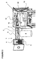
- Figure 2 is an isometric view of the coating system of Fig. 1 with some outer wall removed;
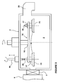
- Figure 3 is a schematic illustration of a planetary substrate holder with a magnetic latch according to the present invention.
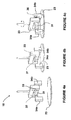
- FIGS. 4a to 4c are schematic illustrations of the basic principle of the magnetic latch according to the present invention.
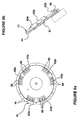
- Figure 5 is an isometric view of a magnetic latch according to the present invention.
- Figure 6a is a top view of a stator of the magnetic latch of Fig. 5;
- Figure 6b is a cross sectional view of the stator of Fig. 6a;
- Figure 7 is a top view of the magnetic latch of Fig. 5 in the unlatched position
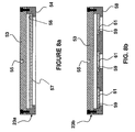
- Figures 8a to 8d are cross-section views of substrate holders according to the present invention.
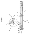
- Figure 9a is a cross-sectional side view of an alternative substrate holder
- Figure 9b are top view of the substrate holder of Fig. 9a.
- Figures 10 is a cross-sectional side view of an alternative substrate holders.
- the vapor deposition vacuum system e.g. Physical Vapor Deposition (PVD) or Chemical Vapor Deposition (CVD)
- a load lock chamber generally indicated at 1
- the gate valve 3 enables the pressure in the load lock chamber 1 to be brought to atmospheric pressure for loading and unloading of substrates or to be re-established to the pressure of the process chamber 2 for substrate transfer, independently of the pressure in the process chamber 2.
- the load lock chamber 1 includes a loading container 4 with a cassette elevator 5 therein, and a transfer channel 6 with a robotic arm 7 therein.
- the control mechanism for the robotic arm 7 is mounted in the cylindrical canister 8 extending from the transfer channel 6.
- a cathode 12, and a planetary substrate support 14 are mounted within the process chamber 2.
- the planetary substrate support 14 comprises a main cylindrical platform 16 rotatable about a first axis, with a plurality of, e.g. six, spindles 17 extending therefrom, each spindle 17 rotatable about its own axis, which are preferably parallel to the first axis, but may be at some other angle.
- each individual spindle 17 is also rotated to ensure even coating over all portions of each substrate.
- Each spindle 17 includes a magnetic latch 18 at the outer free end thereof for suspending a substrate over the cathode 12, which will be further described hereinafter
- At least one cathode 12, preferably low arcing cathodes, are mounted inside the process chamber 2.
- Extra cathodes 12 may be provided for backup in case of failure or in case the coating supply in one cathode 12 becomes exhausted.
- several different cathodes 12 can be provided to enable the deposition of different coatings consecutively without opening up the process chamber 2 to the atmosphere.
- minor adjustments can be made to the position of the cathode 12 by movement a mounting platform (not shown), manually or by remote control.
- the process chamber 2 is evacuated through pumping port 22, while process gases are supplied to the process chamber 2 via mass flow controllers (not shown).
- the planetary substrate support according to the present invention can be utilized with any other suitable coating system such as evaporative systems or CVD systems.
- the coating process can be enhanced by additional equipment such as shutters, masks, ion bombardment devices, advanced anode concepts, or plasma activation systems.
- magnetic latch according to the present invention can be utilized in other orientations such as coating down and coating sideways.
- Uncoated substrates mounted in substrate holders 23 are loaded onto the cassette elevator 5 with the gate valve 3 closed, thereby maintaining the pressure in the process chamber 2.
- the gate valve to the process chamber 2 opens and the robotic arm 7 transfers each substrate holder 23 through the transfer channel 6 and the open valve gate 3 to the process chamber 2 for mounting onto the spindles 17 with the help of the magnetic latches 18.
- FIG. 4a to 4c The basic principle behind the magnetic latch 18 is illustrated in Figure 4a to 4c, in which a permanent magnet 31 is disposed in an unlatched position (Figs 4a and 4b) or a latched position (Fig 4c).
- a magnetic circuit indicated by arrow 32
- the substrate holder 23 is brought in contact with the poles 34a and 34b providing an alternative magnetic circuit.
- the permanent magnet 31 is rotated into alignment with the poles 34a and 34b, thereby ensuring that the substrate holder 23 is magnetically attracted by the poles 34a and 34b.
- the permanent magnet 31 can remain fixed, while the bypass section 33 and the poles 34a and 34b are moved into and out of alignment therewith.
- a preferred embodiment of the magnetic latch 18, illustrated in Figures 5, 6a, 6b and 7, includes a cylindrical stator 41, with a cylindrical rotor 42 rotatable thereon.
- the stator 41 includes three sets of stator poles 43a and 43b fixed to a base 44 by a plurality of mechanical fasteners, e.g. hex bolts 46, ensuring good contact.
- the rotor 42 includes three radially extending permanent magnets 47 sandwiched between rotor poles 48a and 48b. The north and south poles of the permanent magnets extend along the long sides thereof adjacent to the rotor poles 48a and 48b, respectively.
- Each magnetic latch 18 includes an elongated actuator 49 extending down through the main platform 16 and each spindle 17 for rotating the rotors 42 between the latched position ( Figure 5) and the unlatched position ( Figure 7) from outside of the process chamber 2.
- the actuator 49 includes a tongue or other engageable feature on the upper end thereof for engagement by another mechanical device, e.g. a shaft 50 (Fig. 3), above the planetary substrate support.
- a shaft 50 Fig. 3
- a tapered pin 51 is provided extending from the center of the base 44.
- a single tapered pin 51 in the center of the base 44 provides an alignment feature, which ensures the proper alignment of the substrate holder 23 without dictating the exact angular orientation thereof.
- Tapered pins can be positioned at other positions around the circumference of the stator or other radial positions.
- the substrate holder 23a in Figure 8a, includes a base 53 fastened to an annular cover 54, which includes an annular shoulder 56 for supporting a single substrate 57.
- a cylindrical recess 55 is provided in the base 53 for receiving the tapered pin 51, thereby providing a mating alignment feature therefor.
- the base 53 if formed entirely or at least partially of a material that is attracted by the magnetic latch 18, e.g. a ferromagnetic material including one or more of iron, cobalt and nickel.
- the base 53 also provides a protective cover for the uncoated side of the substrate 57, thereby preventing unintentional and unwanted back coating.
- Substrate holder 23b (Fig 8b) includes a multi-disk annular cover 58 fastened to the base 53.
- the multi-disk cover 58 includes a plurality of annular shoulders 59 for supporting a plurality of smaller substrates 61.
- a multi-prism cover 63 is provided for mounting to the base 53, see Figure 8c.
- a ferromagnetic ring 71 for attraction to the stator 41, surrounds a substrate 72 (Fig 8d).
- An advantage to the ring 71 is the ability to coat the substrate 72 with the same or different coatings on opposite sides thereof without removing it from the ring 71. Moreover, the substrate 72 and ring 71 need not be removed from the process chamber 1, between coatings, e.g. simply flipped over by the robotic arm 7.
- a typical substrate would be a glass wafer 200 mm in diameter and 0.2 mm to 1.4 mm thick; however, other substrate forms are possible, e.g. up to 32 mm in thickness and a mass of up to 2 kg.
- a disposable cover 75 is mounted on a base 76, which, as above, is formed entirely or at least partially of a material that is attracted by the magnetic latch 18, e.g. a ferromagnetic material including one or more of iron, cobalt and nickel.
- the base 76 includes a cylindrical recess 77 for the tapered pin 51, and provides a protective cover for the uncoated side of the substrate, thereby preventing unintentional and unwanted back coating.
- the cover 75 includes one or more openings 78 for substrates, and defines a lip 79 extending around each opening 78. Each lip 79 holds an edge of a substrate in a slot 81 formed in an upper face of the base 76.
- the openings 78 are typically round, but could be any shape, e.g. square or oval, depending upon the shape of the substrate.
- the cover 75 also includes an annular intermediate region 82 to ensure the upper face of the base 76 is covered, thereby protected from stray coating material.
- An annular flange 83 extends perpendicularly from the intermediate region 82 adjacent to a sidewall of the base 76 to protect the sidewall of the base 76 from stray coating material.
- the outer free end 84 of the annular flange 83 is bent inwardly back around parallel with the rest of the annular flange 83 forming a clip for engaging a latching surface 88 the base 76.
- one or more separate clips could extend from the cover 75, perpendicular thereto, into engagement with a latching surface 88 on the base 82.
- the clips would be made of a resilient material, e.g. the same sheet metal as the cover 75, enabling the clips and the cover 75 to be manually released with relative ease, i.e. without the aid of tools.
- Various mechanical means can be provided to facilitate disengagement of the clips including levers, push buttons and rotating knobs extending therefrom.
- the latching surface 88 is disposed on a moveable wedge 89, which reciprocates towards the center, e.g. radially, of the base 76, i.e. towards cylindrical recess 77, when a sufficient force is applied thereto.
- a threaded fastener 91 extends through a slot 92 in the wedge 82 into the base 76 for guiding the wedge 89 during reciprocation.
- Springs 93 bias the wedges 89 outwardly into contact with the outer free end 84 (clip) of the annular flange 83, providing a set force, which must be manually overcome to release the cover 75 from the base 76.
- the embodiment illustrated in Figure 10 includes a modified stator portion 100 defined by an inverted cup shaped ferrous plate with a series of alternating north and south poles around a rim 101.
- the modified stator portion 100 is either mounted on the existing stator 41 or is a replacement therefore.
- a rotor 142 is provided along with actuator 149, as hereinbefore described.
- a disposable substrate holder 103 defines a substantially circular opening 104 into which a substrate is disposed.
- the substrate holder 103 is formed out of a first (base) ring 105a and a second (cover) ring 105b connected together at annular intermediate connecting regions 106a and 106b, respectively.
- the first and second rings 105a and 105b may be attached together with metal or plastic tape, folded over tabs, or other means.
- a preferred method is to "spot bond" the first and second rings 105a and 105b at an appropriate number of points near the periphery of the first and second rings 105a and 105b in the connecting regions 106a and 106b.
- Spot bonds using spot welding equipment and techniques with very low currents provide sufficient strength. Bonds range in a continuum from just melting the tin to make a "solder" spot to a full spot-weld of the parent steel.
- the current to the spot welding equipment can be adjusted, so that the first and second rings 105a and 105b are held together securely for handling, but can be easily and gently separated to remove the substrate without the need of heavy tools or excessive force.
- Each of the first and second rings 104a and 104b includes an annular lip 107a and 107b, respectively, extending inwardly from the connecting regions 106a and 106b, respectively, defining an annular slot 108 for receiving and clamping an edge of a substrate.
- Outer ends of the first and second rings 105a and 105b are bent perpendicularly to the connecting regions forming flanges 109a and 109b, respectively.
- the flange 109a extends along the side of the rim 101 for shielding the side of rim 101 from stray coating material and preventing stray coating material from traveling between the substrate holder 103 and the rim 101 onto the back surface of the substrate. Moreover, the flange 109a fits around the rim 100 to center the substrate holder 103 on the magnetic latch 18. The flange 109b extends outwardly from the connecting region 106b facilitating grasping, i.e. by machine or manually, for removal of the substrate holder 103 from the rim 101, and for protecting the base from stray coating material.
- the robotic arm 7 includes a n annular reception surface, which fits inside the flange 109b for receiving the substrate holder 103 when released from the magnetic latch 18.
- the first and second rings 105a and 105b are identical to each other; however, the first and second rings 105a and 105b can be different, e.g. non-symmetrical, to suite specific needs, e.g. special friction tabs can be formed into the lips 107a and/or 107b to support various substrates.
- one of the rings could be a flat ring, i.e. without the annular flange or the lip.
- the substrate holder 103 can be easily flipped over for coating of the opposite side of the substrate.
- First and second rings 105a and 105b which are intended to be flipped, must both be formed entirely or at least partially of a material that is attracted by the magnetic latch 18, e.g. a ferromagnetic material including one or more of iron, cobalt and nickel.
- the substrate holders utilize disposable covers 75, and 105b, which are fabricated from an inexpensive sheet metal stamping, which can be disposed of after one or two uses.
- the covers 75 and 105b hold the substrate securely and precisely relative to the bases 76 and 105a, respectively, during acceleration, vibration and temperature cycling.
- the covers 75 and 105b shield the bases 76 and 105a from stray coating flux, which would otherwise become deposited on the bases 76 and 105a causing damage to the substrates, if flaked off.
- the disposable covers 75 and 105b are ferromagnetic, so that they will be magnetically attracted by the stator 41 or the modified stator portion 100 via the base 76 and 105b, although cover 75 need not be ferromagnetic as it is mechanically attached to the base 76.
- the covers 75 and 105b should include surface materials or characteristics, which encourage adhesion of stray coating material.
- the covers 75 and 105b should be inexpensive, easily formable with enough resiliency to provide spring forces when appropriate, have a low vapor pressure at coating temperatures, and have minimal toxic waste issues.
- the covers 75 and 105b are up to 0.030 in. thick, but preferably up to 0.025 in. or even up to only 0.020 in. thick.
- the covers 75 and 105b are fabricated from electro-tinned steel (Tin Plate), which is relatively inexpensive, magnetic, and easily formed.
- the tin plating has a low vapor pressure (5.78 E-21 Pa @232.06 °C) at coating temperatures, which minimizes any material released therefrom from contaminating the substrates, and provides relatively good adhesion for most metals and metal oxides, whereby stray coating material will stick to the covers 75 and 105b rather than deflect onto the substrate.
- Te Plate electro-tinned steel
- tin plating has a low vapor pressure (5.78 E-21 Pa @232.06 °C) at coating temperatures, which minimizes any material released therefrom from contaminating the substrates, and provides relatively good adhesion for most metals and metal oxides, whereby stray coating material will stick to the covers 75 and 105b rather than deflect onto the substrate.
- tin 232 °C
- other sheet metals such as aluminum and stainless steel, can be used. Surface treatments may be necessary
Landscapes
- Chemical & Material Sciences (AREA)
- Engineering & Computer Science (AREA)
- Physics & Mathematics (AREA)
- Materials Engineering (AREA)
- Organic Chemistry (AREA)
- Metallurgy (AREA)
- Analytical Chemistry (AREA)
- Chemical Kinetics & Catalysis (AREA)
- Plasma & Fusion (AREA)
- General Chemical & Material Sciences (AREA)
- Crystallography & Structural Chemistry (AREA)
- Power Engineering (AREA)
- Electromagnetism (AREA)
- Mechanical Engineering (AREA)
- Physical Vapour Deposition (AREA)
- Container, Conveyance, Adherence, Positioning, Of Wafer (AREA)
- Audible-Bandwidth Dynamoelectric Transducers Other Than Pickups (AREA)
- Supporting Of Heads In Record-Carrier Devices (AREA)
- Chemical Vapour Deposition (AREA)
Abstract
Description
- The present invention claims priority from United States Patent Application No. 60/603,211 filed August 20, 2004, and is a continuation in part of United States Patent Application 10/968,642 filed October 19, 2004, which are incorporated herein by reference for all purposes.
- The present invention relates to a substrate holder for use in a vapor deposition system, and in particular to a partially disposable substrate holder for use with a magnetic latch, which suspends the substrate holder in a vacuum chamber of a physical vapor deposition (PVD) system or a chemical vapor deposition (CVD) system.
- Multi-layer precision coatings, such as those used small optical systems, are commonly produced in PVD or CVD systems. Many of these coatings are applied to substrates formed of thin flat disks, which are subsequently cut to size.
- The coating flux from a source in a PVD or a CVD system are relatively stable; however, they have a spatial distribution that can lead to deposited films with non-uniform thickness, if the substrates remain stationary. To improve uniformity, the geometrical relationship between the source and substrate must be selected appropriately. Good results have been observed when the substrate is rotated about an axis perpendicular to the plane of the surface to be coated, and in particular when multiple substrates have been mounted on multiple spindles in a planetary configuration.
- For repeatable thickness control and low defect count the substrate holders must locate the substrate very precisely relative to the other motion elements, and must hold the substrate securely to prevent sliding motion, which could generate particulate contamination under acceleration or temperature changes. Furthermore, the surface of the tooling, (the jig lip) which supports the substrate, must be polished, and must be very thin to prevent shadowing of coating flux arriving at non-normal incidence. The rear surface of the substrate must be shielded to prevent stray coating material from becoming deposited thereon.
- To meet these demanding requirements substrate holders for high volume production are typically made of stainless, or even hardened stainless, steel, which is relatively expensive and difficult to maintain. Surfaces adjacent to the substrate are exposed to the same coating flux as the substrate, e.g. multi-layers of hard metal oxides. Unfortunately, the coating on the substrate holders builds up with each coating run and, if not removed, will flake into abrasive particles, which can cause damage to subsequent products. Cleaning the substrate holders usually requires grit blasting or very aggressive chemical etching, which must be repeated every few coating runs or, if very few defects are required, after each coating run. Even hardened steel substrate holders wear out rapidly, resulting in that the substrate holders and the maintenance thereof are a significant cost in the coating process, and a major source of particulate generated defects.
- Conventional planetary gear coating systems, such as the one disclosed in United States Patent No. 5,106,346, issued April 21, 1992 to Stefan Locher et al, includes a large rotating platform with several individual spindles (planets) rotatable thereon disposed within a sealed vacuum chamber. Unfortunately, each substrate holder must be connected to a mounting flange on each spindle using mechanical fasteners, e.g. bolts, requiring manual replacement. Not only do these mechanical systems require extra manual labor, they are more susceptible to misalignment caused by changes in temperature and pressure.
- In order to isolate as much of the bearing and gear structure as possible from the vacuum chamber, Hurwitt et al disclosed a planetary gear coating system in United States Patent No. 5,795,448 issued August 18, 1998, which includes a magnetic link in the shaft of each spindle. The substrate holders are not suspended over the cathodes, and still require mechanical fasteners for attachment to the mounting flanges of the spindles.
- The coating system, disclosed in United States Patent No. 6,464,825 issued October 15, 2002 to Shinozaki, includes a robotic arm traveling between a pressurized loading/unloading chamber and the main vacuum chamber to minimize the amount dust entering the main vacuum chamber. The Shinozaki system also includes a magnetic rotational drive and a magnetic levitating member to minimize particulate generation caused by interacting mechanical elements. However, Shinozaki discloses a single rotating platform with a complicated levitating platform and electro-magnets that totally surround the substrate holder. Unfortunately, this approach would be impossible to implement in a planetary gear coating system, as it is very difficult to deliver power separately to individual rotating substrate holders in a planetary system, while operating in a vacuum and at elevated temperatures.
- An object of the present invention is to overcome the shortcomings of the prior art by providing a substrate holder with a disposable cover, which is easily removable from the base, and can be easily dismantled to remove the substrate therefrom.
- Accordingly, the present invention relates to a substrate support for mounting in a process chamber of a coating system, comprising:
- at least one spindle rotatable about respective spindle axes;
- a latch on an end of each spindle including a mounting surface; and
- a releasable substrate holder for mounting on the mounting surface of said latch, said substrate holder including a base and a cover mounted on an end face of the base for supporting a substrate;
- wherein the cover includes an opening to expose the substrate, a lip surrounding the opening for holding an edge of the substrate against the base, and a protective region covering the end face of the base for protecting the base from stray coating material;
- wherein the cover is made of a sheet metal; and
- wherein the cover is releasably attached to said base for removal therefrom
- The invention will be described in greater detail with reference to the accompanying drawings which represent preferred embodiments thereof, wherein:
- Figure 1 is an isometric view of the coating system according to the present invention;
- Figure 2 is an isometric view of the coating system of Fig. 1 with some outer wall removed;
- Figure 3 is a schematic illustration of a planetary substrate holder with a magnetic latch according to the present invention;
- Figures 4a to 4c are schematic illustrations of the basic principle of the magnetic latch according to the present invention;
- Figure 5 is an isometric view of a magnetic latch according to the present invention;
- Figure 6a is a top view of a stator of the magnetic latch of Fig. 5;
- Figure 6b is a cross sectional view of the stator of Fig. 6a;
- Figure 7 is a top view of the magnetic latch of Fig. 5 in the unlatched position;
- Figures 8a to 8d are cross-section views of substrate holders according to the present invention;
- Figure 9a is a cross-sectional side view of an alternative substrate holder;
- Figure 9b are top view of the substrate holder of Fig. 9a; and
- Figures 10 is a cross-sectional side view of an alternative substrate holders.
- With reference to Figures 1 to 3, the vapor deposition vacuum system, e.g. Physical Vapor Deposition (PVD) or Chemical Vapor Deposition (CVD), according to the present invention includes a load lock chamber, generally indicated at 1, and a
process chamber 2 with agate valve 3 therebetween. Thegate valve 3 enables the pressure in theload lock chamber 1 to be brought to atmospheric pressure for loading and unloading of substrates or to be re-established to the pressure of theprocess chamber 2 for substrate transfer, independently of the pressure in theprocess chamber 2. Theload lock chamber 1 includes aloading container 4 with acassette elevator 5 therein, and atransfer channel 6 with arobotic arm 7 therein. The control mechanism for therobotic arm 7 is mounted in thecylindrical canister 8 extending from thetransfer channel 6. - A
cathode 12, and aplanetary substrate support 14 are mounted within theprocess chamber 2. Theplanetary substrate support 14 comprises a maincylindrical platform 16 rotatable about a first axis, with a plurality of, e.g. six,spindles 17 extending therefrom, eachspindle 17 rotatable about its own axis, which are preferably parallel to the first axis, but may be at some other angle. In use, as themain platform 16 is rotated, eachindividual spindle 17 is also rotated to ensure even coating over all portions of each substrate. Eachspindle 17 includes amagnetic latch 18 at the outer free end thereof for suspending a substrate over thecathode 12, which will be further described hereinafter - At least one
cathode 12, preferably low arcing cathodes, are mounted inside theprocess chamber 2.Extra cathodes 12 may be provided for backup in case of failure or in case the coating supply in onecathode 12 becomes exhausted. Alternatively, severaldifferent cathodes 12 can be provided to enable the deposition of different coatings consecutively without opening up theprocess chamber 2 to the atmosphere. Preferably, minor adjustments can be made to the position of thecathode 12 by movement a mounting platform (not shown), manually or by remote control. - The
process chamber 2 is evacuated through pumpingport 22, while process gases are supplied to theprocess chamber 2 via mass flow controllers (not shown). - While sputter deposition vacuum systems have been described herein, the planetary substrate support according to the present invention can be utilized with any other suitable coating system such as evaporative systems or CVD systems. The coating process can be enhanced by additional equipment such as shutters, masks, ion bombardment devices, advanced anode concepts, or plasma activation systems.
- While the coating system is shown in a sputter up configuration herein, magnetic latch according to the present invention can be utilized in other orientations such as coating down and coating sideways.
- Uncoated substrates mounted in
substrate holders 23 are loaded onto thecassette elevator 5 with thegate valve 3 closed, thereby maintaining the pressure in theprocess chamber 2. When theload lock chamber 1 is evacuated, the gate valve to theprocess chamber 2 opens and therobotic arm 7 transfers eachsubstrate holder 23 through thetransfer channel 6 and theopen valve gate 3 to theprocess chamber 2 for mounting onto thespindles 17 with the help of themagnetic latches 18. - The basic principle behind the
magnetic latch 18 is illustrated in Figure 4a to 4c, in which apermanent magnet 31 is disposed in an unlatched position (Figs 4a and 4b) or a latched position (Fig 4c). In Figure 4a, a magnetic circuit, indicated byarrow 32, is completed through abypass section 33 leavingpoles substrate holder 23 is brought in contact with thepoles arrow 36 in Fig. 4c, thepermanent magnet 31 is rotated into alignment with thepoles substrate holder 23 is magnetically attracted by thepoles permanent magnet 31 can remain fixed, while thebypass section 33 and thepoles - A preferred embodiment of the
magnetic latch 18, illustrated in Figures 5, 6a, 6b and 7, includes acylindrical stator 41, with acylindrical rotor 42 rotatable thereon. Thestator 41 includes three sets ofstator poles base 44 by a plurality of mechanical fasteners,e.g. hex bolts 46, ensuring good contact. Therotor 42 includes three radially extendingpermanent magnets 47 sandwiched betweenrotor poles rotor poles magnetic latch 18 includes anelongated actuator 49 extending down through themain platform 16 and eachspindle 17 for rotating therotors 42 between the latched position (Figure 5) and the unlatched position (Figure 7) from outside of theprocess chamber 2. Theactuator 49 includes a tongue or other engageable feature on the upper end thereof for engagement by another mechanical device, e.g. a shaft 50 (Fig. 3), above the planetary substrate support. In the unlatched position both of therotor poles stator poles 43b, thereby shorting thepermanent magnet 47, breaking the magnetic circuit through thestator 41, thereby unmagnetizing thestator 41 and releasing thesubstrate holder 23. - To facilitate alignment of the
substrate holder 23 with thestator 41, a taperedpin 51 is provided extending from the center of thebase 44. A single taperedpin 51 in the center of thebase 44 provides an alignment feature, which ensures the proper alignment of thesubstrate holder 23 without dictating the exact angular orientation thereof. Tapered pins can be positioned at other positions around the circumference of the stator or other radial positions. - Examples of
substrate holders 23 are illustrated in Figures 8a to 8d. Thesubstrate holder 23a, in Figure 8a, includes a base 53 fastened to anannular cover 54, which includes anannular shoulder 56 for supporting asingle substrate 57. Acylindrical recess 55 is provided in thebase 53 for receiving the taperedpin 51, thereby providing a mating alignment feature therefor. The base 53 if formed entirely or at least partially of a material that is attracted by themagnetic latch 18, e.g. a ferromagnetic material including one or more of iron, cobalt and nickel. The base 53 also provides a protective cover for the uncoated side of thesubstrate 57, thereby preventing unintentional and unwanted back coating.Substrate holder 23b (Fig 8b) includes a multi-diskannular cover 58 fastened to thebase 53. Themulti-disk cover 58 includes a plurality ofannular shoulders 59 for supporting a plurality ofsmaller substrates 61. For odd shaped substrates, such asprisms 62, amulti-prism cover 63 is provided for mounting to thebase 53, see Figure 8c. - As an alternative to the
base 53, aferromagnetic ring 71, for attraction to thestator 41, surrounds a substrate 72 (Fig 8d). An advantage to thering 71 is the ability to coat thesubstrate 72 with the same or different coatings on opposite sides thereof without removing it from thering 71. Moreover, thesubstrate 72 andring 71 need not be removed from theprocess chamber 1, between coatings, e.g. simply flipped over by therobotic arm 7. - A typical substrate would be a glass wafer 200 mm in diameter and 0.2 mm to 1.4 mm thick; however, other substrate forms are possible, e.g. up to 32 mm in thickness and a mass of up to 2 kg.
- With reference to Figures 9a and 9b, a
disposable cover 75 is mounted on abase 76, which, as above, is formed entirely or at least partially of a material that is attracted by themagnetic latch 18, e.g. a ferromagnetic material including one or more of iron, cobalt and nickel. Thebase 76 includes acylindrical recess 77 for the taperedpin 51, and provides a protective cover for the uncoated side of the substrate, thereby preventing unintentional and unwanted back coating. Thecover 75 includes one ormore openings 78 for substrates, and defines alip 79 extending around eachopening 78. Eachlip 79 holds an edge of a substrate in aslot 81 formed in an upper face of thebase 76. Theopenings 78 are typically round, but could be any shape, e.g. square or oval, depending upon the shape of the substrate. Thecover 75 also includes an annularintermediate region 82 to ensure the upper face of thebase 76 is covered, thereby protected from stray coating material. Anannular flange 83 extends perpendicularly from theintermediate region 82 adjacent to a sidewall of the base 76 to protect the sidewall of the base 76 from stray coating material. The outerfree end 84 of theannular flange 83 is bent inwardly back around parallel with the rest of theannular flange 83 forming a clip for engaging a latchingsurface 88 thebase 76. Alternatively, one or more separate clips could extend from thecover 75, perpendicular thereto, into engagement with a latchingsurface 88 on thebase 82. Preferably, the clips would be made of a resilient material, e.g. the same sheet metal as thecover 75, enabling the clips and thecover 75 to be manually released with relative ease, i.e. without the aid of tools. Various mechanical means can be provided to facilitate disengagement of the clips including levers, push buttons and rotating knobs extending therefrom. - However, in the illustrated embodiment to facilitate removal of the
cover 75 from thebase 76, the latchingsurface 88 is disposed on amoveable wedge 89, which reciprocates towards the center, e.g. radially, of thebase 76, i.e. towardscylindrical recess 77, when a sufficient force is applied thereto. A threadedfastener 91 extends through aslot 92 in thewedge 82 into thebase 76 for guiding thewedge 89 during reciprocation.Springs 93 bias thewedges 89 outwardly into contact with the outer free end 84 (clip) of theannular flange 83, providing a set force, which must be manually overcome to release thecover 75 from thebase 76. - The embodiment illustrated in Figure 10, includes a modified
stator portion 100 defined by an inverted cup shaped ferrous plate with a series of alternating north and south poles around arim 101. The modifiedstator portion 100 is either mounted on the existingstator 41 or is a replacement therefore. Arotor 142 is provided along withactuator 149, as hereinbefore described. Adisposable substrate holder 103 defines a substantiallycircular opening 104 into which a substrate is disposed. Thesubstrate holder 103 is formed out of a first (base)ring 105a and a second (cover)ring 105b connected together at annular intermediate connectingregions - The first and
second rings second rings second rings regions second rings - Each of the first and second rings 104a and 104b includes an
annular lip regions annular slot 108 for receiving and clamping an edge of a substrate. Outer ends of the first andsecond rings regions forming flanges regions rim 101, theflange 109a extends along the side of therim 101 for shielding the side ofrim 101 from stray coating material and preventing stray coating material from traveling between thesubstrate holder 103 and therim 101 onto the back surface of the substrate. Moreover, theflange 109a fits around therim 100 to center thesubstrate holder 103 on themagnetic latch 18. Theflange 109b extends outwardly from the connectingregion 106b facilitating grasping, i.e. by machine or manually, for removal of thesubstrate holder 103 from therim 101, and for protecting the base from stray coating material. In a preferred embodiment therobotic arm 7 includes a n annular reception surface, which fits inside theflange 109b for receiving thesubstrate holder 103 when released from themagnetic latch 18. - To minimize costs and facilitate storage, the first and
second rings second rings lips 107a and/or 107b to support various substrates. Furthermore, one of the rings could be a flat ring, i.e. without the annular flange or the lip. However, if the first andsecond rings substrate holder 103 can be easily flipped over for coating of the opposite side of the substrate. First andsecond rings magnetic latch 18, e.g. a ferromagnetic material including one or more of iron, cobalt and nickel. - The substrate holders, illustrated in Figures 9 and 10, utilize
disposable covers covers bases covers bases bases - Ideally the disposable covers 75 and 105b are ferromagnetic, so that they will be magnetically attracted by the
stator 41 or the modifiedstator portion 100 via thebase cover 75 need not be ferromagnetic as it is mechanically attached to thebase 76. Moreover, thecovers covers covers covers covers
Claims (20)
- A substrate support for mounting in a process chamber of a coating system, comprising:at least one spindle rotatable about respective spindle axes;a latch on an end of each spindle including a mounting surface; anda releasable substrate holder for mounting on the mounting surface of said latch, said substrate holder including a base and a cover mounted on an end face of the base for supporting a substrate;wherein the cover includes an opening to expose the substrate, a lip surrounding the opening for holding an edge of the substrate against the base, and a protective region covering the end face of the base for protecting the base from stray coating material;wherein the cover is made of a sheet metal; andwherein the cover is releasably attached to said base for removal therefrom.
- The substrate support according to claim 1, wherein the cover further comprises an annular flange extending substantially perpendicularly from said intermediate region for protecting the base from stray coating material.
- The substrate support according to claim 2, wherein the annular flange extends adjacent to a side wall of said base to protect the side wall from stray coating material.
- The substrate support according to claim 3, further comprising a clip extending from said annular flange for releasably attaching said cover to said base.
- The substrate support according to claim 4, further comprising a reciprocating latching surface on said base moveable between a first position engaging said clamp and a second position in which the clamp is released.
- The substrate support according to claim 5, wherein said latching surface is spring biased into said first position.
- The substrate support according to claim 1, wherein the annular flange extends outwardly away from said cover for facilitating grasping of the substrate holder.
- The substrate support according to claim 7, wherein the base comprises a lip, an intermediate region, and an annular flange opposite the lip, the intermediate region and the annular flange of the cover, respectively; wherein the lip of the base and the lip of the cover form an annular slot for receiving the substrate; and wherein the annular flange of the base extends adjacent to a side wall of said latch to protect the side wall from stray coating material.
- The substrate support according to claim 8, wherein the base and the cover have substantially the same structure enabling the substrate holder to be flipped over for coating both sides of the substrate.
- The substrate support according to claim 9, wherein the intermediate region of the base is spot bonded to the intermediate region of the cover enabling manual disengagement thereof.
- The substrate support according to claim 10, wherein each latch is a magnetic latch for attracting the base to the spindle.
- The substrate support according to claim 11, wherein the magnetic latch comprises an annular rim for attracting the intermediate region of the base; wherein the annular flange of the base extends adjacent a side wall of said annular rim to protect the side wall of said annular rim from stray coating material.
- The substrate support according to claim 1, wherein each latch is a magnetic latch for attracting the base to the spindle.
- The substrate support according to claim 13, wherein each magnetic latch includes a first section, and a second section movable relative to the first section between a first position in which the permanent magnet magnetizes the mounting surface for attracting a substrate holder, and a second position in which the mounting surface is unmagnetized.
- The substrate support according to claim 14, wherein each of the first sections comprises a stator including the mounting surface, and poles for aligning with the permanent magnet; and
wherein each of the second sections comprises a rotor, including the permanent magnet for rotation between the first position in which the permanent magnet is aligned with the poles of the stator, and the second position in which the permanent magnet is not aligned with the poles of the stator, thereby making the stator unmagnetized. - The substrate support according to claim 15, wherein each magnetic latch further comprises an actuator extending through the spindle for rotating each rotor.
- The substrate support according to claim 15, wherein each rotor includes a plurality of permanent magnets; and each stator includes a plurality of poles for aligning with the plurality of permanent magnets.
- The substrate support according to claim 17, wherein each rotor includes a rotor pole on each side of each permanent magnet for aligning with respective stator poles, which forms a magnetic circuit through the mounting surface when in the first position, and for engaging a single stator pole, which shorts the permanent magnet when in the second position.
- The substrate support according to claim 1, wherein the cover is comprised of a sheet metal stamping of tin-plated steel to encourage adhesion of stray coating material thereto.
- The substrate support according to claim 1, wherein the cover is up to 0.015 inches thick.
Applications Claiming Priority (2)
| Application Number | Priority Date | Filing Date | Title |
|---|---|---|---|
| US60321104P | 2004-08-20 | 2004-08-20 | |
| US10/968,642 US7785456B2 (en) | 2004-10-19 | 2004-10-19 | Magnetic latch for a vapour deposition system |
Publications (3)
| Publication Number | Publication Date |
|---|---|
| EP1630261A2 true EP1630261A2 (en) | 2006-03-01 |
| EP1630261A3 EP1630261A3 (en) | 2008-12-10 |
| EP1630261B1 EP1630261B1 (en) | 2012-09-19 |
Family
ID=35457340
Family Applications (2)
| Application Number | Title | Priority Date | Filing Date |
|---|---|---|---|
| EP05255001A Expired - Lifetime EP1630260B1 (en) | 2004-08-20 | 2005-08-11 | Magnetic latch for a vapour deposition system |
| EP05255095A Expired - Lifetime EP1630261B1 (en) | 2004-08-20 | 2005-08-17 | Substrate holder for a vapour deposition system |
Family Applications Before (1)
| Application Number | Title | Priority Date | Filing Date |
|---|---|---|---|
| EP05255001A Expired - Lifetime EP1630260B1 (en) | 2004-08-20 | 2005-08-11 | Magnetic latch for a vapour deposition system |
Country Status (8)
| Country | Link |
|---|---|
| US (1) | US7790004B2 (en) |
| EP (2) | EP1630260B1 (en) |
| JP (2) | JP4907125B2 (en) |
| CN (2) | CN1737191B (en) |
| AT (1) | ATE516390T1 (en) |
| DK (1) | DK1630260T3 (en) |
| PL (1) | PL1630260T3 (en) |
| PT (1) | PT1630260E (en) |
Cited By (8)
| Publication number | Priority date | Publication date | Assignee | Title |
|---|---|---|---|---|
| JP2006057185A (en) * | 2004-08-20 | 2006-03-02 | Jds Uniphase Corp | Substrate holder for vapor deposition system |
| WO2013082488A3 (en) * | 2011-11-30 | 2013-08-22 | Corning Incorporated | Optical coating method, apparatus and product |
| WO2014055134A1 (en) * | 2012-10-04 | 2014-04-10 | Corning Incorporated | Optical coating method, appartus and product |
| US9831007B2 (en) | 2014-04-28 | 2017-11-28 | Agfa Healthcare Nv | Radiographic flat panel detector having a ferromagnetic layer and the method of production thereof |
| US9957609B2 (en) | 2011-11-30 | 2018-05-01 | Corning Incorporated | Process for making of glass articles with optical and easy-to-clean coatings |
| US10077207B2 (en) | 2011-11-30 | 2018-09-18 | Corning Incorporated | Optical coating method, apparatus and product |
| EP3787804A4 (en) * | 2018-05-04 | 2022-02-09 | Jiangsu Favored Nanotechnology Co., Ltd. | Nano-coating protection method for electrical devices |
| US20230146946A1 (en) * | 2019-09-16 | 2023-05-11 | Halliburton Energy Services, Inc. | Customized Thin Film Optical Element Fabrication System and Method |
Families Citing this family (29)
| Publication number | Priority date | Publication date | Assignee | Title |
|---|---|---|---|---|
| US7954219B2 (en) * | 2004-08-20 | 2011-06-07 | Jds Uniphase Corporation | Substrate holder assembly device |
| JP2006199998A (en) * | 2005-01-20 | 2006-08-03 | Seiko Epson Corp | Film forming apparatus and film forming method |
| DE102006032959B3 (en) * | 2006-07-17 | 2007-12-27 | JOH. WINKLHOFER & SÖHNE GMBH & Co. KG | Workpiece support for a vacuum coating installation comprises a support body having radially protruding magnetic holding bodies with a holding surface for workpieces to be coated |
| DE102006041137B4 (en) * | 2006-09-01 | 2015-02-12 | Carl Zeiss Vision Gmbh | Apparatus for turning an article in a vacuum coating machine, method of turning an article in a vacuum coating machine, and use thereof |
| JP4941197B2 (en) * | 2007-09-25 | 2012-05-30 | 三菱電機株式会社 | Semiconductor device deposition holder and deposition apparatus |
| US7853475B2 (en) * | 2007-11-09 | 2010-12-14 | Motorola Mobility, Inc. | Intelligent advertising based on mobile content |
| US8563407B2 (en) * | 2009-04-08 | 2013-10-22 | Varian Semiconductor Equipment Associates, Inc. | Dual sided workpiece handling |
| US10550474B1 (en) | 2010-02-26 | 2020-02-04 | Quantum Innovations, Inc. | Vapor deposition system |
| US10808319B1 (en) | 2010-02-26 | 2020-10-20 | Quantum Innovations, Inc. | System and method for vapor deposition of substrates with circular substrate frame that rotates in a planetary motion and curved lens support arms |
| JP5619666B2 (en) * | 2010-04-16 | 2014-11-05 | ジェイディーエス ユニフェイズ コーポレーションJDS Uniphase Corporation | Ring cathode for use in magnetron sputtering devices |
| CN101956177B (en) * | 2010-10-21 | 2012-08-22 | 湖南玉丰真空科学技术有限公司 | Rotary bin for vacuum continuous coating production line |
| CN101974733B (en) * | 2010-10-21 | 2012-07-04 | 湖南玉丰真空科学技术有限公司 | Rotary mechanism for vacuum continuous coating production line |
| US9109289B2 (en) | 2011-06-27 | 2015-08-18 | United Technologies Corporation | Manipulator for coating application |
| US9659706B2 (en) * | 2011-09-22 | 2017-05-23 | The Trustees Of Dartmouth College | Methods for making radially anisotropic thin-film magnetic torroidal cores |
| US9144816B2 (en) * | 2011-12-16 | 2015-09-29 | Ppg Industries Ohio, Inc. | Carrier systems for coating panels |
| WO2013094707A1 (en) * | 2011-12-22 | 2013-06-27 | 株式会社ブイ・テクノロジー | Deposition apparatus |
| JP5994088B2 (en) * | 2011-12-22 | 2016-09-21 | 株式会社ブイ・テクノロジー | Vapor deposition equipment |
| JP5994089B2 (en) * | 2011-12-29 | 2016-09-21 | 株式会社ブイ・テクノロジー | Vapor deposition equipment |
| MX373826B (en) * | 2012-03-20 | 2020-03-24 | Quantum Innovations Inc | VAPOR DEPOSITION SYSTEM AND METHOD. |
| EP2650135A1 (en) * | 2012-04-12 | 2013-10-16 | KBA-NotaSys SA | Intaglio printing plate coating apparatus |
| JP6244103B2 (en) | 2012-05-04 | 2017-12-06 | ヴァイアヴィ・ソリューションズ・インコーポレイテッドViavi Solutions Inc. | Method and reactive sputter deposition system for reactive sputter deposition |
| CN103074610A (en) * | 2012-08-28 | 2013-05-01 | 光达光电设备科技(嘉兴)有限公司 | Substrate supporting structure and reaction chamber containing the same |
| CN105143500B (en) * | 2012-10-04 | 2017-10-10 | 康宁股份有限公司 | Optics painting method, equipment and product |
| CN104342758B (en) * | 2013-07-24 | 2017-07-21 | 北京北方微电子基地设备工艺研究中心有限责任公司 | pressure ring and plasma processing device |
| CN104329332B (en) * | 2014-08-28 | 2020-04-03 | 北京可以科技有限公司 | Rotary connection unit and modular robot monomer |
| EP3279364B1 (en) * | 2016-08-03 | 2021-10-06 | IHI Hauzer Techno Coating B.V. | Apparatus for coating substrates |
| RU2625698C1 (en) * | 2016-08-29 | 2017-07-18 | Федеральное государственное унитарное предприятие "Всероссийский научно-исследовательский институт авиационных материалов" (ФГУП "ВИАМ") | Method of application of protective coatings and device for its implementation |
| CN106521446B (en) * | 2016-10-09 | 2019-01-11 | 深圳市万普拉斯科技有限公司 | Vacuum coating method and vacuum coating jig |
| CN106637140B (en) * | 2016-11-30 | 2018-08-10 | 江苏菲沃泰纳米科技有限公司 | A kind of nano-coating equipment planet gyration frame equipments for goods |
Citations (3)
| Publication number | Priority date | Publication date | Assignee | Title |
|---|---|---|---|---|
| US5106346A (en) | 1990-08-14 | 1992-04-21 | Leybold Aktiengesellschaft | Planetary gear system with a set of gears, particularly for devices for coating substrates |
| US5795448A (en) | 1995-12-08 | 1998-08-18 | Sony Corporation | Magnetic device for rotating a substrate |
| US6464825B1 (en) | 1999-06-15 | 2002-10-15 | Ebara Corporation | Substrate processing apparatus including a magnetically levitated and rotated substrate holder |
Family Cites Families (47)
| Publication number | Priority date | Publication date | Assignee | Title |
|---|---|---|---|---|
| US14368A (en) * | 1856-03-04 | Method | ||
| US189228A (en) * | 1877-04-03 | Improvement in spark-arresters | ||
| FR1534917A (en) * | 1967-06-22 | 1968-08-02 | Alcatel Sa | Improvements in obtaining deposits by cathodic sputtering |
| US3858547A (en) * | 1973-12-14 | 1975-01-07 | Nils H Bergfelt | Coating machine having an adjustable rotation system |
| CH599982A5 (en) * | 1975-09-02 | 1978-06-15 | Balzers Patent Beteilig Ag | |
| US4226208A (en) * | 1977-08-04 | 1980-10-07 | Canon Kabushiki Kaisha | Vapor deposition apparatus |
| US4222345A (en) * | 1978-11-30 | 1980-09-16 | Optical Coating Laboratory, Inc. | Vacuum coating apparatus with rotary motion assembly |
| US4250009A (en) * | 1979-05-18 | 1981-02-10 | International Business Machines Corporation | Energetic particle beam deposition system |
| JPS5914640A (en) * | 1982-07-15 | 1984-01-25 | Sanyo Electric Co Ltd | High frequency sputtering method |
| US4485759A (en) * | 1983-01-19 | 1984-12-04 | Multi-Arc Vacuum Systems Inc. | Planetary substrate support apparatus for vapor vacuum deposition coating |
| JPS6110239A (en) | 1984-06-25 | 1986-01-17 | Nec Kansai Ltd | Semiconductor manufacturing equipment |
| JPS61157682A (en) * | 1984-12-28 | 1986-07-17 | Toa Nenryo Kogyo Kk | Holding method of mask for vapor deposition |
| JPH0348204Y2 (en) * | 1985-03-20 | 1991-10-15 | ||
| JPS6394424A (en) * | 1986-10-08 | 1988-04-25 | Yamaha Corp | Production of thin film magnetic head |
| JPS63257942A (en) * | 1987-04-15 | 1988-10-25 | Oki Electric Ind Co Ltd | Production of medium for magneto-optical recording |
| JPH084105B2 (en) * | 1987-06-19 | 1996-01-17 | 株式会社エンヤシステム | Wafer bonding method |
| JPH01310512A (en) * | 1988-06-08 | 1989-12-14 | Seiko Epson Corp | magnetic stand |
| JPH0748667Y2 (en) * | 1989-05-31 | 1995-11-08 | 株式会社島津製作所 | Substrate rotation mechanism of film forming equipment |
| US4988424A (en) * | 1989-06-07 | 1991-01-29 | Ppg Industries, Inc. | Mask and method for making gradient sputtered coatings |
| JP2959023B2 (en) * | 1990-02-23 | 1999-10-06 | 日本電気株式会社 | Ion beam sputtering equipment |
| JPH0418655A (en) * | 1990-05-11 | 1992-01-22 | Mitsubishi Electric Corp | Data processor |
| RU2008501C1 (en) | 1990-10-09 | 1994-02-28 | Валерий Андреевич Попов | Air cleaner for internal combustion engine |
| JP2981682B2 (en) * | 1990-11-30 | 1999-11-22 | 新明和工業株式会社 | Vacuum evaporation system of continuous film formation method |
| JP3070158B2 (en) * | 1991-07-04 | 2000-07-24 | 日新電機株式会社 | Susceptor rotation support structure for thin film vapor phase growth equipment |
| US5232569A (en) * | 1992-03-09 | 1993-08-03 | Tulip Memory Systems, Inc. | Circularly symmetric, large-area, high-deposition-rate sputtering apparatus for the coating of disk substrates |
| US5444217A (en) * | 1993-01-21 | 1995-08-22 | Moore Epitaxial Inc. | Rapid thermal processing apparatus for processing semiconductor wafers |
| JPH0960310A (en) * | 1995-08-21 | 1997-03-04 | Nippon Pneumatic Mfg Co Ltd | Hydraulic breaker |
| US6054029A (en) * | 1996-02-23 | 2000-04-25 | Singulus Technologies Gmbh | Device for gripping, holdings and/or transporting substrates |
| JPH09256159A (en) * | 1996-03-15 | 1997-09-30 | Sony Corp | Work moving device and work moving method |
| JP2839003B2 (en) * | 1996-04-05 | 1998-12-16 | 日本電気株式会社 | Vacuum deposition equipment |
| DE19614600C1 (en) * | 1996-04-13 | 1997-04-24 | Singulus Technologies Gmbh | Device for masking central and outer areas of substrate to be sputter coated |
| US5820329A (en) * | 1997-04-10 | 1998-10-13 | Tokyo Electron Limited | Vacuum processing apparatus with low particle generating wafer clamp |
| US6575737B1 (en) * | 1997-06-04 | 2003-06-10 | Applied Materials, Inc. | Method and apparatus for improved substrate handling |
| JPH11131212A (en) * | 1997-10-28 | 1999-05-18 | Canon Inc | Single-wafer sputtering apparatus, single-wafer sputtering method, and sputtered film |
| US6096404A (en) * | 1997-12-05 | 2000-08-01 | Applied Materials, Inc. | Full face mask for capacitance-voltage measurements |
| US6030513A (en) * | 1997-12-05 | 2000-02-29 | Applied Materials, Inc. | Full face mask for capacitance-voltage measurements |
| DE19814834A1 (en) * | 1998-04-02 | 1999-10-07 | Leybold Systems Gmbh | Gripping and holding apparatus for a flat substrate e.g. a compact disk substrate during vacuum thin film coating |
| US6264804B1 (en) * | 2000-04-12 | 2001-07-24 | Ske Technology Corp. | System and method for handling and masking a substrate in a sputter deposition system |
| WO2002019379A1 (en) | 2000-08-28 | 2002-03-07 | Institute For Plasma Research | Device and process for producing dc glow discharge |
| JP2001203231A (en) * | 2000-12-11 | 2001-07-27 | Sony Corp | Manufacturing method of flip chip solder bump |
| DE10150809B4 (en) * | 2001-10-15 | 2005-06-16 | Steag Hamatech Ag | substrate holder |
| US6800833B2 (en) * | 2002-03-29 | 2004-10-05 | Mariusch Gregor | Electromagnetically levitated substrate support |
| US7601248B2 (en) | 2002-06-21 | 2009-10-13 | Ebara Corporation | Substrate holder and plating apparatus |
| JP3827627B2 (en) * | 2002-08-13 | 2006-09-27 | 株式会社荏原製作所 | Plating apparatus and plating method |
| JP2004259919A (en) * | 2003-02-26 | 2004-09-16 | Ulvac Japan Ltd | Vacuum transfer device and vacuum processing device |
| US20050189228A1 (en) | 2004-02-27 | 2005-09-01 | Taiwan Semiconductor Manufacturing Co., Ltd. | Electroplating apparatus |
| DK1630260T3 (en) * | 2004-08-20 | 2011-10-31 | Jds Uniphase Inc | Magnetic holding mechanism for a vapor deposition system |
-
2005
- 2005-08-11 DK DK05255001.9T patent/DK1630260T3/en active
- 2005-08-11 EP EP05255001A patent/EP1630260B1/en not_active Expired - Lifetime
- 2005-08-11 AT AT05255001T patent/ATE516390T1/en active
- 2005-08-11 PT PT05255001T patent/PT1630260E/en unknown
- 2005-08-11 PL PL05255001T patent/PL1630260T3/en unknown
- 2005-08-17 EP EP05255095A patent/EP1630261B1/en not_active Expired - Lifetime
- 2005-08-17 US US11/205,513 patent/US7790004B2/en active Active
- 2005-08-19 JP JP2005238271A patent/JP4907125B2/en not_active Expired - Fee Related
- 2005-08-19 JP JP2005238257A patent/JP4790344B2/en not_active Expired - Fee Related
- 2005-08-22 CN CN2005100928247A patent/CN1737191B/en not_active Expired - Fee Related
- 2005-08-22 CN CN2005100928266A patent/CN1737192B/en not_active Expired - Fee Related
Patent Citations (3)
| Publication number | Priority date | Publication date | Assignee | Title |
|---|---|---|---|---|
| US5106346A (en) | 1990-08-14 | 1992-04-21 | Leybold Aktiengesellschaft | Planetary gear system with a set of gears, particularly for devices for coating substrates |
| US5795448A (en) | 1995-12-08 | 1998-08-18 | Sony Corporation | Magnetic device for rotating a substrate |
| US6464825B1 (en) | 1999-06-15 | 2002-10-15 | Ebara Corporation | Substrate processing apparatus including a magnetically levitated and rotated substrate holder |
Cited By (12)
| Publication number | Priority date | Publication date | Assignee | Title |
|---|---|---|---|---|
| JP2006057185A (en) * | 2004-08-20 | 2006-03-02 | Jds Uniphase Corp | Substrate holder for vapor deposition system |
| WO2013082488A3 (en) * | 2011-11-30 | 2013-08-22 | Corning Incorporated | Optical coating method, apparatus and product |
| US8817376B2 (en) | 2011-11-30 | 2014-08-26 | Corning Incorporated | Optical coating method, apparatus and product |
| US9013795B2 (en) | 2011-11-30 | 2015-04-21 | Corning Incorporated | Optical coating method, apparatus and product |
| US9957609B2 (en) | 2011-11-30 | 2018-05-01 | Corning Incorporated | Process for making of glass articles with optical and easy-to-clean coatings |
| US10077207B2 (en) | 2011-11-30 | 2018-09-18 | Corning Incorporated | Optical coating method, apparatus and product |
| US11180410B2 (en) | 2011-11-30 | 2021-11-23 | Corning Incorporated | Optical coating method, apparatus and product |
| US11208717B2 (en) | 2011-11-30 | 2021-12-28 | Corning Incorporated | Process for making of glass articles with optical and easy-to-clean coatings |
| WO2014055134A1 (en) * | 2012-10-04 | 2014-04-10 | Corning Incorporated | Optical coating method, appartus and product |
| US9831007B2 (en) | 2014-04-28 | 2017-11-28 | Agfa Healthcare Nv | Radiographic flat panel detector having a ferromagnetic layer and the method of production thereof |
| EP3787804A4 (en) * | 2018-05-04 | 2022-02-09 | Jiangsu Favored Nanotechnology Co., Ltd. | Nano-coating protection method for electrical devices |
| US20230146946A1 (en) * | 2019-09-16 | 2023-05-11 | Halliburton Energy Services, Inc. | Customized Thin Film Optical Element Fabrication System and Method |
Also Published As
| Publication number | Publication date |
|---|---|
| CN1737191A (en) | 2006-02-22 |
| JP2006057185A (en) | 2006-03-02 |
| CN1737191B (en) | 2011-12-14 |
| CN1737192B (en) | 2010-12-01 |
| JP4907125B2 (en) | 2012-03-28 |
| EP1630261A3 (en) | 2008-12-10 |
| JP4790344B2 (en) | 2011-10-12 |
| DK1630260T3 (en) | 2011-10-31 |
| EP1630261B1 (en) | 2012-09-19 |
| PL1630260T3 (en) | 2011-12-30 |
| EP1630260B1 (en) | 2011-07-13 |
| US20060049044A1 (en) | 2006-03-09 |
| PT1630260E (en) | 2011-10-19 |
| EP1630260A2 (en) | 2006-03-01 |
| JP2006057183A (en) | 2006-03-02 |
| US7790004B2 (en) | 2010-09-07 |
| ATE516390T1 (en) | 2011-07-15 |
| CN1737192A (en) | 2006-02-22 |
| EP1630260A3 (en) | 2008-11-05 |
Similar Documents
| Publication | Publication Date | Title |
|---|---|---|
| EP1630261B1 (en) | Substrate holder for a vapour deposition system | |
| US5037262A (en) | Holding device for a disk and application therefor | |
| JP5192492B2 (en) | Vacuum processing apparatus, method for manufacturing image display apparatus using the vacuum processing apparatus, and electronic device manufactured by the vacuum processing apparatus | |
| EP2494646B1 (en) | Shadow mask alignment and management system | |
| US5820329A (en) | Vacuum processing apparatus with low particle generating wafer clamp | |
| TWI614832B (en) | Holding system, device and method for moving substrate stack | |
| WO2014114360A1 (en) | Substrate carrier arrangement and method for holding a substrate | |
| US7785456B2 (en) | Magnetic latch for a vapour deposition system | |
| US6264804B1 (en) | System and method for handling and masking a substrate in a sputter deposition system | |
| KR20200012825A (en) | Holding device for holding carrier or component in vacuum chamber, use of holding device for holding carrier or component in vacuum chamber, apparatus for handling carrier in vacuum chamber, and vacuum deposition system | |
| KR102069665B1 (en) | Apparatus for vacuum processing of a substrate, a system for the manufacture of devices with organic materials, and a method for sealing the processing vacuum chamber and the maintenance vacuum chamber to one another | |
| KR20210096255A (en) | Sputtering apparatus and sputtering method | |
| WO2020164687A1 (en) | Holder for substrate processing in a vacuum chamber, holding arrangement, system and method | |
| KR102553751B1 (en) | Mask handling module for in-line substrate processing system and method for mask transfer | |
| KR102762743B1 (en) | High pressure substrate processing apparatus | |
| EP1903603A2 (en) | Substrate holder assembly device | |
| WO2023160836A1 (en) | Substrate support assembly, substrate processing apparatus method for fixing an edge support frame to a table frame, and method of manufacturing a portion of a display device | |
| KR20220158064A (en) | Apparatus for moving a substrate, deposition apparatus and processing system | |
| KR101421642B1 (en) | Apparatus for processing substrate | |
| CN216688306U (en) | Apparatus for supporting substrate carrier, substrate carrier and substrate loading module | |
| WO2017001010A1 (en) | Self-locking holder for substrates | |
| JPH08316287A (en) | Board handling method and board frame used for it | |
| CN121451122A (en) | Coating tool for correcting warpage of ceramic wafer and electrode preparation method | |
| WO2022089746A1 (en) | Magnetic fixture, substrate support assembly and method for fixing an edge support frame to a table frame | |
| JP2011108928A (en) | Substrate supporting device, vacuum processing apparatus, and holder cover |
Legal Events
| Date | Code | Title | Description |
|---|---|---|---|
| PUAI | Public reference made under article 153(3) epc to a published international application that has entered the european phase |
Free format text: ORIGINAL CODE: 0009012 |
|
| AK | Designated contracting states |
Kind code of ref document: A2 Designated state(s): AT BE BG CH CY CZ DE DK EE ES FI FR GB GR HU IE IS IT LI LT LU LV MC NL PL PT RO SE SI SK TR |
|
| AX | Request for extension of the european patent |
Extension state: AL BA HR MK YU |
|
| PUAL | Search report despatched |
Free format text: ORIGINAL CODE: 0009013 |
|
| AK | Designated contracting states |
Kind code of ref document: A3 Designated state(s): AT BE BG CH CY CZ DE DK EE ES FI FR GB GR HU IE IS IT LI LT LU LV MC NL PL PT RO SE SI SK TR |
|
| AX | Request for extension of the european patent |
Extension state: AL BA HR MK YU |
|
| RIC1 | Information provided on ipc code assigned before grant |
Ipc: H01F 7/02 20060101ALI20081106BHEP Ipc: C30B 31/14 20060101ALI20081106BHEP Ipc: C30B 25/12 20060101AFI20051220BHEP Ipc: C23C 16/458 20060101ALI20081106BHEP Ipc: H01L 21/687 20060101ALI20081106BHEP Ipc: C23C 14/50 20060101ALI20081106BHEP Ipc: C23C 16/44 20060101ALI20081106BHEP |
|
| 17P | Request for examination filed |
Effective date: 20090605 |
|
| AKX | Designation fees paid |
Designated state(s): DE FR GB |
|
| 17Q | First examination report despatched |
Effective date: 20090910 |
|
| GRAP | Despatch of communication of intention to grant a patent |
Free format text: ORIGINAL CODE: EPIDOSNIGR1 |
|
| GRAS | Grant fee paid |
Free format text: ORIGINAL CODE: EPIDOSNIGR3 |
|
| GRAA | (expected) grant |
Free format text: ORIGINAL CODE: 0009210 |
|
| AK | Designated contracting states |
Kind code of ref document: B1 Designated state(s): DE FR GB |
|
| REG | Reference to a national code |
Ref country code: GB Ref legal event code: FG4D Ref country code: DE Ref legal event code: R081 Ref document number: 602005036176 Country of ref document: DE Owner name: VIAVI SOLUTIONS INC. (N. D. GES. D. STAATES DE, US Free format text: FORMER OWNER: JDS UNIPHASE CORP., SAN JOSE, CALIF., US |
|
| REG | Reference to a national code |
Ref country code: DE Ref legal event code: R096 Ref document number: 602005036176 Country of ref document: DE Effective date: 20121115 |
|
| PLBE | No opposition filed within time limit |
Free format text: ORIGINAL CODE: 0009261 |
|
| STAA | Information on the status of an ep patent application or granted ep patent |
Free format text: STATUS: NO OPPOSITION FILED WITHIN TIME LIMIT |
|
| 26N | No opposition filed |
Effective date: 20130620 |
|
| REG | Reference to a national code |
Ref country code: DE Ref legal event code: R097 Ref document number: 602005036176 Country of ref document: DE Effective date: 20130620 |
|
| PGFP | Annual fee paid to national office [announced via postgrant information from national office to epo] |
Ref country code: DE Payment date: 20150827 Year of fee payment: 11 Ref country code: GB Payment date: 20150827 Year of fee payment: 11 |
|
| REG | Reference to a national code |
Ref country code: FR Ref legal event code: PLFP Year of fee payment: 12 |
|
| REG | Reference to a national code |
Ref country code: DE Ref legal event code: R082 Ref document number: 602005036176 Country of ref document: DE Representative=s name: MURGITROYD & COMPANY, DE |
|
| REG | Reference to a national code |
Ref country code: DE Ref legal event code: R082 Ref document number: 602005036176 Country of ref document: DE Representative=s name: MURGITROYD & COMPANY, DE Ref country code: DE Ref legal event code: R081 Ref document number: 602005036176 Country of ref document: DE Owner name: VIAVI SOLUTIONS INC. (N. D. GES. D. STAATES DE, US Free format text: FORMER OWNER: JDS UNIPHASE CORP., SAN JOSE, CALIF., US |
|
| PGFP | Annual fee paid to national office [announced via postgrant information from national office to epo] |
Ref country code: FR Payment date: 20160803 Year of fee payment: 12 |
|
| REG | Reference to a national code |
Ref country code: DE Ref legal event code: R119 Ref document number: 602005036176 Country of ref document: DE |
|
| REG | Reference to a national code |
Ref country code: FR Ref legal event code: CA Effective date: 20170208 Ref country code: FR Ref legal event code: CD Owner name: VIAVI SOLUTIONS INC., US Effective date: 20170208 |
|
| GBPC | Gb: european patent ceased through non-payment of renewal fee |
Effective date: 20160817 |
|
| PG25 | Lapsed in a contracting state [announced via postgrant information from national office to epo] |
Ref country code: DE Free format text: LAPSE BECAUSE OF NON-PAYMENT OF DUE FEES Effective date: 20170301 Ref country code: GB Free format text: LAPSE BECAUSE OF NON-PAYMENT OF DUE FEES Effective date: 20160817 |
|
| REG | Reference to a national code |
Ref country code: FR Ref legal event code: ST Effective date: 20180430 |
|
| PG25 | Lapsed in a contracting state [announced via postgrant information from national office to epo] |
Ref country code: FR Free format text: LAPSE BECAUSE OF NON-PAYMENT OF DUE FEES Effective date: 20170831 |