EP1623467B1 - LED-Herstellung durch Ionenimplantationsisolierung - Google Patents
LED-Herstellung durch Ionenimplantationsisolierung Download PDFInfo
- Publication number
- EP1623467B1 EP1623467B1 EP04751419.5A EP04751419A EP1623467B1 EP 1623467 B1 EP1623467 B1 EP 1623467B1 EP 04751419 A EP04751419 A EP 04751419A EP 1623467 B1 EP1623467 B1 EP 1623467B1
- Authority
- EP
- European Patent Office
- Prior art keywords
- epitaxial region
- metal contact
- epitaxial
- region
- type
- Prior art date
- Legal status (The legal status is an assumption and is not a legal conclusion. Google has not performed a legal analysis and makes no representation as to the accuracy of the status listed.)
- Expired - Lifetime
Links
- 238000002955 isolation Methods 0.000 title claims description 16
- 238000004519 manufacturing process Methods 0.000 title claims description 13
- 239000007943 implant Substances 0.000 title description 14
- 229910052751 metal Inorganic materials 0.000 claims description 88
- 239000002184 metal Substances 0.000 claims description 88
- 239000000758 substrate Substances 0.000 claims description 58
- 229910002601 GaN Inorganic materials 0.000 claims description 40
- 238000000034 method Methods 0.000 claims description 39
- JMASRVWKEDWRBT-UHFFFAOYSA-N Gallium nitride Chemical compound [Ga]#N JMASRVWKEDWRBT-UHFFFAOYSA-N 0.000 claims description 31
- 239000000463 material Substances 0.000 claims description 29
- 150000002500 ions Chemical class 0.000 claims description 27
- HBMJWWWQQXIZIP-UHFFFAOYSA-N silicon carbide Chemical compound [Si+]#[C-] HBMJWWWQQXIZIP-UHFFFAOYSA-N 0.000 claims description 26
- 229910010271 silicon carbide Inorganic materials 0.000 claims description 26
- 229920002120 photoresistant polymer Polymers 0.000 claims description 20
- 239000004065 semiconductor Substances 0.000 claims description 20
- IJGRMHOSHXDMSA-UHFFFAOYSA-N Atomic nitrogen Chemical compound N#N IJGRMHOSHXDMSA-UHFFFAOYSA-N 0.000 claims description 18
- 238000000151 deposition Methods 0.000 claims description 13
- 150000004767 nitrides Chemical class 0.000 claims description 13
- 238000005530 etching Methods 0.000 claims description 11
- VYPSYNLAJGMNEJ-UHFFFAOYSA-N Silicium dioxide Chemical compound O=[Si]=O VYPSYNLAJGMNEJ-UHFFFAOYSA-N 0.000 claims description 10
- 229910052757 nitrogen Inorganic materials 0.000 claims description 9
- 239000002243 precursor Substances 0.000 claims description 9
- 230000000873 masking effect Effects 0.000 claims description 8
- 238000002161 passivation Methods 0.000 claims description 7
- 229910052581 Si3N4 Inorganic materials 0.000 claims description 6
- 238000000059 patterning Methods 0.000 claims description 6
- HQVNEWCFYHHQES-UHFFFAOYSA-N silicon nitride Chemical compound N12[Si]34N5[Si]62N3[Si]51N64 HQVNEWCFYHHQES-UHFFFAOYSA-N 0.000 claims description 6
- 229910052782 aluminium Inorganic materials 0.000 claims description 5
- XAGFODPZIPBFFR-UHFFFAOYSA-N aluminium Chemical compound [Al] XAGFODPZIPBFFR-UHFFFAOYSA-N 0.000 claims description 5
- 239000000377 silicon dioxide Substances 0.000 claims description 5
- 235000012239 silicon dioxide Nutrition 0.000 claims description 5
- 229920000642 polymer Polymers 0.000 claims description 4
- 229910052594 sapphire Inorganic materials 0.000 claims description 4
- 239000010980 sapphire Substances 0.000 claims description 4
- 239000001307 helium Substances 0.000 claims description 3
- 229910052734 helium Inorganic materials 0.000 claims description 3
- SWQJXJOGLNCZEY-UHFFFAOYSA-N helium atom Chemical compound [He] SWQJXJOGLNCZEY-UHFFFAOYSA-N 0.000 claims description 3
- 239000001257 hydrogen Substances 0.000 claims description 3
- 229910052739 hydrogen Inorganic materials 0.000 claims description 3
- UFHFLCQGNIYNRP-UHFFFAOYSA-N Hydrogen Chemical compound [H][H] UFHFLCQGNIYNRP-UHFFFAOYSA-N 0.000 claims description 2
- OAICVXFJPJFONN-UHFFFAOYSA-N Phosphorus Chemical compound [P] OAICVXFJPJFONN-UHFFFAOYSA-N 0.000 claims description 2
- 239000000395 magnesium oxide Substances 0.000 claims description 2
- CPLXHLVBOLITMK-UHFFFAOYSA-N magnesium oxide Inorganic materials [Mg]=O CPLXHLVBOLITMK-UHFFFAOYSA-N 0.000 claims description 2
- 239000000155 melt Substances 0.000 claims description 2
- 230000003287 optical effect Effects 0.000 claims description 2
- 239000011574 phosphorus Substances 0.000 claims description 2
- 229910052698 phosphorus Inorganic materials 0.000 claims description 2
- 229910052710 silicon Inorganic materials 0.000 claims description 2
- 239000010703 silicon Substances 0.000 claims description 2
- 229910052596 spinel Inorganic materials 0.000 claims description 2
- 239000011029 spinel Substances 0.000 claims description 2
- 239000011787 zinc oxide Substances 0.000 claims description 2
- XLOMVQKBTHCTTD-UHFFFAOYSA-N zinc oxide Inorganic materials [Zn]=O XLOMVQKBTHCTTD-UHFFFAOYSA-N 0.000 claims description 2
- 229910017083 AlN Inorganic materials 0.000 claims 1
- PIGFYZPCRLYGLF-UHFFFAOYSA-N Aluminum nitride Chemical compound [Al]#N PIGFYZPCRLYGLF-UHFFFAOYSA-N 0.000 claims 1
- XUIMIQQOPSSXEZ-UHFFFAOYSA-N Silicon Chemical compound [Si] XUIMIQQOPSSXEZ-UHFFFAOYSA-N 0.000 claims 1
- 239000010410 layer Substances 0.000 description 113
- 238000002513 implantation Methods 0.000 description 10
- 235000012431 wafers Nutrition 0.000 description 8
- 238000010586 diagram Methods 0.000 description 5
- 238000011156 evaluation Methods 0.000 description 5
- 238000000206 photolithography Methods 0.000 description 5
- 238000000926 separation method Methods 0.000 description 5
- PXHVJJICTQNCMI-UHFFFAOYSA-N Nickel Chemical compound [Ni] PXHVJJICTQNCMI-UHFFFAOYSA-N 0.000 description 4
- 230000008901 benefit Effects 0.000 description 4
- 238000004806 packaging method and process Methods 0.000 description 4
- BASFCYQUMIYNBI-UHFFFAOYSA-N platinum Chemical compound [Pt] BASFCYQUMIYNBI-UHFFFAOYSA-N 0.000 description 4
- 230000004888 barrier function Effects 0.000 description 3
- 239000000969 carrier Substances 0.000 description 3
- 238000013461 design Methods 0.000 description 3
- 230000002708 enhancing effect Effects 0.000 description 3
- PCHJSUWPFVWCPO-UHFFFAOYSA-N gold Chemical compound [Au] PCHJSUWPFVWCPO-UHFFFAOYSA-N 0.000 description 3
- 229910052737 gold Inorganic materials 0.000 description 3
- 239000010931 gold Substances 0.000 description 3
- 230000008569 process Effects 0.000 description 3
- 239000000126 substance Substances 0.000 description 3
- KDLHZDBZIXYQEI-UHFFFAOYSA-N Palladium Chemical compound [Pd] KDLHZDBZIXYQEI-UHFFFAOYSA-N 0.000 description 2
- BQCADISMDOOEFD-UHFFFAOYSA-N Silver Chemical compound [Ag] BQCADISMDOOEFD-UHFFFAOYSA-N 0.000 description 2
- RTAQQCXQSZGOHL-UHFFFAOYSA-N Titanium Chemical compound [Ti] RTAQQCXQSZGOHL-UHFFFAOYSA-N 0.000 description 2
- 238000007796 conventional method Methods 0.000 description 2
- PMHQVHHXPFUNSP-UHFFFAOYSA-M copper(1+);methylsulfanylmethane;bromide Chemical compound Br[Cu].CSC PMHQVHHXPFUNSP-UHFFFAOYSA-M 0.000 description 2
- 230000000694 effects Effects 0.000 description 2
- 230000005611 electricity Effects 0.000 description 2
- 239000008393 encapsulating agent Substances 0.000 description 2
- 230000002349 favourable effect Effects 0.000 description 2
- 239000011810 insulating material Substances 0.000 description 2
- 229910052759 nickel Inorganic materials 0.000 description 2
- 230000003071 parasitic effect Effects 0.000 description 2
- 238000001020 plasma etching Methods 0.000 description 2
- 229910052697 platinum Inorganic materials 0.000 description 2
- 230000000750 progressive effect Effects 0.000 description 2
- 229910052709 silver Inorganic materials 0.000 description 2
- 239000004332 silver Substances 0.000 description 2
- -1 thicknesses Substances 0.000 description 2
- 229910052719 titanium Inorganic materials 0.000 description 2
- 239000010936 titanium Substances 0.000 description 2
- ZAMOUSCENKQFHK-UHFFFAOYSA-N Chlorine atom Chemical compound [Cl] ZAMOUSCENKQFHK-UHFFFAOYSA-N 0.000 description 1
- 239000004593 Epoxy Substances 0.000 description 1
- GYHNNYVSQQEPJS-UHFFFAOYSA-N Gallium Chemical compound [Ga] GYHNNYVSQQEPJS-UHFFFAOYSA-N 0.000 description 1
- IOVCWXUNBOPUCH-UHFFFAOYSA-M Nitrite anion Chemical compound [O-]N=O IOVCWXUNBOPUCH-UHFFFAOYSA-M 0.000 description 1
- 239000004952 Polyamide Substances 0.000 description 1
- ATJFFYVFTNAWJD-UHFFFAOYSA-N Tin Chemical compound [Sn] ATJFFYVFTNAWJD-UHFFFAOYSA-N 0.000 description 1
- 239000000956 alloy Substances 0.000 description 1
- 229910045601 alloy Inorganic materials 0.000 description 1
- RNQKDQAVIXDKAG-UHFFFAOYSA-N aluminum gallium Chemical compound [Al].[Ga] RNQKDQAVIXDKAG-UHFFFAOYSA-N 0.000 description 1
- 125000004429 atom Chemical group 0.000 description 1
- 230000015572 biosynthetic process Effects 0.000 description 1
- 230000000903 blocking effect Effects 0.000 description 1
- 230000015556 catabolic process Effects 0.000 description 1
- 230000008859 change Effects 0.000 description 1
- 239000000460 chlorine Substances 0.000 description 1
- 229910052801 chlorine Inorganic materials 0.000 description 1
- 150000001875 compounds Chemical class 0.000 description 1
- 239000004020 conductor Substances 0.000 description 1
- 239000000356 contaminant Substances 0.000 description 1
- 238000011109 contamination Methods 0.000 description 1
- 239000013078 crystal Substances 0.000 description 1
- 230000008021 deposition Effects 0.000 description 1
- 238000011161 development Methods 0.000 description 1
- 239000003989 dielectric material Substances 0.000 description 1
- 238000009792 diffusion process Methods 0.000 description 1
- 239000002019 doping agent Substances 0.000 description 1
- 230000007613 environmental effect Effects 0.000 description 1
- 239000002360 explosive Substances 0.000 description 1
- 229910052733 gallium Inorganic materials 0.000 description 1
- 239000007789 gas Substances 0.000 description 1
- 239000011521 glass Substances 0.000 description 1
- 125000004435 hydrogen atom Chemical class [H]* 0.000 description 1
- 230000003993 interaction Effects 0.000 description 1
- 239000007788 liquid Substances 0.000 description 1
- 238000012423 maintenance Methods 0.000 description 1
- 238000005259 measurement Methods 0.000 description 1
- 239000000203 mixture Substances 0.000 description 1
- 239000005022 packaging material Substances 0.000 description 1
- 229910052763 palladium Inorganic materials 0.000 description 1
- 230000037361 pathway Effects 0.000 description 1
- 238000000623 plasma-assisted chemical vapour deposition Methods 0.000 description 1
- 229920002647 polyamide Polymers 0.000 description 1
- 239000002952 polymeric resin Substances 0.000 description 1
- 238000012545 processing Methods 0.000 description 1
- 238000011084 recovery Methods 0.000 description 1
- 238000009877 rendering Methods 0.000 description 1
- SBIBMFFZSBJNJF-UHFFFAOYSA-N selenium;zinc Chemical compound [Se]=[Zn] SBIBMFFZSBJNJF-UHFFFAOYSA-N 0.000 description 1
- 238000004088 simulation Methods 0.000 description 1
- 239000002356 single layer Substances 0.000 description 1
- 229910000679 solder Inorganic materials 0.000 description 1
- 238000005476 soldering Methods 0.000 description 1
- 239000007787 solid Substances 0.000 description 1
- 239000002904 solvent Substances 0.000 description 1
- 238000001228 spectrum Methods 0.000 description 1
- 238000003892 spreading Methods 0.000 description 1
- 238000004544 sputter deposition Methods 0.000 description 1
- 229920003002 synthetic resin Polymers 0.000 description 1
- 238000001429 visible spectrum Methods 0.000 description 1
Images


Classifications
-
- H—ELECTRICITY
- H01—ELECTRIC ELEMENTS
- H01L—SEMICONDUCTOR DEVICES NOT COVERED BY CLASS H10
- H01L33/00—Semiconductor devices having potential barriers specially adapted for light emission; Processes or apparatus specially adapted for the manufacture or treatment thereof or of parts thereof; Details thereof
- H01L33/02—Semiconductor devices having potential barriers specially adapted for light emission; Processes or apparatus specially adapted for the manufacture or treatment thereof or of parts thereof; Details thereof characterised by the semiconductor bodies
- H01L33/14—Semiconductor devices having potential barriers specially adapted for light emission; Processes or apparatus specially adapted for the manufacture or treatment thereof or of parts thereof; Details thereof characterised by the semiconductor bodies with a carrier transport control structure, e.g. highly-doped semiconductor layer or current-blocking structure
- H01L33/145—Semiconductor devices having potential barriers specially adapted for light emission; Processes or apparatus specially adapted for the manufacture or treatment thereof or of parts thereof; Details thereof characterised by the semiconductor bodies with a carrier transport control structure, e.g. highly-doped semiconductor layer or current-blocking structure with a current-blocking structure
-
- H—ELECTRICITY
- H01—ELECTRIC ELEMENTS
- H01L—SEMICONDUCTOR DEVICES NOT COVERED BY CLASS H10
- H01L33/00—Semiconductor devices having potential barriers specially adapted for light emission; Processes or apparatus specially adapted for the manufacture or treatment thereof or of parts thereof; Details thereof
- H01L33/005—Processes
- H01L33/0095—Post-treatment of devices, e.g. annealing, recrystallisation or short-circuit elimination
-
- H—ELECTRICITY
- H01—ELECTRIC ELEMENTS
- H01L—SEMICONDUCTOR DEVICES NOT COVERED BY CLASS H10
- H01L33/00—Semiconductor devices having potential barriers specially adapted for light emission; Processes or apparatus specially adapted for the manufacture or treatment thereof or of parts thereof; Details thereof
- H01L33/02—Semiconductor devices having potential barriers specially adapted for light emission; Processes or apparatus specially adapted for the manufacture or treatment thereof or of parts thereof; Details thereof characterised by the semiconductor bodies
- H01L33/025—Physical imperfections, e.g. particular concentration or distribution of impurities
-
- H—ELECTRICITY
- H01—ELECTRIC ELEMENTS
- H01L—SEMICONDUCTOR DEVICES NOT COVERED BY CLASS H10
- H01L33/00—Semiconductor devices having potential barriers specially adapted for light emission; Processes or apparatus specially adapted for the manufacture or treatment thereof or of parts thereof; Details thereof
- H01L33/02—Semiconductor devices having potential barriers specially adapted for light emission; Processes or apparatus specially adapted for the manufacture or treatment thereof or of parts thereof; Details thereof characterised by the semiconductor bodies
- H01L33/26—Materials of the light emitting region
- H01L33/30—Materials of the light emitting region containing only elements of Group III and Group V of the Periodic Table
- H01L33/32—Materials of the light emitting region containing only elements of Group III and Group V of the Periodic Table containing nitrogen
-
- H—ELECTRICITY
- H01—ELECTRIC ELEMENTS
- H01L—SEMICONDUCTOR DEVICES NOT COVERED BY CLASS H10
- H01L2224/00—Indexing scheme for arrangements for connecting or disconnecting semiconductor or solid-state bodies and methods related thereto as covered by H01L24/00
- H01L2224/01—Means for bonding being attached to, or being formed on, the surface to be connected, e.g. chip-to-package, die-attach, "first-level" interconnects; Manufacturing methods related thereto
- H01L2224/26—Layer connectors, e.g. plate connectors, solder or adhesive layers; Manufacturing methods related thereto
- H01L2224/31—Structure, shape, material or disposition of the layer connectors after the connecting process
- H01L2224/32—Structure, shape, material or disposition of the layer connectors after the connecting process of an individual layer connector
- H01L2224/321—Disposition
- H01L2224/32151—Disposition the layer connector connecting between a semiconductor or solid-state body and an item not being a semiconductor or solid-state body, e.g. chip-to-substrate, chip-to-passive
- H01L2224/32221—Disposition the layer connector connecting between a semiconductor or solid-state body and an item not being a semiconductor or solid-state body, e.g. chip-to-substrate, chip-to-passive the body and the item being stacked
- H01L2224/32245—Disposition the layer connector connecting between a semiconductor or solid-state body and an item not being a semiconductor or solid-state body, e.g. chip-to-substrate, chip-to-passive the body and the item being stacked the item being metallic
-
- H—ELECTRICITY
- H01—ELECTRIC ELEMENTS
- H01L—SEMICONDUCTOR DEVICES NOT COVERED BY CLASS H10
- H01L2224/00—Indexing scheme for arrangements for connecting or disconnecting semiconductor or solid-state bodies and methods related thereto as covered by H01L24/00
- H01L2224/01—Means for bonding being attached to, or being formed on, the surface to be connected, e.g. chip-to-package, die-attach, "first-level" interconnects; Manufacturing methods related thereto
- H01L2224/42—Wire connectors; Manufacturing methods related thereto
- H01L2224/47—Structure, shape, material or disposition of the wire connectors after the connecting process
- H01L2224/48—Structure, shape, material or disposition of the wire connectors after the connecting process of an individual wire connector
- H01L2224/4805—Shape
- H01L2224/4809—Loop shape
- H01L2224/48091—Arched
-
- H—ELECTRICITY
- H01—ELECTRIC ELEMENTS
- H01L—SEMICONDUCTOR DEVICES NOT COVERED BY CLASS H10
- H01L2224/00—Indexing scheme for arrangements for connecting or disconnecting semiconductor or solid-state bodies and methods related thereto as covered by H01L24/00
- H01L2224/01—Means for bonding being attached to, or being formed on, the surface to be connected, e.g. chip-to-package, die-attach, "first-level" interconnects; Manufacturing methods related thereto
- H01L2224/42—Wire connectors; Manufacturing methods related thereto
- H01L2224/47—Structure, shape, material or disposition of the wire connectors after the connecting process
- H01L2224/48—Structure, shape, material or disposition of the wire connectors after the connecting process of an individual wire connector
- H01L2224/481—Disposition
- H01L2224/48151—Connecting between a semiconductor or solid-state body and an item not being a semiconductor or solid-state body, e.g. chip-to-substrate, chip-to-passive
- H01L2224/48221—Connecting between a semiconductor or solid-state body and an item not being a semiconductor or solid-state body, e.g. chip-to-substrate, chip-to-passive the body and the item being stacked
- H01L2224/48245—Connecting between a semiconductor or solid-state body and an item not being a semiconductor or solid-state body, e.g. chip-to-substrate, chip-to-passive the body and the item being stacked the item being metallic
- H01L2224/48247—Connecting between a semiconductor or solid-state body and an item not being a semiconductor or solid-state body, e.g. chip-to-substrate, chip-to-passive the body and the item being stacked the item being metallic connecting the wire to a bond pad of the item
-
- H—ELECTRICITY
- H01—ELECTRIC ELEMENTS
- H01L—SEMICONDUCTOR DEVICES NOT COVERED BY CLASS H10
- H01L2224/00—Indexing scheme for arrangements for connecting or disconnecting semiconductor or solid-state bodies and methods related thereto as covered by H01L24/00
- H01L2224/73—Means for bonding being of different types provided for in two or more of groups H01L2224/10, H01L2224/18, H01L2224/26, H01L2224/34, H01L2224/42, H01L2224/50, H01L2224/63, H01L2224/71
- H01L2224/732—Location after the connecting process
- H01L2224/73251—Location after the connecting process on different surfaces
- H01L2224/73265—Layer and wire connectors
-
- H—ELECTRICITY
- H01—ELECTRIC ELEMENTS
- H01L—SEMICONDUCTOR DEVICES NOT COVERED BY CLASS H10
- H01L24/00—Arrangements for connecting or disconnecting semiconductor or solid-state bodies; Methods or apparatus related thereto
- H01L24/73—Means for bonding being of different types provided for in two or more of groups H01L24/10, H01L24/18, H01L24/26, H01L24/34, H01L24/42, H01L24/50, H01L24/63, H01L24/71
-
- Y—GENERAL TAGGING OF NEW TECHNOLOGICAL DEVELOPMENTS; GENERAL TAGGING OF CROSS-SECTIONAL TECHNOLOGIES SPANNING OVER SEVERAL SECTIONS OF THE IPC; TECHNICAL SUBJECTS COVERED BY FORMER USPC CROSS-REFERENCE ART COLLECTIONS [XRACs] AND DIGESTS
- Y02—TECHNOLOGIES OR APPLICATIONS FOR MITIGATION OR ADAPTATION AGAINST CLIMATE CHANGE
- Y02P—CLIMATE CHANGE MITIGATION TECHNOLOGIES IN THE PRODUCTION OR PROCESSING OF GOODS
- Y02P80/00—Climate change mitigation technologies for sector-wide applications
- Y02P80/30—Reducing waste in manufacturing processes; Calculations of released waste quantities
Definitions
- the present invention relates to the manufacture and packaging of semiconductor light emitting diodes ("LED").
- LED is a semiconductor device that emits light whenever current passes through it.
- a light emitting diode includes a p-type portion and an n-type portion to define a p-n junction diode.
- an encapsulant usually a polymer
- the overall LED package is also referred to as a "lamp.”
- LED lamps are extremely tough. They typically do not include glass and avoid filaments entirely. As a result, LED lamps can take abuse far beyond that of the incandescent lamp and their high reliability can greatly reduce or eliminate many maintenance factors and costs.
- LED lamps can be extremely efficient, e.g., emitting light equal to an incandescent lamp while consuming only 10 percent of the electricity. Many LEDs have life spans of 100,000 hours; i.e. equivalent to over 11 years of continuous use. Therefore, from a statistical standpoint, most LED's will never fail once they are initially tested (typically as part of the production process). LED lamps are excellent for use in unusual or difficult environments such as near explosive gases or liquids. Although individual light choices (solid state versus incandescent or fluorescent) still must be designed and tested for each particular use, as a general rule, LED lights are a safer choice in a wide variety of applications.
- LED lamps are energy efficient and environmentally friendly. They minimize the use of electricity and batteries, and their relatively low current requirements means they can be solar powered more easily.
- the color emitted by a light emitting diode depends upon the nature of the semiconductor material from which it is formed. As particularly set forth in the commonly assigned patents and applications, light in the green, blue, violet, and ultraviolet portions of the electromagnetic spectrum has higher energy compared with red or yellow light. Such high energy light can typically only be generated using materials having a wide band gap, that is, a bandgap sufficient to create photons with the required energy.
- Silicon carbide, gallium nitride, and other Group III nitrides, as well as certain II-VI compounds such as ZnSe and ZnS are examples of wide-bandgap semiconductor materials capable of generating blue, green and/or UV light. As further set forth in the incorporated references, of these materials, gallium nitride and other Group III nitrides have begun to emerge as favorite materials for LED production.
- a vertical device includes a conductive substrate, a metal contact on one face of the substrate, two or more epitaxial layers on the opposite face of the substrate to form the p-n light-emitting junction, and a top contact on the top epitaxial layer to provide a current path through the layers and their junction and the substrate to the substrate contact.
- the basic LED structure includes a silicon carbide substrate, an n-type gallium nitride epitaxial layer on the substrate, a p-type gallium nitride layer on the n-type layer, thereby forming a p-n junction and a metal stack on the p-type layer, which also forms the top contact to the device. It has been found that the emission of light from such devices can be enhanced by carefully selecting the transparency and geometry of the substrate to maximize the emission of light based upon its expected wavelength and the index of refraction of the silicon carbide substrate and potentially that of the packaging material.
- the light emitting diode is positioned on a lead frame with the epitaxial layers of the diode adjacent the lead frame with the silicon carbide substrate above them.
- This orientation is sometimes referred to as "flip chip” or “junction down” and will be discussed in more detail with respect to the drawings.
- the leadframe is the metal frame onto which a die is attached and bonded. Parts of the leadframe may become the external connections of the circuit.
- the "flip chip” design is advantageous, it may result in a very small tolerance or space between and among the lead frame, the die attachment metal, the metal contact layers of the device, and the terminal edges of the epitaxial layers. Because the epitaxial layers include and define the p-n junction, the tolerances between the metal and the junction can be as small as 1-5 microns.
- the metal used to attach the LED to the lead frame can inadvertently make contact with the n-type layer and form a parasitic (i.e. unwanted) metal-semiconductor connection known to those skilled in the art as a Schottky contact.
- the passivation layer (typically silicon nitride) that is often added to protect the diode can crack following thermal or mechanical stress and thus provide additional possibilities for the development of undesired contacts to the epitaxial layers of the device.
- the problem described is essentially non-existent when diodes are positioned on the lead frame with the substrate rather than the epitaxial layers adjacent the lead frame.
- the direct electrical contact between the die attachment metal and the (typically) n-type silicon carbide substrate is of course desired in order to provide current flow through the substrate and the junction.
- epitaxial layers of one or more semiconducting materials are grown on a semiconductor substrate wafer. Such wafers are typically between 2 inches and 4 inches in diameter, depending upon the semiconductor materials being used. Because individual LED die are typically quite small (e.g., 300 x 300 microns), a large quantity of LED die may be formed on a substrate wafer and its epitaxial layers in a geometric grid pattern. In order to successfully produce individual devices, the LED die in the grid must be separated from one another, both physically and electrically. Once the LEDs have been formed on a wafer, they are then separated into individual die, or groups of die, using well understood separation techniques such as sawing, scribe-and-break or the like.
- the process of die separation may be harmful to exposed p-n junction regions. Therefore, prior to separation, it is known to isolate individual die while they remain on the wafer.
- the most typical method of isolation which also serves to clearly define the devices and the location for their ohmic contacts, is to carry out one or more photolithography steps and etching the epitaxial layers to define a junction-containing mesa for each device or device precursor.
- a typical photolithography process can include the steps of adding a layer of photoresist (typically a polymer resin sensitive to light) to a semiconductor structure, positioning a mask over the photoresist, exposing the photoresist to a frequency of light to which it responds (by undergoing a chemical change; usually its solubility in a particular solvent), etching the photoresist to remove the exposed or unexposed pattern (depending upon the resist selected), and then carrying out the next desired step on the remaining pattern.
- photoresist typically a polymer resin sensitive to light
- the purpose of the patterning step is to define an etch pattern in a GaN-based layer
- GaN's chemical, physical, and thermal stability (which are favorable characteristics in finished devices) can cause additional difficulties if the etchant removes the resist before fully removing the desired pattern of material.
- mesa-type LEDs that include a top contact metal layer will typically require at least two full sets of these steps; one set for patterning and etching the mesa and another set for patterning and depositing the metal contact layer.
- US 3,824,133 discloses a light-emitting diode in which the periphery of the semiconductor layer is not etched to create a mesa structure; instead, it is a semiconductor isolation region
- first element or layer when a first element or layer is described as "in electrical contact" with a second element or layer, the first and second elements or layers need not be in direct physical contact with one another, but may be connected by intervening conductive elements or layers which permit current flow between the first and second elements or layers.
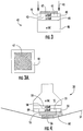
- Figure 1 is a cross-sectional schematic view of a light emitting diode broadly designated at 20 and illustrated in a manner that illustrates the potential problems than can arise when light emitting diodes mounted in certain orientations.
- the light emitting diode 20 is shown in fairly simplified fashion, it will be understood by those of ordinary skill in this art that the device 20 can be more sophisticated (i.e. include more elements) than illustrated herein. In the present circumstances, however, the invention can be clearly understood using basic illustrations.
- An exemplary diode of the type illustrated at 20 and some of its variations are also described in commonly assigned and co-pending application Publication No. US20020123164 , the contents of which are incorporated entirely herein by reference.
- the diode 20 includes a substrate 21 which maybe n-type silicon carbide having a polytype selected from the group consisting of the 2H, 4H, 6H, 8H, 15R, and 3C polytypes of silicon carbide.
- the diode portion of the device 20 is illustrated by the respective n-type gallium nitride region 22 and p-type gallium nitride region 23, which together define a p-n junction 24.
- Region 22 and region 23 may each comprise a single layer or a group of related layers having different compositions, thicknesses, dopant concentrations or other qualities.
- the diode 20 also includes an ohmic contact 25 to the p-type gallium nitride epitaxial region 23 and a die attach metal 26 in electrical contact with the ohmic contact.
- the die attach metal 26 may physically contact a bond pad (not shown) such as a gold or silver layer.
- a bond pad such as a gold or silver layer.
- reflector, barrier, and other metal layers may be formed between die attach metal 26 and the ohmic contact 25.
- Ohmic contact 15 may be formed on substrate 21 to form a vertical device as described above, and a wire lead 29 may be connected to contact 15 for connecting the device to an external circuit.
- a passivation layer 5 comprising an insulating material such as silicon nitride or silicon dioxide covers or an insulating polymer such as polyamide and protects the exposed surfaces of the epitaxial regions 22,23.
- the diode 20 is typically mounted on a metal or metallized lead frame 27, which provides an electrical contact between the diode 20 and an external circuit.
- the die attach metal 26 is formed of a metal that melts at a relatively low temperature, e.g., lower than the ohmic contact 25 and low enough such that other package components are not damaged during the die attach process. Accordingly, die attach metal 26 may comprise a solder such as tin or an alloy such as gold/tin. The die attach metal permits the diode 20 to be mounted on the lead frame quickly and easily via soldering or thermosonic bonding.
- Figure 1 also illustrates that if the die attach metal is formed imprecisely (which is always a possibility given the very small scale and size of most devices) a portion 30 of the die attach metal 26 can extend beyond the desired contact with the ohmic contact 25 and can contact the p-type gallium nitride region 23 or the n-type gallium nitride region 22. In these circumstances, the imprecise or unwanted portion 30 of the die attach metal may contact n-type gallium nitride layer 22 and can form an unwanted and parasitic Schottky diode with the n-type layer 22, or if it extends far enough, with the n-type silicon carbide substrate 21.
- Figure 2 illustrates a conventional manner of defining or isolating a junction in a light-emitting diode.
- the diode (broadly designated at 32) has been illustrated in its most fundamental aspects and can include additional elements that for the sake of clarity are not illustrated in Figure 2 .
- the diode 32 includes an n-type silicon carbide substrate 33, an n-type epitaxial layer of gallium nitride 34 on the substrate 33, and a p-type layer of gallium nitride 35 on the n-type layer, and defining the p-n junction 36.
- the epitaxial layers 34 and 35 are typically etched to form the mesa structure illustrated in the right-hand portion of Figure 2 , which also shows an ohmic contact 37 to the p-type epitaxial layer 35.
- the junction 36 within the mesa formed by etching the layers 34 and 35 is covered with silicon dioxide or some other appropriate insulating or dielectric material to help protect the junction 36 from external contamination and/or damage during die separation, packaging, or other processing steps, or during operation.
- a number of additional steps must be carried out. These typically include a masking step to define the pattern for the etch, which in turn includes the steps of laying down the mask (typically a photoresist), placing the optical pattern over the photoresist, exposing, and developing the resist, removing the developed (or as the case may be, undeveloped) portions of the mask and etching the underlying epitaxial layers, then removing the photoresist.
- a masking step to define the pattern for the etch, which in turn includes the steps of laying down the mask (typically a photoresist), placing the optical pattern over the photoresist, exposing, and developing the resist, removing the developed (or as the case may be, undeveloped) portions of the mask and etching the underlying epitaxial layers, then removing the photoresist.
- FIG 3 is a broad schematic illustration of a junction-defining method of embodiments of the present invention.
- the method comprises implanting ions represented schematically by the arrows 40 into an epitaxial layer 41 in the diode broadly designated at 42 adjacent the p-n junction 43.
- Epitaxial layer 41 has a first conductivity type (illustrated in Figure 3 as p-type).
- the type and amount of the implanted ions increase the resistivity of implanted region 44 and may render the implanted region 44 highly resistive and/or semi-insulating.
- “highly resistive” means that the material is sufficiently resistive such that negligible current flow occurs when a voltage bias is applied to the anodes of adjacent die on a wafer.
- the material in implanted regions 44 is considered highly resistive for purposes of this invention if it substantially electrically isolates adjacent die.
- the resistivity of the implanted regions 44 is at least 2000 ⁇ -cm. If the resistivity of the material is sufficiently high, the material may be considered semi-insulating (or "i-type") material rather than p-type or n-type semiconductor material. In general, material having a resistivity in excess of 1x10 5 ⁇ -cm at room temperature may be considered semi-insulating for purposes of this invention.
- the ions 40 may be implanted in a pattern that defines an implanted perimeter 44 as more clearly illustrated in Figure 3A .
- the perimeter 44 may be sufficiently doped with the implanted ions 40 to be highly resistive to thereby isolate or define the junction 43 with the implanted perimeter 44.
- Figure 3 also illustrates the n-type layer 45, the substrate 46, and the metal contact 47.
- the dashed lines in the epitaxial layer 41 also help illustrate the location of the perimeter in the view of Figure 3 .
- substrate 46 may comprise n-type silicon carbide having a polytype selected from the group consisting of the 2H, 4H, 6H, 8H, 15R, and 3C polytypes of silicon carbide. It will be appreciated by those skilled in the art, however, that substrate 46 could comprise another material such as sapphire, gallium nitride, aluminum nitride or another suitable material such as MgO, spinel, silicon or ZnO. Moreover, the substrate 46 may be conductive to permit the formation of a vertical device, or the substrate 46 could be insulating or semi-insulating.
- metal contact 47 may serve as the implant mask for implanting ions 40 into the device.
- metal contact 47 comprises a metal stack with sufficient thickness to prevent ions 40 from reaching layer 41, then it may be possible to avoid depositing a separate implant mask.
- the method comprises implanting ions such as nitrogen or phosphorus in the p-type layer of gallium nitride.
- ions such as nitrogen or phosphorus
- Other ions can be used to increase the resistivity of the region via implantation, including hydrogen, helium, aluminum and N 2 .
- Other aspects of the method will be illustrated with respect to Figure 5 .
- the implantation can be carried out in conventional fashion and at room temperature.
- the implanting ions create damage within the GaN to produce deep levels within the bandgap. These in turn trap free carriers in the GaN thus rendering the material highly resistive.
- Light-emitting diodes in Group III nitrides such as GaN are not limited to using n-type substrates and p-type top layers. There are, however, a number of reasons, well understood in this art, as to why n-type SiC substrates are more commonly used. Thus, the invention could also include implanting an n-type layer to increase its resistivity. Because the use of n-type substrates is more common, however, most of the description herein will refer to such structures.
- diode 42 can include one or more quantum wells, or superlattice structures or both and that the active layer or layers can include a greater range of the Group III nitride compounds than gallium nitride standing alone.
- active layers may also be referred to as "active layers,” “diode portions,” “diode regions,” or “diode structures,” without departing from the scope of the present invention.
- Figure 4 is a schematic cross sectional diagram similar to Figure 1 , but illustrating a diode broadly designated at 50 that incorporates the implanted perimeter region 54 of the present invention.
- the diode 50 includes a substrate, 51 which in some embodiments is n-type silicon carbide.
- n-type gallium nitrite epitaxial layer is on the substrate 51, and appears underneath the substrate 51 in the "flip-chip" orientation illustrated in Figure 4 .
- the p-type layer 53 is adjacent the n-type layer 52 and the two layers define a p-n junction 58 between them.
- the diode also includes the ohmic contact 55, and the die attach metal portion 56.
- the diode has been implanted in the manner just described with respect to Figure 3 , it includes the highly resistive perimeter portions 54 shown adjacent the dotted lines in Figure 4 .
- a portion 60 of less than ideally placed die attachment metal is also illustrated 54 on the lead frame 57.
- the invention provides several advancements. First, the geometric spatial area available for the metal portion 60 is now more limited because the implanted regions 54 of the diode 50 do not require the multiple steps necessary to form a mesa. Thus, the p-type layer and its insulated portions 54 provide an additional geometric, spatial blocking of the excess metal 60. Additionally, because the implanted portions 54 are highly resistive, there is little or no electrical interaction between the excess metal 60 and the implanted perimeter portions 54.
- the invention provides a greater margin for error when using a standard or defined amount of die attachment metal 56, 60.
- the diode 50 would have both anode and cathode connections to the lead frame but the details of these connections have been eliminated to clarify the illustration of the invention.
- the substrate 51 is illustrated in Figure 4 as being formed of conductive silicon carbide, but can also comprise semi-insulating silicon carbide or sapphire (which is insulating), because the advantages of the invention are based upon advantages provided in the epitaxial layers.
- an insulating or semi-insulating substrate requires a slightly different geometry than a conductive SiC substrate for packaging purposes, the principles with respect to the invention and the epitaxial layers remain the same.
- the substrate 51 is preferably substantially transparent to the light emitted by the junction 58 when a potential difference is applied to the device.
- the substrate is preferably substantially transparent to light having wavelengths of between about 390 and 550 nanometers, and more preferably between about 485 and 550 nanometers.
- U.S. Patent No. 5,718,760 and its siblings Nos. 6,025,289 and 6,200,917 describe techniques for producing colorless SiC. These patents are commonly assigned with the present invention, and are incorporated entirely herein by reference.
- the semiinsulating border portions 54 have sufficient resistivity to preclude Schottky behavior when the border 54 is in contact with the metal 56, 60 that would otherwise produce Schottky behavior if the border 54 were n-type.
- a light emitting diode 78 of the invention and of the type illustrated in Figure 3 or Figure 4 can be mounted in a package comprising a header 73, electrical leads 72, and an encapsulant 74 (such as epoxy) which may be molded in the shape of a lens 75.
- LED 78 may be mounted in a conventional substrate-down orientation or in a "flip-chip" orientation with the epitaxial layers adjacent the header 73.
- the resulting LED lamp 79 can be incorporated as part of a display or can be used as an indicator light, backlight or other application.
- the ohmic contacts to the p-type layer are typically selected from the group consisting of platinum, nickel, gold, titanium, aluminum, silver, and combinations of these, and when an ohmic contact is made to the silicon carbide substrate, it is usually selected from the group consisting of nickel, platinum, palladium, aluminum, titanium, and combinations thereof. Because the ohmic contacts to the substrate (not illustrated in Figure 4 ) are visibly located in the direction in which light is desirably emitted, and because larger contacts have current-spreading advantages, the ohmic contact is preferably selected and formed to be as close to transparent as possible, typically with an additional smaller bonding pad being added to enhance the flow of current to the appropriate circuit.
- the ohmic contacts 55 and the die attach metal 56 can be selected to act as a mirror or reflector to enhance the eventual output or the diode 50 when packaged and in use.
- additional metal layer or layers
- other metal layers may be included in the metal stack for other purposes, such as barrier layers for preventing diffusion of contaminants and bonding layers for bonding external contacts to the device.
- the structure of the invention is not limited to the schematic illustration of Figure 4 .
- a buffer layer is often included as part of the structure between the silicon carbide substrate and the first gallium nitride (or other Group III nitride) layer.
- the buffer layer can comprise aluminum nitride, or a graded layer of aluminum gallium nitride (AlGaN) that progresses from a higher aluminum concentration near the silicon carbide substrate to a higher gallium nitride concentration at its interface with the gallium nitride epitaxial layer.
- AlGaN aluminum gallium nitride
- Other structural portions that can be incorporated into diodes of this type and with which the invention is particularly suitable include superlattice structures for enhancing the overall crystal stability of the device, quantum wells for enhancing the output of light or tuning it to a particular frequency, or multiple quantum wells for enhancing the brightness of the device by providing the additional number of active layers and the relationships between them.
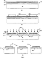
- Figure 5 illustrates some of the method aspects of the invention.
- the method electrically defines or isolates a p-n junction in a diode, most preferably in a Group III nitride or gallium nitride-based diode, to minimize or avoid undesired electrical contacts and pathways when the diode is mounted for use and/or to prevent damage to the p-n junction during die separation.
- the method comprises depositing an ohmic metal contact layer on a central portion of a p-type epitaxial layer of gallium nitride that is part of a p-n junction, patterning the metal layer by applying an etch mask on the metal layer and removing a portion of the etch mask and the metal layer, and then implanting ions into the perimeter portions of the p- type epitaxial layer that are not covered by the etch mask.
- the method can comprise masking a portion of the ohmic metal layer (and potentially a bond pad on the ohmic contact), removing the remaining exposed ohmic metal contact layer from the epitaxial layer, implanting the exposed portions of epitaxial layer with atoms sufficient to increase the resistivity of the exposed portions (and potentially render the exposed portions semi-insulating), and removing the mask from the ohmic contact (and the bond pad) to thereby produce high-resistivity portions of the p-type layer.
- the method can comprise depositing the ohmic contact and the bond pad prior to the masking step, and masking the ohmic contact metal with the photoresist.
- the diode precursor 60 includes a substrate 61 (which in certain embodiments comprises n-type SiC), an n-type gallium nitride epitaxial layer 62 on the substrate 61, a p-type gallium nitride epitaxial layer 63 on the n-type layer 62, an ohmic contact layer 65 on the p-type layer 63, and a metal bond pad 66 on the ohmic contact layer 65.
- the various steps of forming the substrate and epitaxial layers and depositing the ohmic contact and bond pad are generally well understood in the art and will not be described in detail herein.
- Figure 5(B) illustrates the diode precursor 60 after a photoresist has been deposited, masked, and patterned to form the photoresist portion 67 on all of the bond pad as illustrated in Figure 5(B) and some, but not all, areas of the ohmic contact 65.
- the precursor in Figure 5(B) is then etched to remove the portions of the ohmic contact layer 65 that are not covered by the photoresist 67.
- the etching can be carried out in any appropriate manner, with reactive ion etching (RIE) using a chlorine-based plasma being a possible method.
- RIE reactive ion etching
- the etching results in the structure shown in Figure 5(C) in which the size of the ohmic contact has been reduced to an area represented as 65(a).
- Figure 5(C) also illustrates that with a portion of the ohmic contact layer 65 removed, portions of the p-type epitaxial gallium nitride layer are uncovered.
- Figure 5(D) thus shows the implantation (schematically) of ions 70 to form the highly resistive regions 71 in the p-type gallium nitride layer 63 that define and isolate the junction 64.
- the highly resistive implanted regions 71 are semi-insulating.
- the implant step illustrated in Figure 5(D) maybe performed prior to the step of etching the ohmic contact layer 65 if the ohmic contact layer 65 is sufficiently thin so as not to substantially interfere with the implantation step.
- the precursor structure illustrated in Figure 5(E) results.
- the precursor structures may then be separated into individual die.
- the method of the invention reduces fabrication cycle time, wafer handling and chemical consumption, and likewise reduces the yield loss otherwise associated with the masking and etching procedures.
- a wafer 80 comprising a substrate 81 and epitaxial regions 82 and 83 is provided.
- a metal stack 86 is formed on epitaxial region 83.
- epitaxial region 83 has a first conductivity type and epitaxial region 82 has a second conductivity type opposite the first conductivity type.
- Each epitaxial region 82 and 83 may comprise one or more layers having the same conductivity type.
- Metal stack 86 may comprise a number of metal layers, each of which has a particular function.
- metal stack 86 may comprise a layer of metal for forming an ohmic contact with epitaxial region 83.
- Metal stack 86 may also comprise reflector, barrier, adhesion, bonding, and/or other layers.
- etch mask 85 is deposited on metal stack 86 and patterned via photolithography to form openings that selectively reveal surface portions 86A of metal stack 86.
- metal stack 86 could be formed by photolithography, deposition and liftoff techniques which are well known in the art. That is, metal stack 86 could be formed by applying a blanket photoresist to the surface of the epitaxial region 83, patterning the photoresist by exposing and developing it, depositing the metal as a blanket layer and lifting off the unwanted metal.
- metal stack 86 is selectively etched to reveal surface portions 83A of epitaxial region 83.
- Etch mask 85 is then removed by conventional methods.
- Ions 87 are then implanted into the exposed portions of epitaxial region 83 to render the implanted regions 84 highly resistive in the manner described above and to define p-n junction regions 88 within the structure.
- the patterned metal layer 86 serves as the implant mask.
- the etch/implant mask 85 is removed and individual die 89 are separated using conventional techniques such that defined p-n junction regions 88 are spaced apart from the sidewalls 90 of the die, and are thereby physically and electrically isolated.
- N +1 nitrogen was implanted at 20 keV at a dosage of 10 13 cm -2 followed by a dosage at 125 keV of monovalent nitrogen at 1.4 x 10 13 cm -2 .
- the first dosage was carried out at 20 keV using N +1 at a dosage of 10 13 cm -2 , followed by 125 keV of at a dosage of 1.4 x 10 13 cm -2 followed by 190 keV of N +1 at 1.7 x 10 13 cm -2 .
- junction isolation was verified by probing adjacent metal stacks and performing a continuity measurement. No measurable current was observed prior to breakdown of the p-n junction. Implanted helium and hydrogen have also created resistivity conditions leading to the potential conclusion that implanting almost any ion into p-type gallium nitride at room temperature will cause the material to become dramatically more resistant.
- junction isolation by this technique appears to lend itself to any nitride device that incorporates a p-type layer. For this reason, nitride based light emitting diodes on sapphire as well as on silicon carbide and other substrates appear to benefit equally from the use of implantation for junction isolation.
- the standard implant condition was (1) below. Other conditions (2) - (5). were also examined.
- the (2) condition was intended to evaluate the number of carriers that are eliminated per implanted ion.
- Conditions (3) and (5) were intended to evaluate the effect of implanting on the p-side of the device only.
- Condition (4) evaluated the efficiency of trapping carriers similar to the (1) and (2) comparison. In carrying out the implantations, it was determined that higher energy implants were needed for Cree's green LEDs as compared to Cree's blue LEDs.
- the 190 keV implant of (1) and (2) goes far deeper than the p-n junction placing most of the 190 keV implanted nitrogen on the n-side.
- the single dose at 125 keV of (3) and (4) and the double dose of (5) were considered.
- the 100 and 125 keV energies place the peak of the nitrogen concentration at or about the p-n junction which is 1500 - 1800 A below the surface.
- the simulated peak for the 100 and 125 keV implants is about 1600 and 2000 A, respectively.
- the GaN material is converted from low resistivity to high resistivity.
- P-type GaN is about 1200 - 1500 A thick with a free hole concentration of about 2 - 5 E17/cm 3
- P-type AlGaN is about 300 A thick with a hole concentration of about 5 - 20 E 16/cm 3
- each of conditions (1)-(5) created high resistivity p-type material and isolated adjacent devices, but none produced good ESD yield.
- the addition of a further 230 keV nitrogen implant with a dose of 2 E 13/cm 2 worked well for isolation and ESD yield.
- the resistivity was estimated to be greater than 2 x 10 3 ohm-cm. This was done by evaluating the current flowing between two adjacent pads with an applied voltage of 2 Volts. The resulting current was unmeasurable ( ⁇ 50 nA). This corresponds to a resistance greater than 40 x 10 6 ohms. The distance between the pads is 70 microns and the width is 230 microns. The number of squares is then about 0.3 between them. The effects of fringing were ignored to give the estimate a worst case lower limit on resistivity. This gives a lower limit on the sheet resistance of 133 x 10 6 ohms per square. Taking the thickness to be 0.15 x 10 -4 cm thick yields a resistivity of greater than 2000 ohm-cm.
Landscapes
- Engineering & Computer Science (AREA)
- Manufacturing & Machinery (AREA)
- Computer Hardware Design (AREA)
- Microelectronics & Electronic Packaging (AREA)
- Power Engineering (AREA)
- Led Devices (AREA)
- Led Device Packages (AREA)
- Recrystallisation Techniques (AREA)
Claims (25)
- Licht-emittierende Diode (42, 50), die auf einem Lead-Frame (57) angebracht ist, wobei sie aufweist:• ein Halbleitersubstrat (46, 51);• einen ersten epitaxialen Bereich (45, 52) von Gruppe III-Nitrid auf dem Substrat, wobei der epitaxiale Bereich einen ersten Leitfähigkeitstyp aufweist;• einen zweiten epitaxialen Bereich (41, 53) von Gruppe III-Nitrid auf dem ersten epitaxialen Bereich, wobei der zweite epitaxiale Bereich einen vom erste epitaxialen Bereich entgegengesetzten Leitfähigkeitstyp aufweist;• wobei die ersten und zweiten epitaxialen Bereiche zwischen sich einen p-n-Übergang (43, 58) bilden;• einen Metallkontakt (47, 55) auf dem zweiten epitaxialen Bereich entgegengesetzt von dem ersten epitaxialen Bereich; und• einen Gruppe III-Nitrid-Isolierbereich (44, 54), der den zweiten epitaxialen Bereich umgibt, mit einem erhöhten spezifischen Widerstand im Vergleich zum zweiten epitaxialen Bereich, zum elektrischen Isolieren von Abschnitten des p-n-Übergangs,gekennzeichnet durch:• ein Die-Attach-Material (56, 60), das bei einer tieferen Temperatur als der Metallkontakt (47, 45) zwischen dem Metallkontakt und dem Lead-Frame (57) schmilzt;• wobei der erste epitaxiale Bereich einen Abschnitt enthält, der sich über einen Außenumfang des Metallkontakts hinaus auswärts erstreckt;• wobei der Metallkontakt (47, 55) an dem Lead-Frame durch das Die-Attach-Material angebracht ist, wobei der Isolierbereich Abschnitte des p-n-Übergangs von dem Lead-Frame und dem Die-Attach-Material elektrisch isoliert; und• wobei der Gruppe III-Isolierbereich auf dem Abschnitt des epitaxialen Bereichs ist, der sich über den Außenumfang des Metallkontakts hinaus auswärts erstreckt.
- Licht-emittierende Diode nach Anspruch 1, wobei der Isolierbereich (44, 54) einen größeren spezifischen Widerstand als etwa 2000 Ω-cm hat.
- Licht-emittierende Diode nach Anspruch 1, wobei der Isolierbereich (44, 54) semi-isolierend ist.
- Licht-emittierende Diode nach Anspruch 3, wobei der Metallkontakt (47, 55) aus der Gruppe ausgewählt ist, bestehend aus Ohm'schen Kontakten, reflektiven Schichten und Bondingschichten.
- Licht-emittierende Diode nach Anspruch 1, wobei das Substrat (46, 51) ein Material aufweist, das aus der Gruppe ausgewählt ist, bestehend aus Silizium-Carbid, Saphir, ZnO, MgO, Spinell, Silizium, Gallium-Nitrid und Aluminium-Nitrid.
- Licht-emittierende Diode nach Anspruch 1, wobei das Substrat (46, 51) aus der Gruppe ausgewählt ist, bestehend aus leitfähigen Substraten und semi-isolierenden Substraten.
- Licht-emittierende Diode nach Anspruch 1, die ferner eine Passivierungsschicht auf den epitaxialen Bereichen aufweist und aus der Gruppe gewählt ist, bestehend aus Silizium-Nitrid, Silizium-Dioxid und isolierenden Polymeren.
- Licht-emittierende Halbleiterdiode nach Anspruch 1, welche aufweist:eine Pufferschicht auf dem Substrat zwischen dem Substrat (46, 51) und dem ersten epitaxialen Bereich (45, 52);wobei die ersten und zweiten epitaxialen Bereiche zumindest einen Abschnitt einer aktiven Halbleiterstruktur auf der Pufferschicht bilden, um für eine optische Emission zu sorgen, wenn Strom dort hindurchgeschickt wird;einen epitaxialen p-Typ-Bereich (41, 53) von einem Gruppe III-Nitrid auf der aktiven Struktur;wobei der Isolierbereich (44, 54) eine Gallium-Nitrid-Grenze mit hohem spezifischem Widerstand auf der aktiven Struktur aufweist und die p-Typ-Schicht umgibt, um Abschnitte der aktiven Struktur elektrisch zu isolieren; undeinen zweiten Metallkontakt zu der Diode zum Schicken von Strom durch die Diode und die aktive Struktur und Erzeugen einer gewünschten Emission von dieser.
- Licht-emittierende Diode nach Anspruch 8, wobei die Grenze mit hohem spezifischem Widerstand einen ausreichenden spezifischen Widerstand hat, um ein Schottky-Verhalten auszuschließen, wenn die Grenze mit Metall in Kontakt ist.
- Licht-emittierende Diode nach Anspruch 1, wobei:das Substrat (46, 51) ein leitfähiges Silizium-Carbid-Substrat vom n-Typ ist;der erste Gruppe III-Nitrid-Bereich (45, 52) vom n-Typ ist; undder zweite Gruppe III-Nitrid-Bereich (41, 53) vom p-Typ ist.
- Verfahren zum Herstellen einer Licht-emittierenden Diode (42, 50), welches aufweist:Bilden eines ersten epitaxialen Bereichs (45, 52) mit einem ersten Leitfähigkeitstyp auf einem Substrat;Bilden eines zweiten epitaxialen Bereichs (41, 53) mit einem zweiten Leifähigkeitstyp auf dem ersten epitaxialen Bereich, wobei die ersten und zweiten epitaxialen Bereiche einen p-n-Übergang (43, 58) bilden;Auftragen eines Metallkontakts (47, 55) auf einen mittleren Abschnitt einer Oberfläche des zweiten epitaxialen Bereichs entgegengesetzt vom ersten epitaxialen Bereich, wobei der Metallkontakt Umfangsabschnitte (44, 54) der Oberfläche des zweiten epitaxialen Bereichs freilegt;Implantieren von Ionen (40, 70) in die Umfangsabschnitte (44, 54) des zweiten epitaxialen Bereichs durch die freiliegenden Umfangsabschnitte, um einen implantierten Umfang zu definieren, der mit den implantierten Ionen ausreichend dotiert ist, so dass er einen hohen spezifischen Widerstand hat, um hierdurch den p-n-Übergang (41, 58) innerhalb des implantierten Umfangs zu isolieren; undPositionieren der Licht-emittierenden Diode auf einem Lead-Frame (57) unter Verwendung von Die-Attach-Material, das zwischen dem Metallkontakt und dem Lead-Frame angeordnet ist, so dass der Umfangsabschnitt des zweiten epitaxialen Bereichs mit hohem spezifischem Widerstand, der durch den Metallkontakt freiliegt, den p-n-Übergang von dem Lead-Frame und dem Die-Attach-Material isoliert.
- Das Verfahren nach Anspruch 11, das ferner aufweist:Aufbringen eines Photoresists (67) auf den Metallkontakt,Bemustern des Photoresists; undselektives Ätzen von Abschnitten des Metallkontakts, um Abschnitte der Oberfläche des zweiten epitaxialen Bereichs (41, 53) freizulegen.
- Das Verfahren nach Anspruch 12, das ferner aufweist, das Photoresist (67) vor dem Implantieren von Ionen in den zweiten epitaxialen Bereich (41, 53) zu entfernen.
- Das Verfahren nach Anspruch 13, das ferner aufweist, Ionen in den zweiten epitaxialen Bereich (41, 53) vor dem Entfernen des Photoresists zu implantieren.
- Das Verfahren von Anspruch 12, das ferner aufweist, eine Passivierungsschicht auf freiliegende Abschnitte des zweiten epitaxialen Bereichs (41, 53) aufzutragen, welche aus der Gruppe ausgewählt ist, bestehend aus Silizium-Dioxid, Silizium-Nitrid, isolierenden Polymeren und Kombinationen davon.
- Das Verfahren nach Anspruch 11, das ferner aufweist, Ionen zu implantieren, die aus der Gruppe ausgewählt sind, bestehend aus Stickstoff, Phosphor, Aluminium, Helium, Wasserstoff und N2.
- Verfahren nach Anspruch 11, das aufweist, Ionen zu dem epitaxialen p-Typ-Bereich (41, 53) von Gallium-Nitrid zu lenken.
- Verfahren nach Anspruch 11, das aufweist, eine Maske auf der Oberfläche des ersten epitaxialen Bereichs (45, 52) vor dem Schritt des Implantierens von Ionen aufzutragen.
- Verfahren nach Anspruch 18, wobei der Schritt des Auftragens der Maske aufweist, eine gemusterte Metallschicht aufzutragen, die einen Metallkontakt (47, 55) an dem ersten epitaxialen Bereich vorsehen kann.
- Verfahren nach Anspruch 11, wobei der Schritt des Lenkens der Implantier-Ionen zumindest zwei Implantierschritte aufweist, die sich voneinander gemäß einem Faktor unterscheiden, der aus der Gruppe ausgewählt ist, bestehend aus Ionenenergie, Ionendosis und Kombinationen davon.
- Verfahren nach Anspruch 11, das aufweist, Ionen mit einer Dosis von zwischen etwa 1 bis 2 x 1013 cm-2 mit Energien von zwischen etwa 100 und 200 keV in einen epitaxialen Bereich (41, 53) zu implantieren, der eine p-Typ-Trägerkonzentration von etwa 1 x 1017 cm-3 aufweist.
- Verfahren nach Anspruch 11, das aufweist, eine Vorrichtung oder deren Vorläufer passivieren, die oder der zumindest einen epitaxialen p-Typ-Bereich (41, 53), einen Metallkontakt (47, 55) auf der p-Typ-Schicht sowie ein Bond-Pad auf dem Metallkontakt enthält, durch:Maskieren eines Abschnitts des Metallkontakts (47, 55) und des gesamten Bond-Pads;Entfernen des verbleibenden freiliegenden Metallkontakts (47, 55) von dem epitaxialen Bereich (41, 53);Implantieren der freigelegten Abschnitte (44, 54) des epitaxialen Bereichs (41, 53) mit Ionen, ausreichend, um den freigelegten Abschnitten einen hohen spezifischen Widerstand zu verleihen; undEntfernen der Maske von dem Metallkontakt und dem Bond-Pad, um hierdurch passivierte Abschnitte der p-Typ-Schicht herzustellen.
- Verfahren von Anspruch 11, das aufweist, den Metallkontakt (47, 55) und das Bond-Pad vor dem Maskierungsschritt aufzutragen.
- Verfahren nach Anspruch 11, das aufweist, den Metallkontakt (47, 55) mit einem Photoresist zu maskieren.
- Die Licht-emittierende Diode von Anspruch 1, wobei eine Innengrenze des Isolierbereichs (44, 54) einem Außenumfang des Metallkontakts (47, 55) entspricht.
Applications Claiming Priority (2)
| Application Number | Priority Date | Filing Date | Title |
|---|---|---|---|
| US32018203P | 2003-05-09 | 2003-05-09 | |
| PCT/US2004/014023 WO2004102686A1 (en) | 2003-05-09 | 2004-05-06 | Led fabrication via ion implant isolation |
Publications (2)
| Publication Number | Publication Date |
|---|---|
| EP1623467A1 EP1623467A1 (de) | 2006-02-08 |
| EP1623467B1 true EP1623467B1 (de) | 2016-12-07 |
Family
ID=33449503
Family Applications (1)
| Application Number | Title | Priority Date | Filing Date |
|---|---|---|---|
| EP04751419.5A Expired - Lifetime EP1623467B1 (de) | 2003-05-09 | 2004-05-06 | LED-Herstellung durch Ionenimplantationsisolierung |
Country Status (6)
| Country | Link |
|---|---|
| US (1) | US7338822B2 (de) |
| EP (1) | EP1623467B1 (de) |
| JP (2) | JP5122817B2 (de) |
| CN (2) | CN101697366B (de) |
| TW (1) | TWI347683B (de) |
| WO (1) | WO2004102686A1 (de) |
Families Citing this family (46)
| Publication number | Priority date | Publication date | Assignee | Title |
|---|---|---|---|---|
| JP5122817B2 (ja) * | 2003-05-09 | 2013-01-16 | クリー インコーポレイテッド | イオン・インプラント・アイソレーションによるled製作 |
| JP4766845B2 (ja) * | 2003-07-25 | 2011-09-07 | シャープ株式会社 | 窒化物系化合物半導体発光素子およびその製造方法 |
| TWI241030B (en) * | 2003-09-19 | 2005-10-01 | Tinggi Technologies Pte Ltd | Fabrication of conductive metal layer on semiconductor devices |
| US8034643B2 (en) | 2003-09-19 | 2011-10-11 | Tinggi Technologies Private Limited | Method for fabrication of a semiconductor device |
| US20050194584A1 (en) * | 2003-11-12 | 2005-09-08 | Slater David B.Jr. | LED fabrication via ion implant isolation |
| ATE533187T1 (de) * | 2004-03-15 | 2011-11-15 | Tinggi Technologies Private Ltd | Fabrikation von halbleiterbauelementen |
| WO2005098974A1 (en) * | 2004-04-07 | 2005-10-20 | Tinggi Technologies Private Limited | Fabrication of reflective layer on semiconductor light emitting diodes |
| US7592634B2 (en) * | 2004-05-06 | 2009-09-22 | Cree, Inc. | LED fabrication via ion implant isolation |
| US8174037B2 (en) | 2004-09-22 | 2012-05-08 | Cree, Inc. | High efficiency group III nitride LED with lenticular surface |
| SG130975A1 (en) | 2005-09-29 | 2007-04-26 | Tinggi Tech Private Ltd | Fabrication of semiconductor devices for light emission |
| SG131803A1 (en) | 2005-10-19 | 2007-05-28 | Tinggi Tech Private Ltd | Fabrication of transistors |
| SG133432A1 (en) | 2005-12-20 | 2007-07-30 | Tinggi Tech Private Ltd | Localized annealing during semiconductor device fabrication |
| KR20080106402A (ko) | 2006-01-05 | 2008-12-05 | 일루미텍스, 인크. | Led로부터 광을 유도하기 위한 개별 광학 디바이스 |
| JP2008041811A (ja) * | 2006-08-03 | 2008-02-21 | Ngk Spark Plug Co Ltd | 配線基板および多数個取り配線基板ならびにその製造方法 |
| SG140473A1 (en) | 2006-08-16 | 2008-03-28 | Tinggi Tech Private Ltd | Improvements in external light efficiency of light emitting diodes |
| US7646024B2 (en) * | 2006-08-18 | 2010-01-12 | Cree, Inc. | Structure and method for reducing forward voltage across a silicon carbide-group III nitride interface |
| SG140512A1 (en) * | 2006-09-04 | 2008-03-28 | Tinggi Tech Private Ltd | Electrical current distribution in light emitting devices |
| CN101553928B (zh) | 2006-10-02 | 2011-06-01 | 伊鲁米特克有限公司 | Led系统和方法 |
| US8674593B2 (en) * | 2007-05-31 | 2014-03-18 | Nthdegree Technologies Worldwide Inc | Diode for a printable composition |
| EP2240968A1 (de) | 2008-02-08 | 2010-10-20 | Illumitex, Inc. | System und verfahren zur bildung einer emitterschicht |
| US20090261346A1 (en) * | 2008-04-16 | 2009-10-22 | Ding-Yuan Chen | Integrating CMOS and Optical Devices on a Same Chip |
| TW201034256A (en) | 2008-12-11 | 2010-09-16 | Illumitex Inc | Systems and methods for packaging light-emitting diode devices |
| JP2010199558A (ja) * | 2009-01-27 | 2010-09-09 | Panasonic Corp | 半導体装置およびその製造方法 |
| US8096671B1 (en) | 2009-04-06 | 2012-01-17 | Nmera, Llc | Light emitting diode illumination system |
| US8585253B2 (en) | 2009-08-20 | 2013-11-19 | Illumitex, Inc. | System and method for color mixing lens array |
| US8449128B2 (en) | 2009-08-20 | 2013-05-28 | Illumitex, Inc. | System and method for a lens and phosphor layer |
| US8263422B2 (en) * | 2010-04-26 | 2012-09-11 | Varian Semiconductor Equipment Associates, Inc. | Bond pad isolation and current confinement in an LED using ion implantation |
| DE102010026518A1 (de) | 2010-07-08 | 2012-01-12 | Osram Opto Semiconductors Gmbh | Leuchtdiodenchip und Verfahren zur Herstellung eines Leuchtdiodenchips |
| KR101782081B1 (ko) * | 2010-08-30 | 2017-09-26 | 엘지이노텍 주식회사 | 발광 소자 |
| US20120097918A1 (en) * | 2010-10-20 | 2012-04-26 | Varian Semiconductor Equipment Associates, Inc. | Implanted current confinement structure to improve current spreading |
| US8664027B2 (en) | 2011-02-11 | 2014-03-04 | Varian Semiconductor Associates, Inc. | LED mesa sidewall isolation by ion implantation |
| US8927999B2 (en) * | 2011-11-21 | 2015-01-06 | Avogy, Inc. | Edge termination by ion implantation in GaN |
| DE102012108883A1 (de) * | 2012-09-20 | 2014-03-20 | Osram Opto Semiconductors Gmbh | Optoelektronischer Halbleiterchip und Verfahren zur Herstellung von optoelektronischen Halbleiterchips |
| TWI495154B (zh) * | 2012-12-06 | 2015-08-01 | Genesis Photonics Inc | 半導體結構 |
| US9985190B2 (en) * | 2016-05-18 | 2018-05-29 | eLux Inc. | Formation and structure of post enhanced diodes for orientation control |
| CN106711301B (zh) * | 2015-11-12 | 2020-10-27 | 美科米尚技术有限公司 | 发光二极管与其制作方法 |
| CN106024623B (zh) * | 2016-06-29 | 2019-03-01 | 江苏能华微电子科技发展有限公司 | 一种氮化镓肖特基二极管及其制作方法 |
| TWI703726B (zh) | 2016-09-19 | 2020-09-01 | 新世紀光電股份有限公司 | 含氮半導體元件 |
| US10892137B2 (en) * | 2018-09-12 | 2021-01-12 | Entegris, Inc. | Ion implantation processes and apparatus using gallium |
| DE102019129619A1 (de) * | 2019-11-04 | 2021-05-06 | OSRAM Opto Semiconductors Gesellschaft mit beschränkter Haftung | Optoelektronisches halbleiterbauteil |
| GB2590450B (en) * | 2019-12-18 | 2022-01-05 | Plessey Semiconductors Ltd | Light emitting diode precursor |
| CN111653565B (zh) * | 2020-03-11 | 2023-03-17 | 厦门市三安集成电路有限公司 | 一种高阻抗半导体电阻器结构及其制备方法 |
| US11227801B2 (en) | 2020-03-19 | 2022-01-18 | International Business Machines Corporation | Formation of contacts for semiconductor devices |
| CN114864760A (zh) * | 2021-02-03 | 2022-08-05 | 厦门三安光电有限公司 | 微型发光二极管和显示面板 |
| CN114141916B (zh) * | 2021-11-24 | 2023-08-01 | 福州大学 | 纳米尺寸led芯片阵列及其制备方法 |
| CN114628432B (zh) * | 2022-02-28 | 2023-03-10 | 诺视科技(苏州)有限公司 | 一种半导体装置的制作方法及半导体装置 |
Citations (1)
| Publication number | Priority date | Publication date | Assignee | Title |
|---|---|---|---|---|
| US3824133A (en) * | 1971-12-02 | 1974-07-16 | Bell Telephone Labor Inc | Fabrication of electrically insulating regions in optical devices by proton bombardment |
Family Cites Families (43)
| Publication number | Priority date | Publication date | Assignee | Title |
|---|---|---|---|---|
| US5114827A (en) * | 1988-06-28 | 1992-05-19 | Microelectronics Center Of N.C. | Photoresists resistant to oxygen plasmas |
| US4968582A (en) * | 1988-06-28 | 1990-11-06 | Mcnc And University Of Nc At Charlotte | Photoresists resistant to oxygen plasmas |
| US5119540A (en) * | 1990-07-24 | 1992-06-09 | Cree Research, Inc. | Apparatus for eliminating residual nitrogen contamination in epitaxial layers of silicon carbide and resulting product |
| JPH0394481A (ja) | 1989-09-07 | 1991-04-19 | Ricoh Co Ltd | アレイ状半導体発光装置 |
| US5210051A (en) * | 1990-03-27 | 1993-05-11 | Cree Research, Inc. | High efficiency light emitting diodes from bipolar gallium nitride |
| US5248760A (en) * | 1991-01-25 | 1993-09-28 | Unc At Charlotte | Chemically cured low temperature polyimides |
| JPH0546052U (ja) * | 1991-11-19 | 1993-06-18 | 三洋電機株式会社 | 発光ダイオード装置 |
| JPH0697498A (ja) * | 1992-09-17 | 1994-04-08 | Toshiba Corp | 半導体発光素子 |
| US5393642A (en) * | 1992-12-31 | 1995-02-28 | The University Of North Carolina At Charlotte | Ionic modification of organic resins and photoresists to produce photoactive etch resistant compositions |
| US5416342A (en) * | 1993-06-23 | 1995-05-16 | Cree Research, Inc. | Blue light-emitting diode with high external quantum efficiency |
| US5393993A (en) * | 1993-12-13 | 1995-02-28 | Cree Research, Inc. | Buffer structure between silicon carbide and gallium nitride and resulting semiconductor devices |
| US5449925A (en) * | 1994-05-04 | 1995-09-12 | North Carolina State University | Voltage breakdown resistant monocrystalline silicon carbide semiconductor devices |
| US5592501A (en) * | 1994-09-20 | 1997-01-07 | Cree Research, Inc. | Low-strain laser structures with group III nitride active layers |
| US5631190A (en) * | 1994-10-07 | 1997-05-20 | Cree Research, Inc. | Method for producing high efficiency light-emitting diodes and resulting diode structures |
| US5679153A (en) * | 1994-11-30 | 1997-10-21 | Cree Research, Inc. | Method for reducing micropipe formation in the epitaxial growth of silicon carbide and resulting silicon carbide structures |
| SE9500146D0 (sv) | 1995-01-18 | 1995-01-18 | Abb Research Ltd | Halvledarkomponent i kiselkarbid |
| US5718760A (en) * | 1996-02-05 | 1998-02-17 | Cree Research, Inc. | Growth of colorless silicon carbide crystals |
| JP3688843B2 (ja) * | 1996-09-06 | 2005-08-31 | 株式会社東芝 | 窒化物系半導体素子の製造方法 |
| US5866925A (en) * | 1997-01-09 | 1999-02-02 | Sandia Corporation | Gallium nitride junction field-effect transistor |
| US6217662B1 (en) * | 1997-03-24 | 2001-04-17 | Cree, Inc. | Susceptor designs for silicon carbide thin films |
| JPH10294491A (ja) | 1997-04-22 | 1998-11-04 | Toshiba Corp | 半導体発光素子およびその製造方法ならびに発光装置 |
| US6201262B1 (en) * | 1997-10-07 | 2001-03-13 | Cree, Inc. | Group III nitride photonic devices on silicon carbide substrates with conductive buffer interlay structure |
| US6063186A (en) * | 1997-12-17 | 2000-05-16 | Cree, Inc. | Growth of very uniform silicon carbide epitaxial layers |
| JP3516433B2 (ja) * | 1997-12-19 | 2004-04-05 | 昭和電工株式会社 | 化合物半導体発光素子 |
| US5998232A (en) * | 1998-01-16 | 1999-12-07 | Implant Sciences Corporation | Planar technology for producing light-emitting devices |
| JPH11214800A (ja) * | 1998-01-28 | 1999-08-06 | Sony Corp | 半導体装置およびその製造方法 |
| US6090300A (en) * | 1998-05-26 | 2000-07-18 | Xerox Corporation | Ion-implantation assisted wet chemical etching of III-V nitrides and alloys |
| JP2000077713A (ja) * | 1998-08-27 | 2000-03-14 | Sanyo Electric Co Ltd | 半導体発光素子 |
| US6459100B1 (en) * | 1998-09-16 | 2002-10-01 | Cree, Inc. | Vertical geometry ingan LED |
| US6331450B1 (en) * | 1998-12-22 | 2001-12-18 | Toyoda Gosei Co., Ltd. | Method of manufacturing semiconductor device using group III nitride compound |
| US6432788B1 (en) * | 1999-07-22 | 2002-08-13 | Implant Sciences Corporation | Method for fabricating an emitter-base junction for a gallium nitride bipolar transistor |
| US6812053B1 (en) * | 1999-10-14 | 2004-11-02 | Cree, Inc. | Single step pendeo- and lateral epitaxial overgrowth of Group III-nitride epitaxial layers with Group III-nitride buffer layer and resulting structures |
| JP3424634B2 (ja) * | 2000-01-27 | 2003-07-07 | 日亜化学工業株式会社 | 窒化物半導体レーザ素子 |
| JP2001237499A (ja) * | 2000-02-22 | 2001-08-31 | Sony Corp | 半導体発光素子の製造方法 |
| TW493284B (en) * | 2000-09-06 | 2002-07-01 | Highlink Technology Corp | LED device and the manufacturing method thereof |
| US6255129B1 (en) * | 2000-09-07 | 2001-07-03 | Highlink Technology Corporation | Light-emitting diode device and method of manufacturing the same |
| US20020096496A1 (en) * | 2000-11-29 | 2002-07-25 | Bela Molnar | Patterning of GaN crystal films with ion beams and subsequent wet etching |
| US6800876B2 (en) * | 2001-01-16 | 2004-10-05 | Cree, Inc. | Group III nitride LED with undoped cladding layer (5000.137) |
| US6791119B2 (en) * | 2001-02-01 | 2004-09-14 | Cree, Inc. | Light emitting diodes including modifications for light extraction |
| US6547249B2 (en) * | 2001-03-29 | 2003-04-15 | Lumileds Lighting U.S., Llc | Monolithic series/parallel led arrays formed on highly resistive substrates |
| JP3765246B2 (ja) | 2001-06-06 | 2006-04-12 | 豊田合成株式会社 | Iii族窒化物系化合物半導体発光素子の製造方法 |
| US6740906B2 (en) * | 2001-07-23 | 2004-05-25 | Cree, Inc. | Light emitting diodes including modifications for submount bonding |
| JP5122817B2 (ja) * | 2003-05-09 | 2013-01-16 | クリー インコーポレイテッド | イオン・インプラント・アイソレーションによるled製作 |
-
2004
- 2004-05-06 JP JP2006532792A patent/JP5122817B2/ja not_active Expired - Lifetime
- 2004-05-06 CN CN2009102088552A patent/CN101697366B/zh not_active Expired - Lifetime
- 2004-05-06 US US10/840,463 patent/US7338822B2/en not_active Expired - Lifetime
- 2004-05-06 CN CN2004800125618A patent/CN1802755B/zh not_active Expired - Lifetime
- 2004-05-06 WO PCT/US2004/014023 patent/WO2004102686A1/en active Search and Examination
- 2004-05-06 EP EP04751419.5A patent/EP1623467B1/de not_active Expired - Lifetime
- 2004-05-07 TW TW093112923A patent/TWI347683B/zh not_active IP Right Cessation
-
2011
- 2011-03-15 JP JP2011056687A patent/JP5491439B2/ja not_active Expired - Lifetime
Patent Citations (1)
| Publication number | Priority date | Publication date | Assignee | Title |
|---|---|---|---|---|
| US3824133A (en) * | 1971-12-02 | 1974-07-16 | Bell Telephone Labor Inc | Fabrication of electrically insulating regions in optical devices by proton bombardment |
Also Published As
| Publication number | Publication date |
|---|---|
| US20060108595A9 (en) | 2006-05-25 |
| JP2011187966A (ja) | 2011-09-22 |
| WO2004102686A1 (en) | 2004-11-25 |
| CN1802755B (zh) | 2012-05-16 |
| US20050029533A1 (en) | 2005-02-10 |
| JP5122817B2 (ja) | 2013-01-16 |
| JP5491439B2 (ja) | 2014-05-14 |
| CN1802755A (zh) | 2006-07-12 |
| TWI347683B (en) | 2011-08-21 |
| TW200501459A (en) | 2005-01-01 |
| EP1623467A1 (de) | 2006-02-08 |
| US7338822B2 (en) | 2008-03-04 |
| CN101697366A (zh) | 2010-04-21 |
| JP2006528435A (ja) | 2006-12-14 |
| CN101697366B (zh) | 2012-12-19 |
Similar Documents
| Publication | Publication Date | Title |
|---|---|---|
| EP1623467B1 (de) | LED-Herstellung durch Ionenimplantationsisolierung | |
| US7943406B2 (en) | LED fabrication via ion implant isolation | |
| US7592634B2 (en) | LED fabrication via ion implant isolation | |
| US6998642B2 (en) | Series connection of two light emitting diodes through semiconductor manufacture process | |
| US6838704B2 (en) | Light emitting diode and method of making the same | |
| JP4699258B2 (ja) | フリップチップ発光ダイオード及びその製造方法 | |
| US6853011B2 (en) | Light emitting diode and method of making the same | |
| KR100609118B1 (ko) | 플립 칩 발광다이오드 및 그 제조방법 | |
| US20060202225A1 (en) | Submount for use in flipchip-structured light emitting device including transistor | |
| WO2012091311A2 (en) | High efficiency light emitting diode | |
| KR100431760B1 (ko) | AlGaInN계 반도체 엘이디(LED) 소자 및 그 제조 방법 | |
| KR100691497B1 (ko) | 발광 소자 및 이의 제조 방법 | |
| KR101719623B1 (ko) | 발광소자 | |
| KR101171356B1 (ko) | 다수의 셀이 결합된 발광 소자 및 이의 제조 방법 | |
| CN110021691B (zh) | 一种半导体发光器件 | |
| KR101203138B1 (ko) | 발광소자와 그 제조방법 | |
| KR101916369B1 (ko) | 발광 다이오드 | |
| KR100646635B1 (ko) | 복수 셀의 단일 발광 소자 및 이의 제조 방법 | |
| KR101773582B1 (ko) | 고효율 발광 다이오드 | |
| KR100663910B1 (ko) | 발광 소자 및 이의 제조 방법 | |
| KR100663907B1 (ko) | 다수의 셀이 결합된 발광 소자 및 이의 제조 방법 | |
| KR100644215B1 (ko) | 발광소자와 그 제조방법 | |
| KR101633814B1 (ko) | 발광 소자 |
Legal Events
| Date | Code | Title | Description |
|---|---|---|---|
| PUAI | Public reference made under article 153(3) epc to a published international application that has entered the european phase |
Free format text: ORIGINAL CODE: 0009012 |
|
| 17P | Request for examination filed |
Effective date: 20051108 |
|
| AK | Designated contracting states |
Kind code of ref document: A1 Designated state(s): AT BE BG CH CY CZ DE DK EE ES FI FR GB GR HU IE IT LI LU MC NL PL PT RO SE SI SK TR |
|
| DAX | Request for extension of the european patent (deleted) | ||
| RIN1 | Information on inventor provided before grant (corrected) |
Inventor name: SUVOROV, ALEXANDER Inventor name: TSVETKOV, VALERI, F. Inventor name: NEGLEY, GERALD, H. Inventor name: SLATER, JR., DAVID, B. Inventor name: WU, YIFENG |
|
| 17Q | First examination report despatched |
Effective date: 20070613 |
|
| REG | Reference to a national code |
Ref country code: DE Ref legal event code: R079 Ref document number: 602004050447 Country of ref document: DE Free format text: PREVIOUS MAIN CLASS: H01L0033000000 Ipc: H01L0033140000 |
|
| GRAP | Despatch of communication of intention to grant a patent |
Free format text: ORIGINAL CODE: EPIDOSNIGR1 |
|
| RIC1 | Information provided on ipc code assigned before grant |
Ipc: H01L 33/32 20100101ALN20160711BHEP Ipc: H01L 33/14 20100101AFI20160711BHEP Ipc: H01L 33/02 20100101ALI20160711BHEP Ipc: H01L 33/00 20100101ALI20160711BHEP |
|
| INTG | Intention to grant announced |
Effective date: 20160727 |
|
| RIC1 | Information provided on ipc code assigned before grant |
Ipc: H01L 33/32 20100101ALN20160715BHEP Ipc: H01L 33/00 20100101ALI20160715BHEP Ipc: H01L 33/02 20100101ALI20160715BHEP Ipc: H01L 33/14 20100101AFI20160715BHEP |
|
| GRAS | Grant fee paid |
Free format text: ORIGINAL CODE: EPIDOSNIGR3 |
|
| GRAA | (expected) grant |
Free format text: ORIGINAL CODE: 0009210 |
|
| AK | Designated contracting states |
Kind code of ref document: B1 Designated state(s): AT BE BG CH CY CZ DE DK EE ES FI FR GB GR HU IE IT LI LU MC NL PL PT RO SE SI SK TR |
|
| REG | Reference to a national code |
Ref country code: GB Ref legal event code: FG4D |
|
| REG | Reference to a national code |
Ref country code: CH Ref legal event code: EP Ref country code: AT Ref legal event code: REF Ref document number: 852411 Country of ref document: AT Kind code of ref document: T Effective date: 20161215 |
|
| REG | Reference to a national code |
Ref country code: IE Ref legal event code: FG4D |
|
| REG | Reference to a national code |
Ref country code: DE Ref legal event code: R096 Ref document number: 602004050447 Country of ref document: DE |
|
| REG | Reference to a national code |
Ref country code: NL Ref legal event code: MP Effective date: 20161207 |
|
| PG25 | Lapsed in a contracting state [announced via postgrant information from national office to epo] |
Ref country code: GR Free format text: LAPSE BECAUSE OF FAILURE TO SUBMIT A TRANSLATION OF THE DESCRIPTION OR TO PAY THE FEE WITHIN THE PRESCRIBED TIME-LIMIT Effective date: 20170308 Ref country code: SE Free format text: LAPSE BECAUSE OF FAILURE TO SUBMIT A TRANSLATION OF THE DESCRIPTION OR TO PAY THE FEE WITHIN THE PRESCRIBED TIME-LIMIT Effective date: 20161207 |
|
| REG | Reference to a national code |
Ref country code: AT Ref legal event code: MK05 Ref document number: 852411 Country of ref document: AT Kind code of ref document: T Effective date: 20161207 |
|
| PG25 | Lapsed in a contracting state [announced via postgrant information from national office to epo] |
Ref country code: FI Free format text: LAPSE BECAUSE OF FAILURE TO SUBMIT A TRANSLATION OF THE DESCRIPTION OR TO PAY THE FEE WITHIN THE PRESCRIBED TIME-LIMIT Effective date: 20161207 Ref country code: ES Free format text: LAPSE BECAUSE OF FAILURE TO SUBMIT A TRANSLATION OF THE DESCRIPTION OR TO PAY THE FEE WITHIN THE PRESCRIBED TIME-LIMIT Effective date: 20161207 |
|
| PG25 | Lapsed in a contracting state [announced via postgrant information from national office to epo] |
Ref country code: NL Free format text: LAPSE BECAUSE OF FAILURE TO SUBMIT A TRANSLATION OF THE DESCRIPTION OR TO PAY THE FEE WITHIN THE PRESCRIBED TIME-LIMIT Effective date: 20161207 |
|
| PG25 | Lapsed in a contracting state [announced via postgrant information from national office to epo] |
Ref country code: EE Free format text: LAPSE BECAUSE OF FAILURE TO SUBMIT A TRANSLATION OF THE DESCRIPTION OR TO PAY THE FEE WITHIN THE PRESCRIBED TIME-LIMIT Effective date: 20161207 Ref country code: RO Free format text: LAPSE BECAUSE OF FAILURE TO SUBMIT A TRANSLATION OF THE DESCRIPTION OR TO PAY THE FEE WITHIN THE PRESCRIBED TIME-LIMIT Effective date: 20161207 Ref country code: SK Free format text: LAPSE BECAUSE OF FAILURE TO SUBMIT A TRANSLATION OF THE DESCRIPTION OR TO PAY THE FEE WITHIN THE PRESCRIBED TIME-LIMIT Effective date: 20161207 Ref country code: CZ Free format text: LAPSE BECAUSE OF FAILURE TO SUBMIT A TRANSLATION OF THE DESCRIPTION OR TO PAY THE FEE WITHIN THE PRESCRIBED TIME-LIMIT Effective date: 20161207 |
|
| PG25 | Lapsed in a contracting state [announced via postgrant information from national office to epo] |
Ref country code: IT Free format text: LAPSE BECAUSE OF FAILURE TO SUBMIT A TRANSLATION OF THE DESCRIPTION OR TO PAY THE FEE WITHIN THE PRESCRIBED TIME-LIMIT Effective date: 20161207 Ref country code: PL Free format text: LAPSE BECAUSE OF FAILURE TO SUBMIT A TRANSLATION OF THE DESCRIPTION OR TO PAY THE FEE WITHIN THE PRESCRIBED TIME-LIMIT Effective date: 20161207 Ref country code: BG Free format text: LAPSE BECAUSE OF FAILURE TO SUBMIT A TRANSLATION OF THE DESCRIPTION OR TO PAY THE FEE WITHIN THE PRESCRIBED TIME-LIMIT Effective date: 20170307 Ref country code: PT Free format text: LAPSE BECAUSE OF FAILURE TO SUBMIT A TRANSLATION OF THE DESCRIPTION OR TO PAY THE FEE WITHIN THE PRESCRIBED TIME-LIMIT Effective date: 20170407 Ref country code: LU Free format text: LAPSE BECAUSE OF NON-PAYMENT OF DUE FEES Effective date: 20170531 Ref country code: BE Free format text: LAPSE BECAUSE OF FAILURE TO SUBMIT A TRANSLATION OF THE DESCRIPTION OR TO PAY THE FEE WITHIN THE PRESCRIBED TIME-LIMIT Effective date: 20161207 Ref country code: AT Free format text: LAPSE BECAUSE OF FAILURE TO SUBMIT A TRANSLATION OF THE DESCRIPTION OR TO PAY THE FEE WITHIN THE PRESCRIBED TIME-LIMIT Effective date: 20161207 |
|
| REG | Reference to a national code |
Ref country code: DE Ref legal event code: R097 Ref document number: 602004050447 Country of ref document: DE |
|
| PLBE | No opposition filed within time limit |
Free format text: ORIGINAL CODE: 0009261 |
|
| STAA | Information on the status of an ep patent application or granted ep patent |
Free format text: STATUS: NO OPPOSITION FILED WITHIN TIME LIMIT |
|
| 26N | No opposition filed |
Effective date: 20170908 |
|
| PG25 | Lapsed in a contracting state [announced via postgrant information from national office to epo] |
Ref country code: SI Free format text: LAPSE BECAUSE OF FAILURE TO SUBMIT A TRANSLATION OF THE DESCRIPTION OR TO PAY THE FEE WITHIN THE PRESCRIBED TIME-LIMIT Effective date: 20161207 Ref country code: DK Free format text: LAPSE BECAUSE OF FAILURE TO SUBMIT A TRANSLATION OF THE DESCRIPTION OR TO PAY THE FEE WITHIN THE PRESCRIBED TIME-LIMIT Effective date: 20161207 |
|
| REG | Reference to a national code |
Ref country code: DE Ref legal event code: R119 Ref document number: 602004050447 Country of ref document: DE |
|
| REG | Reference to a national code |
Ref country code: CH Ref legal event code: PL |
|
| PG25 | Lapsed in a contracting state [announced via postgrant information from national office to epo] |
Ref country code: MC Free format text: LAPSE BECAUSE OF FAILURE TO SUBMIT A TRANSLATION OF THE DESCRIPTION OR TO PAY THE FEE WITHIN THE PRESCRIBED TIME-LIMIT Effective date: 20161207 |
|
| REG | Reference to a national code |
Ref country code: IE Ref legal event code: MM4A |
|
| PG25 | Lapsed in a contracting state [announced via postgrant information from national office to epo] |
Ref country code: LI Free format text: LAPSE BECAUSE OF NON-PAYMENT OF DUE FEES Effective date: 20170531 Ref country code: CH Free format text: LAPSE BECAUSE OF NON-PAYMENT OF DUE FEES Effective date: 20170531 |
|
| REG | Reference to a national code |
Ref country code: FR Ref legal event code: ST Effective date: 20180131 |
|
| PG25 | Lapsed in a contracting state [announced via postgrant information from national office to epo] |
Ref country code: LU Free format text: LAPSE BECAUSE OF NON-PAYMENT OF DUE FEES Effective date: 20170506 |
|
| PG25 | Lapsed in a contracting state [announced via postgrant information from national office to epo] |
Ref country code: DE Free format text: LAPSE BECAUSE OF NON-PAYMENT OF DUE FEES Effective date: 20171201 Ref country code: IE Free format text: LAPSE BECAUSE OF NON-PAYMENT OF DUE FEES Effective date: 20170506 |
|
| PG25 | Lapsed in a contracting state [announced via postgrant information from national office to epo] |
Ref country code: FR Free format text: LAPSE BECAUSE OF NON-PAYMENT OF DUE FEES Effective date: 20170531 |
|
| PG25 | Lapsed in a contracting state [announced via postgrant information from national office to epo] |
Ref country code: HU Free format text: LAPSE BECAUSE OF FAILURE TO SUBMIT A TRANSLATION OF THE DESCRIPTION OR TO PAY THE FEE WITHIN THE PRESCRIBED TIME-LIMIT; INVALID AB INITIO Effective date: 20040506 |
|
| PG25 | Lapsed in a contracting state [announced via postgrant information from national office to epo] |
Ref country code: CY Free format text: LAPSE BECAUSE OF NON-PAYMENT OF DUE FEES Effective date: 20161207 |
|
| PG25 | Lapsed in a contracting state [announced via postgrant information from national office to epo] |
Ref country code: TR Free format text: LAPSE BECAUSE OF FAILURE TO SUBMIT A TRANSLATION OF THE DESCRIPTION OR TO PAY THE FEE WITHIN THE PRESCRIBED TIME-LIMIT Effective date: 20161207 |
|
| REG | Reference to a national code |
Ref country code: GB Ref legal event code: 732E Free format text: REGISTERED BETWEEN 20210708 AND 20210714 |
|
| P01 | Opt-out of the competence of the unified patent court (upc) registered |
Effective date: 20230530 |
|
| PGFP | Annual fee paid to national office [announced via postgrant information from national office to epo] |
Ref country code: GB Payment date: 20230529 Year of fee payment: 20 |
|
| REG | Reference to a national code |
Ref country code: GB Ref legal event code: PE20 Expiry date: 20240505 |
|
| PG25 | Lapsed in a contracting state [announced via postgrant information from national office to epo] |
Ref country code: GB Free format text: LAPSE BECAUSE OF EXPIRATION OF PROTECTION Effective date: 20240505 |
|
| PG25 | Lapsed in a contracting state [announced via postgrant information from national office to epo] |
Ref country code: GB Free format text: LAPSE BECAUSE OF EXPIRATION OF PROTECTION Effective date: 20240505 |