EP1610359A2 - Bondvorrichtung, Bondverfahren, und Verfahren zur Herstellung eines Halbleiterbauelements - Google Patents
Bondvorrichtung, Bondverfahren, und Verfahren zur Herstellung eines Halbleiterbauelements Download PDFInfo
- Publication number
- EP1610359A2 EP1610359A2 EP05253907A EP05253907A EP1610359A2 EP 1610359 A2 EP1610359 A2 EP 1610359A2 EP 05253907 A EP05253907 A EP 05253907A EP 05253907 A EP05253907 A EP 05253907A EP 1610359 A2 EP1610359 A2 EP 1610359A2
- Authority
- EP
- European Patent Office
- Prior art keywords
- bonding
- glass
- suction
- sheet
- unit
- Prior art date
- Legal status (The legal status is an assumption and is not a legal conclusion. Google has not performed a legal analysis and makes no representation as to the accuracy of the status listed.)
- Withdrawn
Links
Images




Classifications
-
- H—ELECTRICITY
- H10—SEMICONDUCTOR DEVICES; ELECTRIC SOLID-STATE DEVICES NOT OTHERWISE PROVIDED FOR
- H10F—INORGANIC SEMICONDUCTOR DEVICES SENSITIVE TO INFRARED RADIATION, LIGHT, ELECTROMAGNETIC RADIATION OF SHORTER WAVELENGTH OR CORPUSCULAR RADIATION
- H10F99/00—Subject matter not provided for in other groups of this subclass
-
- H—ELECTRICITY
- H10—SEMICONDUCTOR DEVICES; ELECTRIC SOLID-STATE DEVICES NOT OTHERWISE PROVIDED FOR
- H10P—GENERIC PROCESSES OR APPARATUS FOR THE MANUFACTURE OR TREATMENT OF DEVICES COVERED BY CLASS H10
- H10P72/00—Handling or holding of wafers, substrates or devices during manufacture or treatment thereof
- H10P72/04—Apparatus for manufacture or treatment
- H10P72/0446—Apparatus for mounting on conductive members, e.g. leadframes or conductors on insulating substrates
-
- H—ELECTRICITY
- H10—SEMICONDUCTOR DEVICES; ELECTRIC SOLID-STATE DEVICES NOT OTHERWISE PROVIDED FOR
- H10P—GENERIC PROCESSES OR APPARATUS FOR THE MANUFACTURE OR TREATMENT OF DEVICES COVERED BY CLASS H10
- H10P72/00—Handling or holding of wafers, substrates or devices during manufacture or treatment thereof
- H10P72/04—Apparatus for manufacture or treatment
- H10P72/0441—Apparatus for sealing, encapsulating, glassing, decapsulating or the like
-
- H—ELECTRICITY
- H10—SEMICONDUCTOR DEVICES; ELECTRIC SOLID-STATE DEVICES NOT OTHERWISE PROVIDED FOR
- H10W—GENERIC PACKAGES, INTERCONNECTIONS, CONNECTORS OR OTHER CONSTRUCTIONAL DETAILS OF DEVICES COVERED BY CLASS H10
- H10W95/00—Packaging processes not covered by the other groups of this subclass
-
- H—ELECTRICITY
- H10—SEMICONDUCTOR DEVICES; ELECTRIC SOLID-STATE DEVICES NOT OTHERWISE PROVIDED FOR
- H10W—GENERIC PACKAGES, INTERCONNECTIONS, CONNECTORS OR OTHER CONSTRUCTIONAL DETAILS OF DEVICES COVERED BY CLASS H10
- H10W76/00—Containers; Fillings or auxiliary members therefor; Seals
- H10W76/10—Containers or parts thereof
- H10W76/17—Containers or parts thereof characterised by their materials
- H10W76/18—Insulating materials, e.g. resins, glasses or ceramics
Definitions
- the present invention relates to a bonding apparatus which peels a bond substance from a sheet on which bond substances are placed and which bonds the bond substance peeled off to a semiconductor wafer, a bonding method in which the bonding apparatus is used, and a method for manufacturing a semiconductor device through the use of the bonding apparatus and the bonding method.
- a technique of bonding individual semiconductor light emitting devices to a semiconductor wafer in which a heater is provided on the side of the semiconductor wafer as a heating mechanism to heat the semiconductor wafer (see, for example, Japanese Patent Application Laid-Open No. 12-164636(2000)).
- the bonding described in this patent application is not adhesive bonding via an adhesive but thermo-compression bonding using bump electrodes.
- a technique in which a plurality of silicon wafer pieces are bonded to a sheet silicon wafer via a patterned bonding layer (see, for example, Japanese Patent Application Laid-Open No. 8-316496(1996)).
- the silicon wafer pieces are fabricated by giving a dicing cut to the sheet silicon wafer formed on an adhesive sheet, patterning the bonding layer on the silicon wafer, bonding another sheet silicon wafer to the silicon wafer via the bonding layer, and peeling off the adhesive sheet to remove the unnecessary portions of the silicon wafer.
- this technique is not a technique in which individual silicon wafer pieces are bonded one after another.
- an object of the invention is to provide a bonding apparatus capable of efficiently bonding (adhering) a bond substance to a semiconductor wafer.
- Another object of the invention is to provide a bonding apparatus with which the occurrence of bonding (adhesion) defects can be suppressed and with which the bonding (adhesion) of the bond substances to individual bonding layers can be performed reliably through heating from the side of the bond substances instead of the side of the semiconductor wafer even when the semiconductor wafer is provided with the bonding layers containing a heat-hardenable adhesive in advance, a bonding method in which the bonding apparatus is used, and a method for manufacturing a semiconductor device using the bonding apparatus.
- Still another object of the invention is to provide a bonding apparatus capable of suppressing the occurrence of problems such as adhesion of dust and element breakdown caused by the electrification of the bond substance through the de-electrification of the sucked bond substance, that is, the elimination of the electric charge resulting from the peeling of the bond substance from a sheet, a bonding method in which the bonding apparatus is used, and a method for manufacturing a semiconductor device using the bonding apparatus.
- the bonding apparatus is provided with a first holding unit which holds a semiconductor wafer, a second holding unit which holds a sheet on which a plurality of bond substances are placed, and a suction unit which sucks the bond substance from the sheet held by the second holding unit and which places the bond substance onto the semiconductor wafer held by the first holding unit.
- the bond substance is sucked from the sheet held by the second holding unit and is placed onto the semiconductor wafer held by the first holding unit.
- the bond substance can be bonded (adhered) to the semiconductor wafer efficiently.
- the bonding apparatus is provided with a heating unit which heats the bond substance sucked by the suction unit.
- a heating unit which heats the bond substance sucked by the suction unit.
- the bond substance sucked by the suction unit is heated.
- the semiconductor wafer is not heated, but the bond substance to be bonded (adhered) is heated.
- the heat-hardenable adhesive-containing bonding layers provided on the semiconductor wafer are not hardened before the bonding (adhesion), so that bonding (adhesion) defects do not occur easily.
- the bonding layers to be bonded (adhered) are hardened by the heat from the bond substance, so that it is possible to achieve bonding (adhesion) reliably.
- the heating is conducted from the side of the bond substance, even when the semiconductor wafer is provided with the bonding layers containing the heat-hardenable adhesive in advance, the occurrence of bonding (adhesion) defects can be suppressed, thereby the bonding (adhesion) of the bond substance to the individual bonding layers can be performed reliably.
- the suction unit has the heating unit.
- the bond substance is heated by the heating unit incorporated in the suction unit. Because of this, the heating can be conducted by using the suction unit, so that the heating is conducted efficiently.
- the bonding apparatus is provided with a de-electrifying unit which de-electrifies the bond substance by the suction unit.
- a de-electrifying unit which de-electrifies the bond substance by the suction unit.
- the bonding apparatus includes the first suction device which sucks the bond substance from the sheet held by the second holding unit and which places it onto an intermediate stage, and the second suction device which sucks the bond substance placed on the intermediate stage and which places it onto the semiconductor wafer held by the first holding unit.
- the unit used for performing the process step of peeling the bond substance from the sheet through the use of its suction function (the first suction unit) and the unit used for performing the process step of placing the bond substance peeled off onto the semiconductor wafer through the use of its suction function (the second suction unit) are provided separately.
- the second suction device has the heating unit used for heating the bond substances suctioned.
- the bond substance is heated by the heating unit incorporated in the unit (the second suction unit) used for performing the process step of placing the bond substance onto the semiconductor wafer; hence, the heating can be conducted by the suction unit, so that the heating is conducted efficiently.
- the bond substance placed on the sheet is peeled from the sheet, and then it is bonded to the semiconductor wafer with the bond substance heated from its own side. Since the heating is not conducted from the side of the semiconductor wafer but conducted from the side of the bond substance to be bonded (adhered) which has been peeled from the sheet, the heat-hardenable adhesive-containing bonding layers provided on the semiconductor wafer are not hardened before the bonding (adhesion), so that bonding (adhesion) defects do not occur easily. Naturally, the bonding layers to be bonded (adhered) are hardened due to the heat from the bond substance, so that the bonding (adhesion) can be achieved reliably.
- the heating is conducted from the side of the bond substance, even when the semiconductor wafer is provided with the bonding layers containing the heat-hardenable adhesive in advance, it is possible to suppress the occurrence of the bonding (adhesion) defects, thereby the bonding (adhesion) of the bond substance to the individual bonding layers can be performed reliably.
- the suction unit is used when the bond substance is peeled from the sheet, and the bond substance is heated by the suction unit to be bonded to the semiconductor wafer. Since the bond substance is peeled from the sheet through the use of the suction function of the suction unit, the peeling step can be performed efficiently. Besides, since the bond substance is heated by the heating unit incorporated in the suction unit, the heating can be conducted by using the suction unit, so that the heating is conducted efficiently.
- the bond substance peeled from the sheet is de-electrified. Therefore the electric charge of the bond substance caused by its peeling from the sheet is eliminated, so that the occurrence of problems, such as adhesion of dust and element breakdown caused by the electrification, is suppressed.
- a method for manufacturing a semiconductor device according to the invention is as follows: bond substances are bonded to a semiconductor wafer through the use of the bonding method, and then the semiconductor wafer is cut into individual semiconductor devices. As a result, any one of the occurrence of bonding (adhesion) defects and the occurrence of the problems caused by the electrification of the bond substances or both are suppressed significantly, so that the yield of the semiconductor devices is improved.
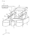
- FIG. 1 is a schematic diagram an exemplary bonding apparatus according to the invention.
- the bonding apparatus is equipped with a wafer holding stage 1 serving as a first holding unit which holds a semiconductor wafer, a sheet holding stage 2 serving as a second holding unit which holds a sheet on which a plurality of glass pieces (bond substances) are placed, and a glass resting stage 3 provided between the wafer holding stage 1 and the sheet holding stage 2 and serving as an intermediate stage on which the glasses sucked from the sheet are rested temporarily.
- a rectangular base 4 is provided whose direction of the length is parallel to the direction of the arrangement of the wafer holding stage 1, the sheet holding stage 2, and the glass resting stages 3 (the direction of the X axis shown in FIG. 1).
- a first suction device 5 is provided which sucks the glass from the sheet held on the sheet holding stage 2 and which conveys the glass to the glass resting stage 3.
- a second suction device 6 is provided which sucks the glass rested on the glass resting stage 3 and which places the glass onto the semiconductor wafer held on the wafer holding stage 1.
- the first suction device 5 has a cuboid pickup-head X-axial moving unit 5a, a cuboid pickup-head Z-axial moving unit 5b provided on a side of the pickup-head X-axial moving unit 5a, a cylindrical pickup-head Y-axial moving unit 5c provided so as to be exposed from an end surface of the pickup-head Z-axial moving unit 5b, and a pickup head 5d attached to the end of the pickup-head Y-axial moving unit 5c and serving as a suction member having a suction function.
- the pickup-head X-axial moving unit 5a is movable in the direction of the X axis
- the pickup-head Z-axial moving unit 5b is movable in the direction of the Z axis
- the pickup-head Y-axial moving unit 5c is movable in the direction of the Y axis.
- the control of the movements of these pickup-head moving units 5a, 5b, and 5c makes it possible to freely position the pickup head 5d in its three-dimensional direction.
- the second suction device 6 has a bonding head X-axial moving unit 6a movable in the direction of the X axis, a bonding head Z-axial moving unit 6b movable in the direction of the Z axis, a bonding head Y-axial moving unit 6c movable in the direction of the Y axis, and a bonding head 6d serving as a suction member capable of being freely positioned in the three-dimensional direction.
- the movements of the individual moving units are controlled by control signals from a control unit 7.
- a suction path (not shown) is formed inside, so that the glass can be sucked by vacuum suction.
- the bonding head 6d of the second suction device 6 incorporates a heater 6e having a heating function to heat the sucked glass.
- the pickup head 5d of the first suction device 5 is not provided with such a heater.
- a de-electrifying unit (ionizer) 8 which de-electrifies the glass by the first suction device 5.
- the de-electrifying unit 8 performs de-electrification process by blasting an ionized gas to the glass.
- FIG. 2 is a cross-sectional view of an exemplary semiconductor wafer 10 held on the wafer holding stage 1.
- the semiconductor wafer 10 has a structure in which a plurality of light-receiving portions 11a and microlenses 11b are patterned on one surface of a semiconductor substrate 11 and in which a plurality of bonding layers 12 are patterned in regions other than regions where the light-receiving portions 11a and the microlenses 11b are formed.
- vacuum suction can be used to hold the semiconductor wafer 10 on the wafer holding stage 1.
- the bonding layers 12 undoubtedly contain a heat-hardenable adhesive which develops adhesivity through heating.
- the layers 12 can be pattern-printed by using screen printing or the like, while in the embodiments of the invention, the bonding layers 12 are patterned in a photolithographic process (exposure and development) using a mixture of the hest-hardenable adhesive and a photosensitive adhesive (photo-hardenable adhesive) which develops adhesivity through photoirradiation so as to allow finer patterning.
- FIG. 3 is a cross-sectional view of an exemplary sheet 20 which is held on the sheet holding stage 2 and on which the glasses are placed.
- the sheet 20 has a structure in which the glasses 22 are adhered to one surface of an adhesive sheet 21.
- Such glasses 22 are fabricated by cutting a glass sheet adhered to the adhesive sheet 21 into glass pieces.
- the adhesive sheet 21 is supported by a ring-shaped frame body at its perimeter, and the ring-shaped frame body is clamp-held by the sheet holding stage 2.
- the adhesive sheet 21 it is possible to use an adhesive sheet whose adhesivity is degraded by photoirradiation such as ultraviolet irradiation.
- photoirradiation such as ultraviolet irradiation
- the glasses 22 are placed so as to cover the light receiving portions 11a shown in FIG. 2 and function as translucent coverings for a solid-state imaging device.
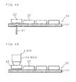
- the underside of the adhesive sheet 21 immediately underneath the glass 22 to be peeled off is pushed up with a pin 31 into a state in which the glass 22 is partly peeled from the adhesive sheet 21 (see FIG. 4A), after which the glass 22 is sucked up with the first suction device 5 (pickup head 5d) to be completely peeled from the adhesive sheet 21 (see FIG. 4B). While sucked up with the first suction device 5, the glass 22 peeled off is conveyed to the glass resting stage 3, and then the glass 22 is rested on the glass resting stage 3.
- the glass 22 becomes charged.
- the glass 22 is an electrical insulator, and there is a tendency for dust, such as glass swarf produced during the cutting of the glass sheet, to adhere to the piece of glass 22.
- the dust may become a cause of their defectiveness; hence, it is necessary to suppress the adhesion of the dust to the glass 22.
- the glass 22 sucked up with the first suction device 5 is de-electrified by the de-electrifying unit 8. Since the de-electrification processing suppresses the adhesion of the dust to the glass 22, semiconductor devices using the glasses 22 offer a significant decrease in the occurrence of defectives.
- the glass 22 rested on the glass resting stage 3 is sucked up with the second suction device 6 (bonding head 6d), and then the second suction device 6 sucking up the glass 22 is moved above the semiconductor wafer 10 on which the bonding layers 12 are patterned (see FIG. 5A).
- the glass 22 is positioned in advance for the purpose of being adhered to the semiconductor substrate 11 via the bonding layers 12, following which the second suction device 6 (bonding head 6d) descends to place the glass 22 onto the bonding layers 12.
- the suction function of the second suction device 6 (bonding head 6d) is deactivated (see FIG. 5B).
- the glass 22 is heated with the heater 6e incorporated in the second suction device 6 (bonding head 6d).
- a temperature at which the glass 22 is heated is set so that the heat-hardenable adhesive of the bonding layer 12 develops its adhesivity with heat transfer through the medium of the glass 22, which allows the glass 22 to adhere to the semiconductor substrate 11 via the bonding layer 12.
- such a heating through which the heat-hardenable adhesive of the bonding layer 12 develops its adhesivity is not conducted from the side of the semiconductor wafer 10.
- the heat is less easily transferred to the bonding layers 12 on which the glass 22 is not yet placed, so that the bonding layers 12 other than the bonding layers 12 to be adhered which have already been heated and pressurized by the second suction device 6 do not harden.
- the glasses 22 are temporarily adhered to the extent that they do not peel off in subsequent steps in view of time taken for the manufacturing process of semiconductor devices etc.
- the semiconductor wafer 10 provided with the glasses 22 adhered to the semiconductor substrate 11 is fabricated (see FIG. 5C). Since the bonding layers 12 reach a temperature at which they develops their adhesivity only when they come in contact with the glasses 22 sucked up by the second suction device 6 (bonding head 6d), the bonding (adhesion) of the individual glasses 22 can be conducted reliably.
- the semiconductor wafer 10 is removed from the wafer holding stage 1 and put into a heating apparatus (oven), following which the semiconductor wafer 10 is heated at a predetermined temperature to harden the bonding layers 12 completely (final hardening).
- the semiconductor wafer 10 thus fabricated is cut along parting lines 10a into individual pieces by using a dicing apparatus etc., thereby a semiconductor device (in this embodiment, a solid-state imaging device 41) having the semiconductor substrate 11 to which the glass 22 is bonded is fabricated (see FIG. 5D).
- a semiconductor device in this embodiment, a solid-state imaging device 41
- FIG. 6 is a schematic diagram of another exemplary bonding apparatus according to the invention.
- the bonding apparatus according to the second embodiment is provided with the same wafer holding stage 1 and sheet holding stage 2 as those described in the first embodiment but not provided with the glass resting stage 3.
- the bonding apparatus has a suction device 60 on the base 4.
- the suction device 60 has the same structure as that of the second suction device 6 described in the first embodiment; that is, the suction device 60 has a suction head X-axial moving unit 60a which is movable in the direction of the X axis, a suction head Z-axial moving unit 60b which is movable in the direction of the Z axis, a suction head Y-axial moving unit 60c which is movable in the direction of the Y axis, and a suction head 60d serving as a suction member which can be freely positioned in the three-dimensional direction and which incorporates a heater 60e.
- the suction device 60 successively conducts the two processings conducted by the first suction device 5 and the second suction device 6 described in the first embodiment; that is, the suction device 60 sucks up the glass from the sheet held on the sheet holding stage 2 and places the glass onto the semiconductor wafer held on the wafer holding stage 1.
- the three-dimensional position of the suction device 60 is controlled with the control unit 7.
- the de-electrifying unit 8 is provided above an area where the suction head 60d of the suction device 60 is movable.
- the underside of the adhesive sheet 21 immediately underneath the glass 22 to be peeled off is pushed up with the pin 31 into a state in which the glass 22 is partly peeled from the adhesive sheet 21 (see FIG. 4A), after which the glass 22 is sucked up with the suction device 60 (suction head 60d) to be completely peeled from the adhesive sheet 21 (see FIG. 4B).
- a heating step at which the heater 60e is used is not performed. This is because not only heating is not required particularly, but the adhesive sheet 21 is of low heat resistance.
- the glass 22 While the glass 22 is being conveyed to the wafer holding stage 1 with the glass 22 sucked up by the suction device 60 (suction head 60d), the glass 22 is de-electrified by the de-electrifying unit 8 as is the case with the first embodiment. Through the de-electrification process, the adhesion of dust to the glass 22 is suppressed, so that the occurrence of defectives is significantly reduced among the semiconductor devices including the glasses 22.
- the suction device 60 sucking up the glass 22 is moved to above the semiconductor wafer 10 (see FIG. 5A), and then the glass 22 is positioned in advance so as to be bonded to the semiconductor substrate 11 via the bonding layers 12, after which the suction head 60d is moved down to place the glass 22 onto the bonding layers 12, the glass 22 is pressurized, and the suction function of the suction head 60d is released (see FIG. 5B).
- the glass 22 is heated with the heater 60e incorporated in the suction device 60 (suction head 60d) instead of heating from the side of the semiconductor wafer 10.
- the bonding layer 12 is hardened into a state of tacking.
- the semiconductor wafer 10 having the semiconductor substrate 11 to which the glasses 22 are bonded is fabricated (see FIG. 5C).
- the bonding layers 12 are finally hardened with a heating apparatus, after which the semiconductor wafer 10 is cut into individual pieces, thereby semiconductor devices (in this embodiment, the solid-state imaging devices 41) are fabricated (see FIG. 5D).
- the glass resting stage 3 is not provided, and only the suction device 60 is provided, it is possible to make the bonding apparatus small when compared with that described in the first embodiment.
- the first suction device 5, the second suction device 6, and the suction device 60 have the one suction member (the pickup head 5d, the bonding head 6d, and the suction head 60d) respectively, while the individual suction devices may have a plurality of suction members; in that case, the suction members of the second suction device 6 and the suction device 60 should have a heater used for heating respectively.
- the processing of the glasses 22 can be conducted concurrently, thereby operation efficiency is improved.
- the positioning of the individual suction members to the semiconductor wafer and the sheet is conducted by the control of the three-dimensional position of the suction members through the fixation of the wafer holding stage 1, the sheet holding stage 2, and the glass resting stage 3 and through the movement of the three moving units of the individual suction devices, while the positioning may be conducted by the movement of the wafer holding stage 1, the sheet holding stage 2, and the glass resting stage 3 in one or plural directions; for instance, in FIGS. 1 and 6, it is possible to employ a structure in which the wafer holding stage 1, the sheet holding stage 2, and the glass resting stage 3 can be moved in the direction of the Y axis, and the head Y-axial moving units 5c, 6c, and 60c are fixed.
- the suction devices are provided with such a heating function, while a suction device (suction member) having no heating function may be used to place the glass onto the semiconductor wafer, and then a heating and pressure unit having no suction function may be used to heat and pressurize the glass.
- the invention is also applicable to the manufacture of any other kind of semiconductor devices, such as semiconductor memory including EPROM, so long as they are provided with a light-receiving unit having a translucent cover made of glass.
- the translucent cover described in the embodiments of the invention is made of glass, while resin material or the like may be used.
- the invention is also applicable to a case where other kinds of semiconductor devices are manufactured by using semiconductor chips instead of the glass as the bond substances.
- bonding layers containing an electrically conductive adhesive may be used to establish electric connections.
Landscapes
- Container, Conveyance, Adherence, Positioning, Of Wafer (AREA)
- Solid State Image Pick-Up Elements (AREA)
- Light Receiving Elements (AREA)
Applications Claiming Priority (2)
| Application Number | Priority Date | Filing Date | Title |
|---|---|---|---|
| JP2004186879 | 2004-06-24 | ||
| JP2004186879A JP2006013073A (ja) | 2004-06-24 | 2004-06-24 | ボンディング装置、ボンディング方法及び半導体装置の製造方法 |
Publications (2)
| Publication Number | Publication Date |
|---|---|
| EP1610359A2 true EP1610359A2 (de) | 2005-12-28 |
| EP1610359A3 EP1610359A3 (de) | 2008-03-19 |
Family
ID=34941755
Family Applications (1)
| Application Number | Title | Priority Date | Filing Date |
|---|---|---|---|
| EP05253907A Withdrawn EP1610359A3 (de) | 2004-06-24 | 2005-06-23 | Bondvorrichtung, Bondverfahren, und Verfahren zur Herstellung eines Halbleiterbauelements |
Country Status (6)
| Country | Link |
|---|---|
| US (1) | US20050284578A1 (de) |
| EP (1) | EP1610359A3 (de) |
| JP (1) | JP2006013073A (de) |
| KR (1) | KR100719329B1 (de) |
| CN (1) | CN100433246C (de) |
| TW (1) | TWI304643B (de) |
Families Citing this family (6)
| Publication number | Priority date | Publication date | Assignee | Title |
|---|---|---|---|---|
| US6982470B2 (en) * | 2002-11-27 | 2006-01-03 | Seiko Epson Corporation | Semiconductor device, method of manufacturing the same, cover for semiconductor device, and electronic equipment |
| JP4421934B2 (ja) * | 2004-04-30 | 2010-02-24 | 株式会社ルネサステクノロジ | 半導体装置の製造方法 |
| US7845543B1 (en) * | 2009-11-17 | 2010-12-07 | Asm Assembly Automation Ltd | Apparatus and method for bonding multiple dice |
| KR101387295B1 (ko) * | 2012-05-14 | 2014-04-18 | 삼성전기주식회사 | 카메라 모듈의 제조 장치 및 방법 |
| CN103626121A (zh) * | 2013-04-27 | 2014-03-12 | 苏州迪纳精密设备有限公司 | 一种阳极自动化键合设备 |
| TWI746209B (zh) * | 2020-10-15 | 2021-11-11 | 均華精密工業股份有限公司 | 生產設備及擷取器 |
Citations (3)
| Publication number | Priority date | Publication date | Assignee | Title |
|---|---|---|---|---|
| JPH03151666A (ja) | 1989-11-08 | 1991-06-27 | Nec Corp | 固体撮像装置の製造方法 |
| JPH08316496A (ja) | 1995-05-17 | 1996-11-29 | Nippondenso Co Ltd | 半導体装置の製造方法 |
| JP2000164636A (ja) | 1998-11-27 | 2000-06-16 | Matsushita Electronics Industry Corp | 半導体発光素子の実装方法及びこれに用いるボンディングツール |
Family Cites Families (28)
| Publication number | Priority date | Publication date | Assignee | Title |
|---|---|---|---|---|
| JPH0258349A (ja) * | 1988-08-24 | 1990-02-27 | Toshiba Corp | 半導体チップのピックアップ装置 |
| US5466325A (en) * | 1993-06-02 | 1995-11-14 | Nitto Denko Corporation | Resist removing method, and curable pressure-sensitive adhesive, adhesive sheets and apparatus used for the method |
| JP3447518B2 (ja) * | 1996-08-09 | 2003-09-16 | リンテック株式会社 | 接着シート貼付装置および方法 |
| US6184063B1 (en) * | 1996-11-26 | 2001-02-06 | Texas Instruments Incorporated | Method and apparatus for breaking and separating a wafer into die using a multi-radii dome |
| JP3301347B2 (ja) * | 1997-04-22 | 2002-07-15 | 松下電器産業株式会社 | 導電性ボールの搭載装置および搭載方法 |
| TW396474B (en) * | 1997-07-11 | 2000-07-01 | Hitachi Ltd | Method for forming bump bondings |
| KR100236487B1 (ko) * | 1997-10-22 | 2000-01-15 | 윤종용 | 정전기 방전 불량을 방지하기 위한 분할형 칩 흡착수단을구비하는 칩 접착 장치 |
| EP0913857B1 (de) * | 1997-10-30 | 2004-01-28 | ESEC Trading SA | Verfahren und Einrichtung für die Justierung des Bondkopfs einer Maschine für das Bonden von Halbleiterchips auf ein Trägermaterial |
| JPH11251335A (ja) * | 1998-03-04 | 1999-09-17 | Oki Electric Ind Co Ltd | 半導体素子の実装装置及びその実装方法 |
| JP2000036501A (ja) * | 1998-05-12 | 2000-02-02 | Sharp Corp | ダイボンド装置 |
| JP3971848B2 (ja) * | 1998-06-23 | 2007-09-05 | キヤノンマシナリー株式会社 | ダイボンダ |
| JP2000260827A (ja) * | 1999-03-12 | 2000-09-22 | Towa Corp | 半導体チップ実装用加熱装置及び加熱方法 |
| US6248201B1 (en) * | 1999-05-14 | 2001-06-19 | Lucent Technologies, Inc. | Apparatus and method for chip processing |
| US6355298B1 (en) * | 1999-08-23 | 2002-03-12 | Asm Assembly Automation Ltd. | Placement system apparatus and method |
| JP2001093938A (ja) * | 1999-09-20 | 2001-04-06 | Nec Kansai Ltd | 半導体装置及びその製造方法 |
| JP2002110856A (ja) * | 2000-10-03 | 2002-04-12 | Sony Corp | 半導体装置の製造方法 |
| JP4021614B2 (ja) * | 2000-12-11 | 2007-12-12 | 株式会社東芝 | 半導体素子のピックアップ用治具、半導体素子のピックアップ装置、半導体素子のピックアップ方法、半導体装置の製造方法及び半導体装置の製造装置 |
| JP4523732B2 (ja) | 2001-04-04 | 2010-08-11 | 東レエンジニアリング株式会社 | チップボンディング装置 |
| JP3881888B2 (ja) * | 2001-12-27 | 2007-02-14 | セイコーエプソン株式会社 | 光デバイスの製造方法 |
| US6773543B2 (en) * | 2002-05-07 | 2004-08-10 | Delaware Capital Formation, Inc. | Method and apparatus for the multiplexed acquisition of a bare die from a wafer |
| US20030209310A1 (en) * | 2002-05-13 | 2003-11-13 | Fuentes Anastacio C. | Apparatus, system and method to reduce wafer warpage |
| DE10222620A1 (de) * | 2002-05-17 | 2003-12-04 | Georg Rudolf Sillner | Verfahren zum Verarbeiten von elektrischen Bauteilen, insbesondere zum Verarbeiten von Halbleiterchips sowie elektrischen Bauelementen, sowie Vorrichtung zum Durchführen des Verfahrens |
| JP2004063948A (ja) | 2002-07-31 | 2004-02-26 | Kyocera Corp | フリップチップボンディング用ツール及びそれを用いたフリップチップボンディング装置 |
| US6835593B2 (en) * | 2002-08-01 | 2004-12-28 | Rohm Co., Ltd. | Method for manufacturing semiconductor device |
| KR100554628B1 (ko) * | 2002-12-03 | 2006-02-22 | 시바우라 메카트로닉스 가부시키가이샤 | 전자 부품의 본딩 장치 및 본딩 방법 |
| US20040113218A1 (en) * | 2002-12-16 | 2004-06-17 | Jachson Hsieh | Photosensitive assembly with a transparent layer and method for manufacturing the same |
| JP4187065B2 (ja) * | 2003-01-17 | 2008-11-26 | 日東電工株式会社 | 粘着テープ貼付け方法およびその装置 |
| JP4156460B2 (ja) * | 2003-07-09 | 2008-09-24 | Tdk株式会社 | ワークのピックアップ方法及びその装置、実装機 |
-
2004
- 2004-06-24 JP JP2004186879A patent/JP2006013073A/ja active Pending
-
2005
- 2005-06-23 US US11/166,742 patent/US20050284578A1/en not_active Abandoned
- 2005-06-23 EP EP05253907A patent/EP1610359A3/de not_active Withdrawn
- 2005-06-24 CN CNB2005100809159A patent/CN100433246C/zh not_active Expired - Fee Related
- 2005-06-24 TW TW094121307A patent/TWI304643B/zh not_active IP Right Cessation
- 2005-06-24 KR KR1020050054822A patent/KR100719329B1/ko not_active Expired - Fee Related
Patent Citations (3)
| Publication number | Priority date | Publication date | Assignee | Title |
|---|---|---|---|---|
| JPH03151666A (ja) | 1989-11-08 | 1991-06-27 | Nec Corp | 固体撮像装置の製造方法 |
| JPH08316496A (ja) | 1995-05-17 | 1996-11-29 | Nippondenso Co Ltd | 半導体装置の製造方法 |
| JP2000164636A (ja) | 1998-11-27 | 2000-06-16 | Matsushita Electronics Industry Corp | 半導体発光素子の実装方法及びこれに用いるボンディングツール |
Also Published As
| Publication number | Publication date |
|---|---|
| TWI304643B (en) | 2008-12-21 |
| JP2006013073A (ja) | 2006-01-12 |
| TW200603350A (en) | 2006-01-16 |
| KR100719329B1 (ko) | 2007-05-17 |
| EP1610359A3 (de) | 2008-03-19 |
| CN1713346A (zh) | 2005-12-28 |
| KR20060049686A (ko) | 2006-05-19 |
| CN100433246C (zh) | 2008-11-12 |
| US20050284578A1 (en) | 2005-12-29 |
Similar Documents
| Publication | Publication Date | Title |
|---|---|---|
| CN102034747B (zh) | 保护带剥离方法及其装置 | |
| US11373888B2 (en) | Protective member forming method and protective member forming apparatus | |
| US6176966B1 (en) | Method of die bonding electronic component and die bonding apparatus thereof | |
| US7969026B2 (en) | Flexible carrier for high volume electronic package fabrication | |
| KR20030028391A (ko) | 접착성 테이프의 박리 기구, 접착성 테이프의 박리 장치,접착성 테이프의 박리 방법, 반도체 칩의 픽업 장치,반도체 칩의 픽업 방법, 반도체 장치의 제조 방법 및반도체 장치의 제조 장치 | |
| JP2001007179A (ja) | 両面粘着シートに固定された物品の剥離方法および剥離装置 | |
| TWI800635B (zh) | 保護片材配設方法 | |
| KR102654506B1 (ko) | 웨이퍼 분리 방법 및 웨이퍼 분리 장치 | |
| CN112349605B (zh) | 保护部件形成装置 | |
| EP1610359A2 (de) | Bondvorrichtung, Bondverfahren, und Verfahren zur Herstellung eines Halbleiterbauelements | |
| TW202211351A (zh) | 晶圓的加工方法 | |
| JP2004273639A (ja) | 半導体装置の製造方法 | |
| WO2005083763A1 (ja) | ウェハの転写方法 | |
| CN114050116B (zh) | 保护部件形成装置 | |
| JP7772357B2 (ja) | 電子部品構造体の製造装置、プラズマ照射装置、および電子部品構造体の製造方法 | |
| JP2001308033A (ja) | ウエハ固定方法 | |
| JP6758508B2 (ja) | 基板処理方法及び基板処理システム | |
| JP2003124253A (ja) | ベアチップ実装方法および実装システム | |
| TW202601803A (zh) | 接合裝置及接合方法 | |
| CN107464761A (zh) | 半导体制程中的安装多个构件的方法 | |
| TWI238258B (en) | Wafer testing method | |
| CN119480688A (zh) | 半导体制造装置以及半导体装置的制造方法 | |
| KR20260045844A (ko) | 접합 장치, 접합 시스템, 및 접합 방법 | |
| JP4697014B2 (ja) | 半導体装置の製造方法および半導体製造装置。 | |
| TW202209461A (zh) | 保護構件形成裝置 |
Legal Events
| Date | Code | Title | Description |
|---|---|---|---|
| PUAI | Public reference made under article 153(3) epc to a published international application that has entered the european phase |
Free format text: ORIGINAL CODE: 0009012 |
|
| AK | Designated contracting states |
Kind code of ref document: A2 Designated state(s): AT BE BG CH CY CZ DE DK EE ES FI FR GB GR HU IE IS IT LI LT LU MC NL PL PT RO SE SI SK TR |
|
| AX | Request for extension of the european patent |
Extension state: AL BA HR LV MK YU |
|
| PUAL | Search report despatched |
Free format text: ORIGINAL CODE: 0009013 |
|
| AK | Designated contracting states |
Kind code of ref document: A3 Designated state(s): AT BE BG CH CY CZ DE DK EE ES FI FR GB GR HU IE IS IT LI LT LU MC NL PL PT RO SE SI SK TR |
|
| AX | Request for extension of the european patent |
Extension state: AL BA HR LV MK YU |
|
| AKX | Designation fees paid | ||
| REG | Reference to a national code |
Ref country code: DE Ref legal event code: 8566 |
|
| STAA | Information on the status of an ep patent application or granted ep patent |
Free format text: STATUS: THE APPLICATION IS DEEMED TO BE WITHDRAWN |
|
| 18D | Application deemed to be withdrawn |
Effective date: 20080920 |