EP1607941A1 - Magnetic recording medium, method of producing magnetic recording medium and magnetic storage apparatus - Google Patents
Magnetic recording medium, method of producing magnetic recording medium and magnetic storage apparatus Download PDFInfo
- Publication number
- EP1607941A1 EP1607941A1 EP04026515A EP04026515A EP1607941A1 EP 1607941 A1 EP1607941 A1 EP 1607941A1 EP 04026515 A EP04026515 A EP 04026515A EP 04026515 A EP04026515 A EP 04026515A EP 1607941 A1 EP1607941 A1 EP 1607941A1
- Authority
- EP
- European Patent Office
- Prior art keywords
- magnetic
- layer
- recording medium
- substrate
- magnetic recording
- Prior art date
- Legal status (The legal status is an assumption and is not a legal conclusion. Google has not performed a legal analysis and makes no representation as to the accuracy of the status listed.)
- Withdrawn
Links
- 230000005291 magnetic effect Effects 0.000 title claims abstract description 262
- 238000000034 method Methods 0.000 title claims description 24
- 238000003860 storage Methods 0.000 title claims description 22
- 239000000758 substrate Substances 0.000 claims abstract description 185
- 239000013078 crystal Substances 0.000 claims abstract description 126
- 239000000956 alloy Substances 0.000 claims abstract description 37
- 238000004544 sputter deposition Methods 0.000 claims description 70
- 230000002093 peripheral effect Effects 0.000 claims description 39
- 239000002245 particle Substances 0.000 claims description 31
- 229910045601 alloy Inorganic materials 0.000 claims description 28
- 239000011521 glass Substances 0.000 claims description 24
- 230000003628 erosive effect Effects 0.000 claims description 14
- 238000000151 deposition Methods 0.000 claims description 7
- 229910052750 molybdenum Inorganic materials 0.000 claims description 6
- 229910052796 boron Inorganic materials 0.000 claims description 4
- 125000006850 spacer group Chemical group 0.000 claims description 4
- 229910052721 tungsten Inorganic materials 0.000 claims description 4
- 229910015372 FeAl Inorganic materials 0.000 claims description 2
- 229910000943 NiAl Inorganic materials 0.000 claims description 2
- NPXOKRUENSOPAO-UHFFFAOYSA-N Raney nickel Chemical compound [Al].[Ni] NPXOKRUENSOPAO-UHFFFAOYSA-N 0.000 claims description 2
- 229910052720 vanadium Inorganic materials 0.000 claims description 2
- 239000010410 layer Substances 0.000 description 271
- 230000005415 magnetization Effects 0.000 description 35
- 101100501281 Caenorhabditis elegans emb-1 gene Proteins 0.000 description 31
- 238000005477 sputtering target Methods 0.000 description 24
- 230000008878 coupling Effects 0.000 description 22
- 238000010168 coupling process Methods 0.000 description 22
- 238000005859 coupling reaction Methods 0.000 description 22
- 238000006243 chemical reaction Methods 0.000 description 18
- 238000010586 diagram Methods 0.000 description 17
- 239000000463 material Substances 0.000 description 11
- 101150006611 emb-5 gene Proteins 0.000 description 9
- 239000010408 film Substances 0.000 description 7
- 239000000314 lubricant Substances 0.000 description 6
- 229910000531 Co alloy Inorganic materials 0.000 description 5
- 229910000929 Ru alloy Inorganic materials 0.000 description 5
- 229910000990 Ni alloy Inorganic materials 0.000 description 4
- 238000009826 distribution Methods 0.000 description 4
- 150000002500 ions Chemical class 0.000 description 4
- 229910052742 iron Inorganic materials 0.000 description 4
- 229910052759 nickel Inorganic materials 0.000 description 4
- UHOVQNZJYSORNB-UHFFFAOYSA-N Benzene Chemical group C1=CC=CC=C1 UHOVQNZJYSORNB-UHFFFAOYSA-N 0.000 description 3
- PZNSFCLAULLKQX-UHFFFAOYSA-N Boron nitride Chemical compound N#B PZNSFCLAULLKQX-UHFFFAOYSA-N 0.000 description 3
- 229910019222 CoCrPt Inorganic materials 0.000 description 3
- 229910000684 Cobalt-chrome Inorganic materials 0.000 description 3
- 229910000640 Fe alloy Inorganic materials 0.000 description 3
- 239000010952 cobalt-chrome Substances 0.000 description 3
- 125000000524 functional group Chemical group 0.000 description 3
- 230000001965 increasing effect Effects 0.000 description 3
- 238000001755 magnetron sputter deposition Methods 0.000 description 3
- 230000003746 surface roughness Effects 0.000 description 3
- 229910000838 Al alloy Inorganic materials 0.000 description 2
- 238000002441 X-ray diffraction Methods 0.000 description 2
- 239000002131 composite material Substances 0.000 description 2
- 238000010276 construction Methods 0.000 description 2
- 229910052802 copper Inorganic materials 0.000 description 2
- 230000008021 deposition Effects 0.000 description 2
- 238000010438 heat treatment Methods 0.000 description 2
- 230000001939 inductive effect Effects 0.000 description 2
- 229910052741 iridium Inorganic materials 0.000 description 2
- 239000010687 lubricating oil Substances 0.000 description 2
- 238000005259 measurement Methods 0.000 description 2
- 229910052758 niobium Inorganic materials 0.000 description 2
- 125000001997 phenyl group Chemical group [H]C1=C([H])C([H])=C(*)C([H])=C1[H] 0.000 description 2
- 239000004033 plastic Substances 0.000 description 2
- 229910052703 rhodium Inorganic materials 0.000 description 2
- 239000000725 suspension Substances 0.000 description 2
- 229910052715 tantalum Inorganic materials 0.000 description 2
- -1 Ar ions Chemical class 0.000 description 1
- OKTJSMMVPCPJKN-UHFFFAOYSA-N Carbon Chemical compound [C] OKTJSMMVPCPJKN-UHFFFAOYSA-N 0.000 description 1
- 229910000599 Cr alloy Inorganic materials 0.000 description 1
- 229910000575 Ir alloy Inorganic materials 0.000 description 1
- 239000004952 Polyamide Substances 0.000 description 1
- 229910000629 Rh alloy Inorganic materials 0.000 description 1
- 229910003481 amorphous carbon Inorganic materials 0.000 description 1
- 230000005290 antiferromagnetic effect Effects 0.000 description 1
- 238000013459 approach Methods 0.000 description 1
- 230000015572 biosynthetic process Effects 0.000 description 1
- 229910052799 carbon Inorganic materials 0.000 description 1
- 229910052804 chromium Inorganic materials 0.000 description 1
- 238000004140 cleaning Methods 0.000 description 1
- 238000007599 discharging Methods 0.000 description 1
- 230000000694 effects Effects 0.000 description 1
- 230000008020 evaporation Effects 0.000 description 1
- 238000001704 evaporation Methods 0.000 description 1
- 239000007788 liquid Substances 0.000 description 1
- 239000000696 magnetic material Substances 0.000 description 1
- 238000012423 maintenance Methods 0.000 description 1
- 229910052748 manganese Inorganic materials 0.000 description 1
- 239000000203 mixture Substances 0.000 description 1
- 238000012986 modification Methods 0.000 description 1
- 230000004048 modification Effects 0.000 description 1
- JMANVNJQNLATNU-UHFFFAOYSA-N oxalonitrile Chemical compound N#CC#N JMANVNJQNLATNU-UHFFFAOYSA-N 0.000 description 1
- 239000010702 perfluoropolyether Substances 0.000 description 1
- 239000002985 plastic film Substances 0.000 description 1
- 229920006255 plastic film Polymers 0.000 description 1
- 229910052697 platinum Inorganic materials 0.000 description 1
- 238000005498 polishing Methods 0.000 description 1
- 229920002647 polyamide Polymers 0.000 description 1
- 230000009467 reduction Effects 0.000 description 1
- 238000011160 research Methods 0.000 description 1
- 229910052707 ruthenium Inorganic materials 0.000 description 1
- 230000035945 sensitivity Effects 0.000 description 1
- 239000002356 single layer Substances 0.000 description 1
- 239000002904 solvent Substances 0.000 description 1
- 238000004528 spin coating Methods 0.000 description 1
- 230000003068 static effect Effects 0.000 description 1
- 239000013077 target material Substances 0.000 description 1
- 239000010409 thin film Substances 0.000 description 1
- 230000007704 transition Effects 0.000 description 1
- 230000005641 tunneling Effects 0.000 description 1
Images


Classifications
-
- G—PHYSICS
- G11—INFORMATION STORAGE
- G11B—INFORMATION STORAGE BASED ON RELATIVE MOVEMENT BETWEEN RECORD CARRIER AND TRANSDUCER
- G11B5/00—Recording by magnetisation or demagnetisation of a record carrier; Reproducing by magnetic means; Record carriers therefor
- G11B5/84—Processes or apparatus specially adapted for manufacturing record carriers
- G11B5/8404—Processes or apparatus specially adapted for manufacturing record carriers manufacturing base layers
-
- G—PHYSICS
- G11—INFORMATION STORAGE
- G11B—INFORMATION STORAGE BASED ON RELATIVE MOVEMENT BETWEEN RECORD CARRIER AND TRANSDUCER
- G11B5/00—Recording by magnetisation or demagnetisation of a record carrier; Reproducing by magnetic means; Record carriers therefor
- G11B5/62—Record carriers characterised by the selection of the material
- G11B5/64—Record carriers characterised by the selection of the material comprising only the magnetic material without bonding agent
- G11B5/66—Record carriers characterised by the selection of the material comprising only the magnetic material without bonding agent the record carriers consisting of several layers
- G11B5/676—Record carriers characterised by the selection of the material comprising only the magnetic material without bonding agent the record carriers consisting of several layers having magnetic layers separated by a nonmagnetic layer, e.g. antiferromagnetic layer, Cu layer or coupling layer
-
- G—PHYSICS
- G11—INFORMATION STORAGE
- G11B—INFORMATION STORAGE BASED ON RELATIVE MOVEMENT BETWEEN RECORD CARRIER AND TRANSDUCER
- G11B5/00—Recording by magnetisation or demagnetisation of a record carrier; Reproducing by magnetic means; Record carriers therefor
- G11B5/62—Record carriers characterised by the selection of the material
- G11B5/73—Base layers, i.e. all non-magnetic layers lying under a lowermost magnetic recording layer, e.g. including any non-magnetic layer in between a first magnetic recording layer and either an underlying substrate or a soft magnetic underlayer
- G11B5/7368—Non-polymeric layer under the lowermost magnetic recording layer
- G11B5/7369—Two or more non-magnetic underlayers, e.g. seed layers or barrier layers
- G11B5/737—Physical structure of underlayer, e.g. texture
-
- G—PHYSICS
- G11—INFORMATION STORAGE
- G11B—INFORMATION STORAGE BASED ON RELATIVE MOVEMENT BETWEEN RECORD CARRIER AND TRANSDUCER
- G11B5/00—Recording by magnetisation or demagnetisation of a record carrier; Reproducing by magnetic means; Record carriers therefor
- G11B5/62—Record carriers characterised by the selection of the material
- G11B5/73—Base layers, i.e. all non-magnetic layers lying under a lowermost magnetic recording layer, e.g. including any non-magnetic layer in between a first magnetic recording layer and either an underlying substrate or a soft magnetic underlayer
- G11B5/7368—Non-polymeric layer under the lowermost magnetic recording layer
- G11B5/7379—Seed layer, e.g. at least one non-magnetic layer is specifically adapted as a seed or seeding layer
-
- G—PHYSICS
- G11—INFORMATION STORAGE
- G11B—INFORMATION STORAGE BASED ON RELATIVE MOVEMENT BETWEEN RECORD CARRIER AND TRANSDUCER
- G11B5/00—Recording by magnetisation or demagnetisation of a record carrier; Reproducing by magnetic means; Record carriers therefor
- G11B5/62—Record carriers characterised by the selection of the material
- G11B5/73—Base layers, i.e. all non-magnetic layers lying under a lowermost magnetic recording layer, e.g. including any non-magnetic layer in between a first magnetic recording layer and either an underlying substrate or a soft magnetic underlayer
- G11B5/739—Magnetic recording media substrates
- G11B5/73911—Inorganic substrates
- G11B5/73921—Glass or ceramic substrates
Definitions
- the present invention generally relates to magnetic recording media, methods of producing magnetic recording media and magnetic storage apparatus, and more particularly to a magnetic recording medium for use in longitudinal magnetic recording, a method of producing such a magnetic recording medium and a magnetic storage apparatus using such a magnetic storage apparatus.
- a magnetic disk is produced by successively forming an underlayer, a magnetic layer and a protection layer on a substrate.
- NLTS non linear transition shift
- SNR non linear transition shift
- axes of easy magnetization of a CoCr alloy forming the magnetic layer become aligned in the circumferential direction, to thereby improve the coercivity and the orientation ratio (OR) in the circumferential direction.
- This technique can achieve a high recording density, but because the substrate surface is subjected to the mechanical texturing, the shape of the textured substrate surface is inherited to the surface shape of the magnetic disk.
- the surface roughness of the disk surface increases due to the mechanical texturing of the substrate surface.
- the disk surface has the increased surface roughness, it is difficult to improve the electromagnetic conversion characteristics of the magnetic disk by reducing the distance between a magnetic head and the disk surface, and there is a limit to increasing the recording density according to this approach.
- Japanese Laid-Open Patent Application No.8-7250 proposes a method of depositing a Cr underlayer and the magnetic layer with an oblique evaporation. Further, Japanese Laid-Open Patent Applications No.2002-203312 and No.2002-260218 propose methods of sputtering an underlayer at an inclination between the substrate and the underlayer.
- Japanese Laid-Open Patent Application No.8-7250 uses Cr for the underlayer that is deposited at the inclination
- the Japanese Laid-Open Patent Applications No.2002-203312 and No.2002-260218 use Cr alloys, Ni alloys and Co alloys for the seed layer that is sputtered at the inclination.
- Other materials have not been studied in these Japanese Laid-Open Patent Applications No.8-7250, No.2002-203312 and No.2002-260218.
- the incident angle of the depositing atoms is limited by a mask which partially opens in the circumferential direction, and the film thickness in the circumferential direction is made uniform by rotating the substrate.
- the incident angle of the sputtering grains is limited by a mask which opens in a vicinity of the substrate center or opens in a ring-shape at a predetermined radial position. According to such deposition or sputtering, most of the depositing or sputtering grains will not reach the substrate surface, and the productivity is poor.
- the film thickness distribution becomes such that the film thickness easily increases in the circumferential direction in the case of the Japanese Laid-Open Patent Application No.8-7250 and the film thickness easily increases in the radial direction in the case of the Japanese Laid-Open Patent Application No.2002-203312.
- the orientation distribution becomes such that deviations occur in the orientation of the axes of easy magnetization of the magnetic layer, and inconsistencies in the electromagnetic conversion characteristic of the magnetic disk increase within the same disk surface, to thereby make it difficult to further increase the recording density.
- Another and more specific object of the present invention is to provide a magnetic recording medium, a method of producing magnetic recording medium and a magnetic storage apparatus, which can improve the orientation of the axes of easy magnetization of the magnetic layer, that is, improve the circumferential orientation of the axes of easy magnetization of the magnetic layer in the case where the magnetic recording medium has a disk-shape, and improve the recording density of the magnetic recording medium.
- Still another object of the present invention is to provide a magnetic recording medium comprising a substrate having a substrate surface; a seed layer provided on the substrate surface; an underlayer provided on the underlayer; and a recording layer provided on the underlayer, wherein information is recorded in the recording layer by magnetizing the recording layer in a recording direction, and the seed layer is formed by a polycrystal of crystal grains made of an alloy material having a B2 crystal structure, and a [100] crystal orientation of the crystal grains are inclined towards one of two sides partitioned by a plane that is formed by the recording direction and a substrate normal which is normal to the substrate surface.
- the magnetic recording medium of the present invention it is possible to improve the orientation of the axes of easy magnetization of the magnetic layer and improve the recording density of the magnetic recording medium.
- a further object of the present invention is to provide a method of producing a magnetic recording medium having a recording layer that is magnetized in a recording direction to record information in the recording layer, comprising the steps of (a) forming a seed layer on a substrate surface; (b) forming an underlayer on the seed layer; and (c) forming the recording layer on the underlayer, wherein the step (a) uses a target that is made of an alloy material having a B2 crystal structure and confronts the substrate surface, and sputters, with respect to the substrate surface, crystal grains of the target from one of two sides partitioned by a first plane that is formed by the recording direction and a substrate normal which is normal to the substrate surface in a predetermined direction inclined with respect to the substrate normal.
- the method of producing the magnetic recording medium according to the present invention it is possible to improve the orientation of the axes of easy magnetization of the magnetic layer and improve the recording density of the magnetic recording medium.
- Another object of the present invention is to provide a magnetic storage apparatus comprising at least one magnetic recording medium; and a head to record and/or reproduce information to and/or from the magnetic recording medium
- the magnetic recording medium comprises a substrate having a substrate surface, a seed layer provided on the substrate surface, an underlayer provided on the underlayer, and a recording layer provided on the underlayer, information is recorded in the recording layer by magnetizing the recording layer in a recording direction, and the seed layer is formed by a polycrystal of crystal grains made of an alloy material having a B2 crystal structure, and a [100] crystal orientation of the crystal grains are inclined towards one of two sides partitioned by a plane that is formed by the recording direction and a substrate normal which is normal to the substrate surface.
- the magnetic storage apparatus of the present invention it is possible to improve the orientation of the axes of easy magnetization of the magnetic layer and improve the recording density of the magnetic recording medium.
- FIG. 1 is a cross sectional view showing an embodiment of a magnetic recording medium according to the present invention.
- a magnetic recording medium 10 shown in FIG. 1 has a disk substrate 11, and a seed layer 12, an underlayer 13, a first magnetic layer 14, a nonmagnetic coupling layer 15, a second magnetic layer 16, a protection layer 19 and a lubricant layer 20 that are successively formed on the disk substrate 11.
- the first magnetic layer 14, the nonmagnetic coupling layer 15 and the second magnetic layer 16 form a recording layer 18.
- the recording layer 18 has an exchange-coupled structure in which the first and second magnetic layers 14 and 16 are antiferromagnetically exchange-coupled via the nonmagnetic coupling layer 15. In a state where no external magnetic field is applied on the magnetic recording medium 10, magnetizations of the first and second magnetic layers 14 and 16, oriented in an in-plane direction, are mutually antiparallel.
- This embodiment is characterized by the seed layer 12.
- axes of easy magnetization of crystal grains forming the recording layer 18 are oriented in a circumferential direction of the disk substrate 11, even if no mechanical texturing is provided on the surface of the disk substrate 11 and/or the seed layer 12.
- a circumferential coercivity Hcc, an orientation Hcc/Hcr, and a circumferential coercivity squareness ratio S* of the magnetic recording medium 10 improve, where Hcr denotes a radial direction coercivity.
- the disk substrate 11 is made up of a plastic substrate, a glass substrate, a NiP-plated Al alloy substrate, a Si substrate or the like having a disk-shape.
- the surface of the disk substrate 11 may or may not be textured.
- the surface of the plastic substrate, the glass substrate or the NiP-plated Al alloy substrate may be textured by being subjected to a mechanical texturing or a laser texturing in the circumferential direction, that is, in a longitudinal direction of tracks formed on the magnetic recording medium 10.
- the seed layer 12 is made of a polycrystal having crystal grains formed by an alloy having a B2 crystal structure, such as AlRu, NiAl and FeAl.
- the seed layer 12 is formed by an inclined (or oblique) sputtering which will be described later. When the seed layer 12 is formed by the inclined sputtering, the crystal grains of the seed layer 12 grow obliquely to a normal to the substrate surface of the disk substrate 11.
- FIG. 2 is a diagram schematically showing the orientation of crystal grains in this embodiment of the magnetic recording medium.
- the crystal grains of the seed layer 12 are formed obliquely, that is, inclined towards the outer peripheral side of the disk substrate 11, where an arrow OD indicates the outer peripheral side of the disk substrate 11.
- An inclination angle ⁇ GRA of the crystal grains of the seed layer 12 with respect to a substrate normal NOR which is normal to the substrate surface is set with a range that is less than or equal to a range (from 38.7 degrees to less than 90 degrees) of the incident angle of the embodiment samples which will be described later.
- the underlayer 13, the first magnetic layer 14, the nonmagnetic coupling layer 15 and the second magnetic layer 16 that are successively formed on the seed layer 12 are formed by normal sputtering, that is, a perpendicular sputtering, such that the crystal grains are formed perpendicularly to the substrate surface.
- crystal grains 13a, 14a, 15a and 16a of the underlayer 13, the first magnetic layer 14, the nonmagnetic coupling layer 15 and the second magnetic layer 16 respectively grow in the direction of the substrate normal NOR.
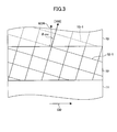
- FIG. 3 is a diagram schematically showing the orientation of crystal lattices of the crystal grains forming the seed layer 12.
- a lattice face 12-1 of the crystal lattice forming the seed layer 12 such as the (100) face, for example, is inclined from the substrate in-plane direction towards the outer peripheral side (direction OD) of the disk substrate 11.
- the inclination angle of the lattice face 12-1 may be described by an angle ⁇ CRY formed by the substrate normal NOR and the [100] crystal orientation, and this angle ⁇ CRY will be referred to as a crystal orientation inclination angle.
- the orientation of the crystal grains in the circumferential direction improves and the electromagnetic conversion characteristics improve when the crystal orientation inclination angle ⁇ CRY is set in a range from 2.1 degrees to less than 5.4 degrees.
- the crystal lattices of the seed layer 12 are formed at an inclination
- the crystal lattices of the underlayer 13 formed on the seed layer 12 are also formed at an inclination, and this inclination is inherited to the first magnetic layer 14 and the second magnetic layer 16 shown in FIGS. 1 and 2.
- the present inventor confirmed that the crystal grains having the axes of easy magnetization inclined in the radial direction have the axes of easy magnetization inclined by approximately 2.7 degrees from the in-plane direction.
- the formation of the seed layer 12 by the inclined sputtering affects the crystal orientations of the first and second magnetic layers 14 and 16.
- the phenomenon in which the axes of easy magnetization of the first and second magnetic layers 14 and 16 that are oriented in the circumferential direction of the disk substrate 11 increase probability-wise is also similarly induced by the inclination of the crystal lattices of the seed layer 12, and that orientation of the crystal grains of the first and second magnetic layers 14 and 16 in the circumferential direction is improved thereby.
- the thickness of the seed layer 12 is set in a range of 5 nm to 30 nm. From the point of view of obtaining satisfactory electromagnetic conversion characteristics of the magnetic recording medium 10, the thickness of the seed layer 12 is preferably set in a range of 5 nm to 15 nm if the surface of the disk substrate 11 or another seed layer arbitrarily provided under the seed layer 12 is mechanically textured, and is preferably set in a range of 5 nm to 25 nm if no mechanical texturing is applied to the surface of the disk substrate 11 or the other seed layer arbitrarily provided under the seed layer 12.
- a layer made of a material similar to that used for the seed layer 12 may be formed directly on the seed layer 12 by perpendicular sputtering.
- this layer has crystal grains thereof grown in the direction of the substrate normal NOR, and has a thickness in a range of 5 nm to 30 nm. Crystal lattices of this layer are inclined by inheriting the inclination of the crystal lattices of the seed layer 12 provided underneath, and effects similar to those obtained by performing the inclined sputtering are obtainable, to thereby enable the thickness of the seed layer 12 to be reduced.
- the underlayer 13 may be made up of a stacked structure that includes a plurality of stacked layers made of Cr or the Cr-X alloy. By using the stacked structure for the underlayer 13, it is possible to suppress the crystal grains of the underlayer 13 from becoming large, and to suppress the crystal grains of the first and second magnetic layers 14 and 16 from becoming large.
- the first magnetic layer 14 has a thickness in a range of 0.5 nm to 20 nm, and is made of Co, Ni, Fe, Co alloy, Ni alloy, Fe alloy or the like, for example.
- the first magnetic layer 14 may be made up of a stacked structure that includes a plurality of stacked layers made of Co, Ni, Fe, Co alloy, Ni alloy, Fe alloy or the like. By using the stacked structure for the first magnetic layer 14, it is possible to improve the orientation of the crystal grains of the second magnetic layer 16.
- the Ru alloy may include at least one of Co, Cr, Fe, Ni, Mn or alloys thereof.
- the thickness of the nonmagnetic coupling layer 15 is in a range of 0.4 nm to 1.5 nm, and preferably in a range of 0.6 nm to 0.9 nm. Depending on the Ru-content within the Ru alloy in the case of the nonmagnetic coupling layer 15 made of the Ru alloy, the thickness of the nonmagnetic coupling layer 15 may be in a range of 0.8 nm to 1.4 nm.
- the first and second magnetic layers 14 and 16 are exchange-coupled via the nonmagnetic coupling layer 15, and by setting the thickness of the nonmagnetic coupling layer 15 within the above described range, the first and second magnetic layers 14 and 16 become antiferromagnetically coupled.
- magnetizations of the first and second magnetic layers 14 and 16 become mutually antiparallel as indicated arrows in FIG. 1.
- the exchange coupling state of the first and second magnetic layers 14 and 16 depends on the thickness of the nonmagnetic coupling layer 15, and the magnetizations of the first and second magnetic layers 14 and 16 reciprocate between the mutually antiparallel state and a mutually parallel state depending on the thickness of the nonmagnetic coupling layer 15.
- the thickness of the nonmagnetic coupling layer 15 is particularly preferable to set the thickness of the nonmagnetic coupling layer 15 to match a first antiferromagnetic peak where the magnetizations of the first and second magnetic layers 14 and 16 become mutually antiparallel and the thickness of the nonmagnetic coupling layer 15 is the thinnest.
- the second magnetic layer 16 has a thickness in a range of 5 nm to 20 nm, and is made of Co, Ni, Fe, Co alloy, Ni alloy, Fe alloy and the like, similarly as in the case of the first magnetic layer 14. It is preferable that a product of a remanent magnetization Mr1 and a thickness t1 of the first magnetic layer 14 (that is, a remanent magnetization and thickness product Mr1 x t1) and a product of a remanent magnetization Mr2 and a thickness t2 of the second magnetic layer 16 (that is, a remanent magnetization and thickness product Mr2 x t2) satisfy a relationship (Mr1 x t1) ⁇ (Mr2 x t2).
- the second magnetic layer 16 has the magnetization in the same direction as the total remanent magnetization of the magnetic recording medium 10, and information can be written accurately in the second magnetic layer 16 in correspondence with switching positions of the recording magnetic field of the magnetic head.
- the remanent magnetization and thickness product Mr1 x t1 and the remanent magnetization and thickness product Mr2 x t2 may satisfy a relationship (Mr1 x t1) > (Mr2 x t2).
- the first magnetic layer 14 and the second magnetic layer 16 may have different compositions.
- the material used for the second magnetic layer 16 is selected from materials which result in a larger anisotropic magnetic field than the material used for the first magnetic layer 14.
- the alloy used for the second magnetic layer 16 may be added with Pt while no Pt is added for the alloy used for the first magnetic layer 16 or, the Pt-content (in atomic percent) of the alloy may be larger for the second magnetic layer 16 than the first magnetic layer 14.
- the Pt-content (in atomic percent) of the alloy may be larger for the second magnetic layer 16 than the first magnetic layer 14.
- CoCrPt 8 may be used for the first magnetic layer 14 and CoCrPt 12 may be used for the second magnetic layer 16, where the numeral affixed to Pt denotes atomic percent (at.%). The atomic percent (at.%) of other elements are indicated similarly in this specification.
- the first and second magnetic layers 14 and 16 are antiferromagnetically exchange-coupled via the nonmagnetic coupling layer 15.
- the apparent volume of the recording layer 18 becomes substantially equal to a sum of the volumes of the first and second magnetic layers 14 and 16, which is large compared to the case where the recording layer is formed by a single-layer structure, to thereby improve the thermal stability of the magnetizations (or written bits).
- the recording layer 18 may be formed by a stacked structure having more than 2 magnetic layers.
- the magnetic layers of the stacked structure are exchange-coupled, and at least two magnetic layers are antiferromagnetically exchange-coupled.
- the recording layer 18 may be formed by a single magnetic layer which does not employ the exchange coupling, similarly as in the case of the conventional magnetic recording media.
- the protection layer 19 has a thickness in a range of 0.5 nm to 10 nm, and preferably in a range of 0.5 nm to 5 nm, and is made of Diamond-Like Carbon (DLC), carbon nitride, amorphous carbon and the like, for example.
- DLC Diamond-Like Carbon
- the lubricant layer 20 is made of an organic liquid lubricant having perfluoropolyether as a main chain and -OH, phenyl, benzene ring or the like as the terminal functional group. More particularly, ZDol manufactured by Monte Fluos (terminal functional group: -OH), AM3001 manufactured by Ausimonoto (terminal functional group: benzene ring), Z25 manufactured by Monte Fluos, and the like, with a thickness in a range of 0. 5 nm to 3.0 nm, may be used for the lubricant layer 20.
- the lubricant may be appropriately selected depending on the material used for the protection layer 19. Depending on the kind of protection layer 19 used, the lubricant layer 20 may be omitted.
- This other seed layer may be made of a nonmagnetic material such as NiP, CoW and CrTi.
- the surface of this other seed layer may or may not be textured.
- an amorphous material such as NiP it is preferable that the surface of this other seed layer is oxidized.
- This other seed layer made of NiP that is preferably oxidized, improves the c-axis in-plane orientation of the first and second magnetic layers 14 and 16.
- suitable materials other than NiP may be used to improve the c-axis orientation of the first and second magnetic layers 14 and 16.
- a nonmagnetic intermediate layer (not shown) may be provided between the underlayer 13 and the first magnetic layer 14.
- the nonmagnetic intermediate layer grows by inheriting the crystallinity and crystal grain size of the underlayer 13, and improves the crystallinity of the first and second magnetic layers 14 and 16 which are epitaxially grown above the nonmagnetic intermediate layer.
- the nonmagnetic intermediate layer reduces the grain size deviation width in the distribution of the crystal grain (magnetic grain) sizes, and promotes the orientation of the c-axis in the in-plane direction.
- the nonmagnetic intermediate layer may be formed by a stacked structure that is made up of a plurality of layers made of the nonmagnetic alloys described above, and in this case, it is possible to further improve the crystal orientations of the first and second magnetic layers 14 and 16.
- the lattice constant of the nonmagnetic intermediate layer may be set to differ by several % with respect to the lattice constant of the first magnetic layer 14 or the second magnetic layer 16, so as to generate an internal stress in the in-plane direction at the interface of the nonmagnetic intermediate layer and the first magnetic layer 14 or, within the first magnetic layer 14, so as to increase the coercivity of the first magnetic layer 14.
- the seed layer 12 is formed by a polycrystal of crystal grains made of an alloy material having a B2 crystal structure, and a [100] crystal orientation of the crystal grains are inclined towards one of two sides partitioned by a plane that is formed by the recording direction and substrate normal NOR which is normal to the substrate surface.
- the B2 crystal structure has atoms A and atoms B of an alloy AB arranged alternately at the adjacent atomic sites of the bcc crystal structure.
- the seed layer 12 is deposited so that the [100] crystal orientation of the crystal lattices forming the seed layer 12 is inclined towards the outer peripheral side of the disk substrate 11 relative to the substrate normal NOR.
- the crystal orientation of the recording layer 18 in the circumferential direction is improved, to thereby improve the static magnetic characteristics and the electromagnetic conversion characteristics, and as a result, it is possible to increase the recording density of the magnetic recording medium 10 and realize a high recording density.
- the [100] crystal orientation includes the [010] crystal orientation and the [001] crystal orientation that are equivalent to the [100]crystal orientation.
- the [100] crystal orientation indicates the [100] crystal orientation or a crystal orientation that has a smallest angle relative to the substrate normal NOR.
- the crystal orientation of the second magnetic layer 16 can be improved without providing the mechanical texturing on the substrate surface or the like.
- the surface smoothness of the magnetic recording medium 10 is improved, to thereby enable reduction in the spacing between the recording element and/or the reproducing element and the recording layer 18, and the recording density of a magnetic storage apparatus which uses the magnetic recording medium 10 can further be improved.
- FIGS. 4A through 4C are cross sectional views for explaining an embodiment of the method of producing the magnetic recording medium according to the present invention.
- the disk substrate 11 is heated to 180°C within a vacuum atmosphere by use of a pyrolytic boron nitride (PBN) heater, for example.
- PBN pyrolytic boron nitride
- a sputtering apparatus is used to form the seed layer 12 on the substrate surface of the disk substrate 11 by the inclined sputtering.
- the inside of the chamber is once exhausted to a vacuum of 10 -5 Pa or less, and an Ar gas pressure is set to 0.67 Pa and the power is set to 2 kW, so as to form the seed layer 12 to a thickness of 10 nm by the D.C. magnetron sputtering with a discharge time of 4 seconds, for example.
- the inclined sputtering which forms an important part of this embodiment, is carried out in the following manner.
- FIG. 5 is a perspective view generally showing an important part of the sputtering apparatus.
- FIG. 5 shows the inside of a chamber (not shown) of a sputtering apparatus 30.
- a circular sputtering target 31 made of a material having a B2 crystal structure, such as an AlRu alloy, is arranged so that a sputtering surface of the sputtering target 31 confronts the substrate surface of the disk substrate 11.
- a magnet unit 32 is arranged on a rear of the sputtering target 31.
- a rotary shield part 33 is arranged between the disk substrate 11 and the sputtering target 31.
- the sputtering apparatus 30 further includes an exhaust system for exhausting the inside of the chamber, a gas introducing system for introducing gasses into the chamber, and a power supply for supplying discharging power to the sputtering target 31.
- the sputtering apparatus 30 traps discharge plasma including electrons and gas ions, such as Ar ions, in a vicinity of the sputtering surface of the sputtering target 31, along the lines of magnetic force of the magnet unit 32.
- the Ar ions cause the target material at a predetermined region on the target surface of the sputtering target 31 to be sputtered onto the substrate surface of the disk substrate 11 as sputtered particles.
- the sputtered particles move approximately linearly from the sputtering target 31 towards the substrate surface to form the seed layer 12.
- An erosion region 31a is formed in the predetermined region of the target surface of the sputtering target 31 where the sputtering particles originated.
- the rotary shield part 33 has a rotary shaft 33a provided coaxially to the disk substrate 11, the sputtering target 31 and the magnet unit 32.
- the rotary shield part 33 also has a plurality of shield plates 33b that extend radially outwards from the rotary shaft 33a. Surfaces of the shield plates 33b are perpendicular to the target surface of the sputtering target 31.
- the shield plates 33b are arranged at equal angular intervals around the rotary shaft 33a.
- a length of each shield plate 33b in the radial direction, from the center of the rotary shaft 33a to the outer peripheral edge of the shield plate 33b, is approximately the same as or is greater than the radius of the disk substrate 11.
- the sputtering particles moving in the radial direction of the disk substrate 11 reach the substrate surface of the disk substrate 11 more easily than the sputtering particles moving in the circumferential direction of the disk substrate 11, so as to suppress the sputtering particles from moving in a direction away from the radial direction to become deposited with an inclination on the substrate surface.
- the arrangement and dimensions of the shield plates 33b also prevent the sputtering particles from passing the central portion of the disk substrate 11 to become deposited on the opposite surface of the disk substrate 11. Accordingly, crystal grains having small deviations in the growth direction are grown on the substrate surface of the disk substrate 11 to form the seed layer 12.
- each shield plate 33b in the radial direction may be smaller than the radius of the disk substrate 11. In this case, it is still possible to prevent the sputtering particles from passing the central portion of the disk substrate 11 to become deposited on the opposite surface of the disk substrate 11.
- the rotary shaft 33a of the rotary shield part 33 is connected to a rotary driving part 34 (shown in FIG. 6 which will be described later) that is provided on the rear of the sputtering target 31, and the rotary shield part 33 is rotated by the rotary driving part 34 at a rotational speed of 60 rpm, for example.
- a rotary driving part 34 shown in FIG. 6 which will be described later
- the rotary shield part 33 is rotated by the rotary driving part 34 at a rotational speed of 60 rpm, for example.
- the rotary shield part 33 does not necessarily have to be rotated.
- FIG. 6 is a cross sectional view showing an important part of the sputtering apparatus 30 shown in FIG. 5.
- FIG. 6 is a cross sectional view cut along a plane passing a center axis Ax which approximately matches the center axes of the disk substrate 11, the sputtering target 31 and the magnet unit 32 shown in FIG. 5. Since the structures above and below the center axis Ax are symmetrical about the center axis Ax, only the upper structure is shown in FIG. 6.
- the magnet unit 32 includes a magnet base 32a and a magnet part 32b.
- the magnet part 32b is made up of an outer ring-shaped magnet 35, an inner ring-shaped magnet 36 and a yoke 38.
- the outer and inner ring-shaped magnets 35 and 36 are formed by permanent magnets that are magnetized in the direction of the arrows shown in FIG. 6.
- the yoke 38 is made of a soft magnetic material.
- Lines of magnetic force (hereinafter simply referred to as lines MF) of the magnet part 32b extend from the N-pole of the inner ring-shaped magnet 36, pass through the sputtering target 31, turn and pass through the sputtering target 31 again, and return to the S-pole of the outer ring-shaped magnet 35.
- Ar ions forming the discharge plasma trapped along the lines MF cause the sputtering particles to be discharged from the sputtering surface of the sputtering target 31, and cause the erosion region 31a to be formed on the sp
- the outer and inner ring-shaped magnets 35 and 36 may be formed by electromagnets.
- the magnet part 32b is arranged so that the erosion region 31a of the sputtering target 31 is located on the outer side of the outer peripheral side of the disk substrate 11, to cause the sputtering particles to move towards the disk substrate 11 at an inclination from the outer peripheral side to the inner peripheral side, that is, to cause the sputtering particles to become incident to the substrate surface at an inclination angle ⁇ INC .
- the inclination angle ⁇ INC of the sputtering particles with respect to the disk substrate 11 is preferably set in a range of 38.7 degrees to less than 90 degrees. By setting the inclination angle ⁇ INC in this range, the crystal orientation inclination angle ⁇ CRY shown in FIG.
- the substrate normal NOR and the [100] crystal orientation of the seed layer 12 that is formed can be set in a rage of 2.1 degrees to less than 5.4 degrees. As a result, it is possible to improve the crystal orientation of the recording layer 18 in the circumferential direction of the disk substrate 11, as may be seen from the embodiment samples which will be described later.
- the inclination angle ⁇ INC is preferably set in a range of 38.7 degrees to 80 degrees or less, and more preferably in a range of 38.7 degrees to 75 degrees or less. Furthermore, from the point of view of further improving the crystal orientation of the recording layer 18 in the circumferential direction of the disk substrate 11, the inclination angle ⁇ INC is preferably set in a range of 43.0 degrees to 75 degrees or less.
- the upper limit of the crystal orientation inclination angle ⁇ CRY is based on the fact that the crystal orientation inclination angle ⁇ CRY is approximately 6% of the inclination angle ⁇ INC from the second and third embodiment samples which will be described later.
- the inclination angle ⁇ INC is defined as an angle formed between the substrate normal NOR and an imaginary incident line that connects a center T ERO of the erosion region 31a and a depositing position in a track region on the substrate surface of the disk substrate 11.
- the track region is defined as the region between an inner (or innermost) peripheral position D IN and an outer (or outermost) peripheral position D OUT .
- the center T ERO of the erosion region 31a is defined as an intersection of the sputtering surface of the sputtering target 31 before the sputtering starts and a bisector 35ac between a centerline 35c of the outer ring-shaped magnet 35 and a centerline 36c of the inner ring-shaped magnet 36.
- the shield plates 33b are provided in the vicinity of the center axis Ax, the sputtering particles moving in the radial direction of the disk substrate 11 so as to pass beyond the center axis Ax will be blocked by the shield plates 33b. Hence, such sputtering particles adhere on the shield plates 33b and are prevented from passing beyond the center axis Ax and reaching the disk substrate 11.
- the seed layer 12 that is formed on the substrate surface of the disk substrate 11 is substantially formed by the crystal grains that are inclined towards the outer peripheral side of the disk substrate 11 in the radial direction, and the crystal grain orientation of the seed layer 12 is approximately uniform. For this reason, the crystallinity of the seed layer 12 improves and the inclination of the crystal lattices of the seed layer 12 becomes approximately uniform, to thereby suppress locally non-uniform in-plane crystal orientation of the recording layer 18.
- the underlayer 13, the first magnetic layer 14, the nonmagnetic coupling layer 15 and the second magnetic layer 16 which are made of the materials described above are successively formed on the seed layer 12 by sputtering.
- the layers 13 through 16 are formed by setting the Ar gas pressure to 0.67 Pa and successively sputtering the layers 13 through 16 by the D.C. magnetron sputtering so that the sputtering particles reach the substrate surface of the disk substrate 11 at an incident angle that is approximately perpendicular to the substrate surface.
- the disk substrate 11 may be heated again before forming the first magnetic layer 14 or the nonmagnetic coupling layer 15.
- the heating temperature of the disk substrate 11 in this case is set to 270°C or less, and preferably in a range of 200°C to 240°C.
- the protection layer 19 made of DLC or the like is formed on the second magnetic layer 16 to a thickness of 3 nm, for example, by sputtering, CVD, FCA or the like.
- the steps from the substrate heating step shown in FIG. 4A to the protection layer forming step shown in FIG. 4C are carried out within the chamber.
- the disk substrate 11 is not exposed to the outside even during transport while each of these steps are carried out.
- the step shown in FIG. 4C may use an organic liquid lubricant that is diluted by a fluoric solvent or the like, and the lubricant layer 20 may be formed to a thickness of 1.5 nm, for example, by pulling, spin-coating, liquid submersion, steam jet and the like.
- the magnetic recording medium 10 is created in this manner by the above described steps.
- the erosion region 31a of the sputtering target 31 is located on the outer side of the outer peripheral side of the disk substrate 11, to cause the sputtering particles to move towards the disk substrate 11 at an inclination from the outer peripheral side to the inner peripheral side, that is, to cause the sputtering particles to become incident to the substrate surface at the inclination angle ⁇ INC with respect to the substrate normal NOR.
- the inclination angle of the crystal grains of the seed layer 12 from becoming non-uniform, and to suppress the [100] crystal orientation of the crystal grains of the seed layer 12 from becoming non-uniform. Therefore, the crystal orientation of the recording layer 18 in the circumferential direction of the disk substrate 11 is improved, and it is possible to increase the recording density of the magnetic recording medium 10.
- the rotary shield part 33 is provided between the disk substrate 11 and the sputtering target 31.
- the sputtering particles from passing the central portion and/or the outer peripheral portion of the disk substrate 11 to become deposited on the opposite surface of the disk substrate 11. Consequently, it is possible to prevent the crystal grains of the seed layer 12 from inclining towards the circumferential direction or the inner peripheral side of the disk substrate 11, to further suppress the inclination angle of the crystal grains of the seed layer 12 from becoming non-uniform. Therefore, it is possible to suppress the [100] crystal orientation of the crystal grains of the seed layer 12 from becoming non-uniform, and the crystal orientation of the recording layer 18 in the circumferential direction of the disk substrate 11 is improved.
- embodiment samples created by this embodiment (hereinafter referred to as embodiment samples).
- the D.C. magnetron sputtering apparatus 30 was used to form a magnetic disk having the following structure, as the magnetic recording medium 10.
- the magnetic disk created includes a glass substrate 11 having a diameter of 65 mm, an AlRu seed layer 12 having a thickness of 10 nm, a Cr underlayer 13 having a thickness of 4.5 nm, a Co 90 Cr 10 first magnetic layer 14 having a thickness of 2 nm, a Ru nonmagnetic spacer layer 15 having a thickness of 0.7 nm, a CoCrPt 12 B 7 Cu 4 second magnetic layer 16 having a thickness of 15 nm, and a C protection layer 19 having a thickness of 4.5 nm.
- the glass substrate 11 was heated to 180°C within vacuum by the PBN heater prior to forming the AlRu seed layer 12.
- the glass substrate 11 was heated similarly to 230°C prior to forming the Ru nonmagnetic spacer layer 15.
- the erosion region 31a was formed in the AlRu sputtering target 31 between a position where the radius is 67.0 mm and a position where the radius is 77.0 mm from the disk center of the glass substrate 11.
- a center position of the erosion region 31a is located at a radius of 72.0 mm from the disk center of the glass substrate 11.
- the incident angle ⁇ INC of the sputtering particles from the outer peripheral side of the glass substrate 11 was set to a center incident angle of 46.4 degrees (of a range from 42.8 degrees to 49.6 degrees) at the outer (or outermost) peripheral position D OUT shown in FIG. 6, and to a center incident angle of 56.3 degrees (of a range from 54.0 degrees to 58.4 degrees) at the inner (or innermost) peripheral position D IN shown in FIG. 6.
- the outer (or outermost) and inner (or innermost) peripheral positions D OUT and D IN are respectively located at radii of 30 mm and 12 mm from the disk center of the glass substrate 11.
- the AlRu seed layer 12 was formed in an Ar gas with an Ar gas pressure of 0.67 Pa.
- the shield plates 33b of the rotary shield part 33 were provided at an angular interval of 30 degrees along the circumferential direction of the glass substrate 11, and the rotary shield part 31 was rotated at 60 rpm.
- the erosion region 31a was formed in the AlRu sputtering target 31 between a position where the radius is 47.0 mm and a position where the radius is 77.0 mm from the disk center of the glass substrate 11.
- a center position of the erosion region 31a is located at a radius of 62.0 mm from the disk center of the glass substrate 11.
- the incident angle ⁇ INC of the sputtering particles from the outer peripheral side of the glass substrate 11 was set to a center incident angle of 38.7 degrees (of a range from 23.0 degrees to 49.6 degrees) at the outer (or outermost) peripheral position D OUT shown in FIG.
- the second embodiment sample Emb-2 was created under the same conditions as the first embodiment sample Emb-1 described above.
- the erosion region 31a was formed in the AlRu sputtering target 31 between a position where the radius is 47.0 mm and a position where the radius is 57.0 mm from the disk center of the glass substrate 11.
- a center position of the erosion region 31a is located at a radius of 52.0 mm from the disk center of the glass substrate 11.
- the incident angle ⁇ INC of the sputtering particles from the outer peripheral side of the glass substrate 11 was set to a center incident angle of 28.8 degrees (of a range from 23.0 degrees to 34.0 degrees) at the outer (or outermost) peripheral position D OUT shown in FIG.
- the third embodiment sample Emb-3 was created under the same conditions as the first embodiment sample Emb-1 described above.
- the erosion region 31a of the AlRu sputtering target 31 was set to a position approximately confronting the glass substrate 11.
- the incident angle ⁇ INC of the sputtering particles from the outer peripheral side of the glass substrate 11 was set to 0. No rotary shield part 33 was used. Otherwise, the first comparison example Cmp-1 was created under the same conditions as the first embodiment sample Emb-1 described above.
- the crystal orientation inclination angle ⁇ CRY of the crystal lattices of the AlRu seed layer 12 was obtained for each of the first and second embodiment samples Emb-1 and Emb-2 and the first comparison example Cmp-1.
- FIG. 7 is a diagram showing rocking curves of the AlRu seed layers 12 of first and second embodiment samples Emb-1 and Emb-2 and the first comparison example Cmp-1.
- FIG. 8 is a diagram showing a relationship of the incident angles ⁇ INC of AlRu seed layers 12 and crystal orientation inclination angles ⁇ CRY of the first and second embodiment samples Emb-1 and Emb-2 and the first comparison example Cmp-1.
- Cu-K ⁇ ray X-ray diffractometer
- the (100) face is inclined by the scan angle ⁇ towards the outer peripheral side of the magnetic disk, that is, the [100] crystal orientation is inclined by the scan angle ⁇ (crystal orientation inclination angle ⁇ CRY ) from the substrate normal NOR towards the outer peripheral side of the magnetic disk.
- the layers above the AlRu seed layer 12, namely, the Co underlayer 13 up to the protection layer 19 were not formed on the magnetic disks in order to reduce noise in the rocking curves, and the thickness of the AlRu seed layer 12 was set to 100 nm.
- the peak of the rocking curve appears when the scan angle ⁇ is approximately 0.1 degrees for the first comparison example Cmp-1 which employs the perpendicular sputtering with the incident angle ⁇ INC of 0.
- the peak of the rocking curve appears when the scan angle ⁇ is -3.6 degrees for the first embodiment sample Emb-1 which employs the inclined sputtering with the incident angle ⁇ INC of 56.3 degrees (at the measured radius of 12 mm).
- the crystal orientation inclination angle ⁇ CRY of the AlRu seed layer 12 is approximately 6% of the incident angle ⁇ INC of the sputtering particles for both the first and second embodiment samples Emb-1 and Emb-2.
- FIG. 9 is a diagram showing rocking curves of the CoCrPt 12 B 7 Cu 4 second magnetic layers 16 of the first embodiment sample Emb-1 and the first comparison example Cmp-1.
- the results of FIG. 9 were obtained by measuring the rocking curves for the (110) face of the CoCrPt 12 B 7 Cu 4 second magnetic layers 16 of the first embodiment sample Emb-1 and the first comparison example Cmp-1, similarly to obtaining the results shown in FIG. 7.
- the (110) face of the CoCrPt 12 B 7 Cu 4 second magnetic layer 16 is inclined towards the outer peripheral side of the magnetic disk by an angle corresponding to the scan angle ⁇ .
- the peak of the rocking curve appears when the scan angle ⁇ is approximately 0 and the (110) face of the CoCrPt 12 B 7 Cu 4 second magnetic layer 16 is not inclined for the first comparison example Cmp-1.
- the peak of the rocking curve appears when the scan angle ⁇ is -2.7 degrees and the (110) face of the crystal grains of the CoCrPt 12 B 7 Cu 4 second magnetic layer 16, having the c-axis or the axis of easy magnetization arranged in the radial direction of the magnetic disk, is inclined towards the outer peripheral side of the magnetic disk for the first embodiment sample Emb-1.
- the scan angle ⁇ of -2.7 degrees at which the rocking curve has the peak for the CoCrPt 12 B 7 Cu 4 second magnetic layer 16 matches the scan angle ⁇ of -2.7 degrees at which the rocking curve has the peak for the AlRu seed layer 12 in FIGS. 7 and 8, for the first embodiment sample Emb-1.
- the inclination of the (100) face of the AlRu seed layer 12 is inherited to the Cr under layer 13, the Co 90 Cr 10 first magnetic layer 14 and the Ru nonmagnetic coupling layer 15, to thereby incline the (110) face of the CoCrPt 12 B 7 Cu 4 second magnetic layer 16.
- FIG. 10 is a diagram showing magnetic characteristics of magnetic disks according to the first through third embodiment samples Emb-1 through Emb-3 and the first comparison example Cmp-1.
- the magnetic characteristics of the second magnetic layer 16 were obtained using a vibration sample type magnetometer, by applying magnetic fields in the circumferential direction and the radial direction of the magnetic disks and measuring the corresponding hysteresis loops, to obtain a circumferential coercivity Hcc, an orientation Hcc/Hcr, and a circumferential coercivity squareness ratio S*, where Hcr denotes a radial direction coercivity.
- the axis of easy magnetization (or c-axis) of the second magnetic layer 16 is isotropically oriented in-plane. It may be seen from FIG. 10 that the larger the orientation Hcc/Hcr, the more the orientation of the axis of easy magnetization in the circumferential direction is promoted. It may also be seen from FIG. 10 that the larger the circumferential coercivity squareness ratio S*, the more the orientation of the axis of easy magnetization in the circumferential direction is promoted.
- the orientation Hcc/Hcr for the first comparison example Cmp-1 is 1.00, which means that the crystal grains of the second magnetic layer 16 is isotropically oriented.
- the orientation Hcc/Hcr for the first embodiment sample Emb-1 is 1.04 at the measured radius of 12 mm and 1.03 at the measured radius of 30 mm, which means that the orientation of the axis of easy magnetization of the second magnetic layer 16 in the circumferential direction is promoted.
- the circumferential coercivity squareness ratio S* is also improved for the first embodiment sample Emb-1 when compared to the first comparison example Cmp-1, and it may also be seen from the circumferential coercivity squareness ratio S* that the orientation of the axis of easy magnetization of the second magnetic layer 16 in the circumferential direction is promoted for the first embodiment sample Emb-1.
- the third embodiment sample Emb-3 employs the inclined sputtering with the incident angle ⁇ INC of 45.0 degrees at the measured radius of 12 mm and 28.8 at the measured radius of 30 mm. Otherwise, the third embodiment sample Emb-3 was created under the same conditions as the first and second embodiment samples Emb-1 and Emb-2.
- the electromagnetic conversion characteristics improve when the orientation Hcc/Hcr exceeds 1.00 of the first comparison example Cmp-1, that is, greater than or equal to 1.01. From the relationships of the inclination angle ⁇ INC and the orientation Hcc/Hcr for the first through third embodiment samples Emb-1 through Emb-3, it may be seen that the orientation Hcc/Hcr becomes 1.01 when the inclination angle ⁇ INC is 38.7 degrees (at the measured radius of 30 mm for the second embodiment sample Emb-2), and that the inclination angle ⁇ INC is preferably set to 38.7 degrees or greater. The present inventor has confirmed through studies that the electromagnetic conversion characteristic greatly improve when the orientation Hcc/Hcr is 1.02 or greater.
- the inclination angle ⁇ INC is 43.0 degrees (at the measured radius of 30 mm for the first embodiment sample Emb-1) when the orientation Hcc/Hcr becomes 1.02
- the inclination angle ⁇ INC is more preferably set to 43.0 or greater.
- the crystal orientation inclination angle ⁇ CRY of the AlRu seed layer 12 that is formed is 2.1 degrees when the inclination angle ⁇ INC is 38.7 degrees.
- the crystal orientation inclination angle ⁇ CRY is preferably set to 2.1 degrees or greater, and more preferably set to 2.7 degrees or greater which is the crystal orientation inclination angle ⁇ CRY for the case where the inclination angle ⁇ INC is 43.0.
- FIGS. 11A and 11B are diagrams showing the electromagnetic conversion characteristics of magnetic disks according to the first and second embodiment samples Emb-1 and Emb-2 and the first comparison example Cmp-1.
- the electromagnetic conversion characteristics shown in FIG. 11A and 11B were obtained using a composite magnetic head which includes an inductive recording element and a Giant Magneto-Resistive (GMR) reproducing element, to measure the isolated wave output, the resolution and the SNR.
- the isolated wave output ( ⁇ V p-p ) indicates an output average at a linear recording density of 104 kFCI.
- the resolution (%) is obtained from (average output at 104 kFCI)/(average output at 414 kFCI) x 100, and the SNR (dB) was obtained from 20 x log(S/N) based on the average output S ( ⁇ V p-p ) at 414 kFCI and the medium noise N ( ⁇ V rms ).
- FIG. 11A It may be seen from FIG. 11A that the resolution and the SNR of the first and second embodiment samples Emb-1 and Emb-2 at the measured radius of 30 mm are improved compared to the first comparison example Cmp-1.
- the orientation Hcc/Hcr of the first and second embodiment samples Emb-1 and Emb-2 are improved compared to the first comparison example Cmp-1.
- the improved orientation Hcc/Hcr improves the resolution and the SNR of the first and second embodiment samples Emb-1 and Emb-2.
- the first and second embodiment samples Emb-1 and Emb-2 are compared, it may be seen that the first embodiment sample Emb-1 which has a larger orientation Hcc/Hcr than the second embodiment sample Emb-2 has the resolution and the SNR that are improved compared to those of the second embodiment sample Emb-2. Therefore, it was confirmed that the larger the inclination angle ⁇ INC , that is, the larger the crystal orientation inclination angle ⁇ CRY , the more the resolution and the SNR are improved.
- the fourth embodiment sample Emb-4 was created similarly to the first embodiment sample Emb-1 described above, except that the substrate surface of the glass substrate 11 was subjected to a mechanical texturing using a polishing and cleaning apparatus, so as to provide the texturing in the circumferential direction of the magnetic disk with an average surface roughness Ra of 0.3 nm.
- the fifth embodiment sample Emb-5 was created similarly to the second embodiment sample Emb-2 described above, except that the substrate surface of the glass substrate 11 was subjected a mechanical texturing, similarly to that of the fourth embodiment sample Emb-4.
- the sixth embodiment sample Emb-6 was created similarly to the third embodiment sample Emb-3 described above, except that the substrate surface of the glass substrate 11 was subjected a mechanical texturing, similarly to that of the fourth embodiment sample Emb-4.
- the second comparison example Cmp-2 was created similarly to the first comparison example Cmp-1 described above, except that the substrate surface of the glass substrate 11 was subjected a mechanical texturing, similarly to that of the fourth embodiment sample Emb-4.
- FIG. 12 is a diagram showing magnetic characteristics of magnetic disks according to the fourth through sixth embodiment samples Emb-4 through Emb-6 and the second comparison example Cmp-2. The magnetic characteristics shown in FIG. 12 were measured similarly as in the case of the magnetic characteristic shown in FIG. 10.
- the orientation Hcc/Hcr for the second comparison example Cmp-2 is 1.08 which is higher than 1.00 of the first comparison example Cmp-1.
- the improved orientation Hcc/Hcr for the second comparison example Cmp-2 when compared to that of the first comparison example Cmp-1 is due to the mechanical texturing provided on the substrate surface.
- the orientation Hcc/Hcr for the fourth embodiment sample Emb-4 is 1.11 at the measured radius of 12 mm and 1.10 at the measured radius of 30 mm, which means that the orientation of the axis of easy magnetization of the second magnetic layer 16 in the circumferential direction is promoted.
- the orientation of the axis of easy magnetization of the second magnetic layer 16 in the circumferential direction is further promoted by the mechanically textured substrate surface, in addition to the AlRu seed layer 12 that is formed by the inclined sputtering.
- the circumferential coercivity squareness ratio S* is also improved for the fourth embodiment sample Emb-4 when compared to the second comparison example Cmp-2, and it may also be seen from the circumferential coercivity squareness ratio S* that the orientation of the axis of easy magnetization of the second magnetic layer 16 in the circumferential direction is promoted for the fourth embodiment sample Emb-4.
- the electromagnetic conversion characteristics improve when the orientation Hcc/Hcr exceeds 1.08 of the second comparison example Cmp-2, that is, greater than or equal to 1.09. From the relationships of the inclination angle ⁇ INC and the orientation Hcc/Hcr for the fourth through sixth embodiment samples Emb-4 through Emb-6, it may be seen that the orientation Hcc/Hcr becomes 1.09 when the inclination angle ⁇ INC is 38.7 degrees (at the measured radius of 30 mm for the fifth embodiment sample Emb-5), and that the inclination angle ⁇ INC is preferably set to 38.7 degrees or greater. The present inventor has confirmed through studies that the electromagnetic conversion characteristic greatly improve particularly when the orientation Hcc/Hcr is 1.10 or greater.
- the inclination angle ⁇ INC is 43.0 degrees (at the measured radius of 30 mm for the fourth embodiment sample Emb-4) when the orientation Hcc/Hcr becomes 1.10, the inclination angle ⁇ INC is more preferably set to 43.0 or greater.
- FIGS. 13A and 13B are diagrams showing electromagnetic conversion characteristics of magnetic disks according to the fourth through sixth embodiment samples Emb-4 through Emb-6 and the second comparison example Cmp-2.
- the electromagnetic conversion characteristics shown in FIGS. 13A and 13B were obtained similarly as in the case of the electromagnetic conversion characteristics shown in FIGS. 11A and 11B.
- the resolution and the SNR of the fourth and fifth embodiment samples Emb-4 and Emb-5 at the measured radius of 30 mm are improved compared to the second comparison example Cmp-2.
- the orientation Hcc/Hcr of the fourth and fifth embodiment samples Emb-4 and Emb-5 are improved compared to the second comparison example Cmp-2.
- the improved orientation Hcc/Hcr improves the resolution and the SNR of the fourth and fifth embodiment samples Emb-4 and Emb-5.
- the fourth and fifth embodiment samples Emb-4 and Emb-5 are compared, it may be seen that the fourth embodiment sample Emb-4 which has a larger orientation Hcc/Hcr than the fifth embodiment sample Emb-5 has the resolution and the SNR that are improved compared to those of the fifth embodiment sample Emb-5. Therefore, it was confirmed that the larger the inclination angle ⁇ INC , that is, the larger the crystal orientation inclination angle ⁇ CRY , the more the resolution and the SNR are improved.
- FIG. 14 is a plan view showing an important part of an embodiment of a magnetic storage apparatus according to the present invention.
- a magnetic storage apparatus 60 generally includes a housing 61.
- a hub 62, a plurality of magnetic recording media 63, an actuator unit 64, a plurality of arms 65, a plurality of suspensions 66, and a plurality of recording and reproducing heads (composite heads) 68 are provided within the housing 61.
- the magnetic recording media 63 are mounted on the hub 62 which is rotated by a motor (not shown).
- the recording and reproducing head 68 is made up of a reproducing head and a recording head.
- an Magneto-Resistive (MR) element for example an Magneto-Resistive (MR) element, a Giant Magneto-Resistive (GMR) element, a Tunneling Magneto-Resistive (TMR) element such as a Current-In-Plane (CIP) element and a Current-Perpendicular-to-Plane (CPP) element, and the like may be used as the reproducing head.
- an inductive head such as a thin film head may be used for the recording head.
- Each recording and reproducing head 68 is mounted on the tip end of a corresponding arm 65 via the suspension 66. The arms 65 are moved by the actuator unit 64.
- the basic construction of this magnetic storage apparatus is known, and a detailed description thereof will be omitted in this specification.
- the magnetic storage apparatus 60 is characterized by the magnetic recording media 63.
- Each of the magnetic recording media 63 has the stacked structure of the embodiments of the magnetic recording medium described above in conjunction with FIGS. 1 through 13B.
- each of the magnetic recording media 63 may have the structure of the magnetic recording medium 10 shown in FIG. 1, for example.
- the number of magnetic recording media 63 is not limited and one or more magnetic recording media 63 may be provided.
- the magnetic recording medium 63 has the disk-shape as shown in FIG. 14, the crystal orientation of the recording layer 18 in the circumferential direction and the electromagnetic conversion characteristics are improved, and a high recording density can be realized by the magnetic recording medium 63.
- the magnetic recording medium 63 used in the present invention is not limited to a magnetic disk.
- the magnetic recording medium 63 may be a magnetic tape.
- the seed layer may be formed on a tape-shaped plastic film such as PET, PEN and polyamide films forming the substrate.
- the crystal orientation of the recording layer can be improved in the longitudinal direction of the tape-shaped film, by sputtering the particles of the seed layer from one of two sides of the tape (two edges of the tape on both sides along the width of the tape) at an angle that is inclined by a predetermined angle from a normal to the tape surface.
Landscapes
- Engineering & Computer Science (AREA)
- Chemical & Material Sciences (AREA)
- Manufacturing & Machinery (AREA)
- Ceramic Engineering (AREA)
- Inorganic Chemistry (AREA)
- Manufacturing Of Magnetic Record Carriers (AREA)
- Magnetic Record Carriers (AREA)
Applications Claiming Priority (2)
| Application Number | Priority Date | Filing Date | Title |
|---|---|---|---|
| JP2004175720 | 2004-06-14 | ||
| JP2004175720A JP2005353236A (ja) | 2004-06-14 | 2004-06-14 | 磁気記録媒体およびその製造方法、磁気記憶装置 |
Publications (1)
| Publication Number | Publication Date |
|---|---|
| EP1607941A1 true EP1607941A1 (en) | 2005-12-21 |
Family
ID=34927296
Family Applications (1)
| Application Number | Title | Priority Date | Filing Date |
|---|---|---|---|
| EP04026515A Withdrawn EP1607941A1 (en) | 2004-06-14 | 2004-11-09 | Magnetic recording medium, method of producing magnetic recording medium and magnetic storage apparatus |
Country Status (7)
| Country | Link |
|---|---|
| US (1) | US20050276998A1 (ko) |
| EP (1) | EP1607941A1 (ko) |
| JP (1) | JP2005353236A (ko) |
| KR (1) | KR100637107B1 (ko) |
| CN (1) | CN1713275A (ko) |
| SG (1) | SG118297A1 (ko) |
| TW (1) | TW200540819A (ko) |
Cited By (10)
| Publication number | Priority date | Publication date | Assignee | Title |
|---|---|---|---|---|
| US7897201B2 (en) | 2006-02-09 | 2011-03-01 | Kabushiki Kaisha Toshiba | Method for manufacturing magnetoresistance effect element |
| US8031443B2 (en) | 2007-03-27 | 2011-10-04 | Kabushiki Kaisha Toshiba | Magneto-resistance effect element, magnetic head, magnetic recording/reproducing device and method for manufacturing a magneto-resistance effect element |
| US8048492B2 (en) | 2005-12-21 | 2011-11-01 | Kabushiki Kaisha Toshiba | Magnetoresistive effect element and manufacturing method thereof |
| US8111489B2 (en) | 2006-07-07 | 2012-02-07 | Kabushiki Kaisha Toshiba | Magneto-resistance effect element |
| US8199443B2 (en) | 2007-03-27 | 2012-06-12 | Kabushiki Kaisha Toshiba | Magneto-resistance effect element, magnetic head, magnetic recording device and magnetic memory |
| US8228643B2 (en) | 2008-09-26 | 2012-07-24 | Kabushiki Kaisha Toshiba | Method for manufacturing a magneto-resistance effect element and magnetic recording and reproducing apparatus |
| US8274765B2 (en) | 2008-09-29 | 2012-09-25 | Kabushiki Kaisha Toshiba | Method of manufacturing magnetoresistive element, magnetoresistive element, magnetic head assembly and magnetic recording apparatus |
| US8274766B2 (en) | 2006-04-28 | 2012-09-25 | Kabushiki Kaisha Toshiba | Magnetic recording element including a thin film layer with changeable magnetization direction |
| US8315020B2 (en) | 2008-09-26 | 2012-11-20 | Kabushiki Kaisha Toshiba | Method for manufacturing a magneto-resistance effect element and magnetic recording and reproducing apparatus |
| US8331062B2 (en) | 2006-09-28 | 2012-12-11 | Kabushiki Kaisha Toshiba | Magneto-resistance effect element, magnetic head, magnetic recording/reproducing device and magnetic memory |
Families Citing this family (4)
| Publication number | Priority date | Publication date | Assignee | Title |
|---|---|---|---|---|
| JP2006134533A (ja) * | 2004-11-09 | 2006-05-25 | Fujitsu Ltd | 磁気記録媒体および磁気記憶装置 |
| US7670694B2 (en) * | 2006-12-22 | 2010-03-02 | Hitachi Global Storage Technologies Netherlands B.V. | Media for recording devices |
| TWI382408B (zh) * | 2008-12-22 | 2013-01-11 | Nat Univ Tsing Hua | 垂直記錄媒體 |
| CN205651721U (zh) * | 2016-05-12 | 2016-10-19 | 邓志军 | 磁性贴合防偷窥光栅膜 |
Citations (4)
| Publication number | Priority date | Publication date | Assignee | Title |
|---|---|---|---|---|
| WO2002013190A1 (en) * | 2000-08-04 | 2002-02-14 | International Business Machines Corporation | Antiferromagnetically coupled magnetic recording media |
| US20020127436A1 (en) * | 2001-03-05 | 2002-09-12 | Anelva Corporation | Magnetic recording disk, magnetic recording disk manufacturing method and magnetic recording disk manufacturing system |
| US20030062260A1 (en) * | 2001-08-30 | 2003-04-03 | Anelva Corporation | System for depositing a film |
| JP2004206802A (ja) * | 2002-12-25 | 2004-07-22 | Fujitsu Ltd | 多結晶構造膜 |
Family Cites Families (5)
| Publication number | Priority date | Publication date | Assignee | Title |
|---|---|---|---|---|
| JP3803180B2 (ja) | 1997-09-25 | 2006-08-02 | 富士通株式会社 | 磁気記録媒体及びその製造方法ならびに磁気ディスク装置 |
| US6586116B1 (en) * | 2000-02-09 | 2003-07-01 | Hitachi Global Storage Technologies Netherlands, B.V. | Nonmetallic thin film magnetic recording disk with pre-seed layer |
| US6686072B2 (en) * | 2000-08-29 | 2004-02-03 | Showa Denko Kabushiki Kaisha | Magnetic recording medium, process and apparatus for producing the same, and magnetic recording and reproducing apparatus |
| JP3749460B2 (ja) * | 2001-09-07 | 2006-03-01 | 富士通株式会社 | 磁気記録媒体及びこれを用いた磁気記憶装置 |
| JP2003263732A (ja) | 2002-03-07 | 2003-09-19 | Hitachi Ltd | 磁気ディスクの製造方法 |
-
2004
- 2004-06-14 JP JP2004175720A patent/JP2005353236A/ja not_active Withdrawn
- 2004-11-09 EP EP04026515A patent/EP1607941A1/en not_active Withdrawn
- 2004-11-09 US US10/984,829 patent/US20050276998A1/en not_active Abandoned
- 2004-11-10 SG SG200407198A patent/SG118297A1/en unknown
- 2004-11-11 TW TW093134452A patent/TW200540819A/zh unknown
- 2004-11-26 CN CNA2004100961397A patent/CN1713275A/zh active Pending
- 2004-11-26 KR KR1020040098023A patent/KR100637107B1/ko not_active IP Right Cessation
Patent Citations (5)
| Publication number | Priority date | Publication date | Assignee | Title |
|---|---|---|---|---|
| WO2002013190A1 (en) * | 2000-08-04 | 2002-02-14 | International Business Machines Corporation | Antiferromagnetically coupled magnetic recording media |
| US20020127436A1 (en) * | 2001-03-05 | 2002-09-12 | Anelva Corporation | Magnetic recording disk, magnetic recording disk manufacturing method and magnetic recording disk manufacturing system |
| JP2002260218A (ja) * | 2001-03-05 | 2002-09-13 | Anelva Corp | 磁気記録ディスク、磁気記録ディスク製造方法及び磁気記録ディスク製造装置 |
| US20030062260A1 (en) * | 2001-08-30 | 2003-04-03 | Anelva Corporation | System for depositing a film |
| JP2004206802A (ja) * | 2002-12-25 | 2004-07-22 | Fujitsu Ltd | 多結晶構造膜 |
Cited By (10)
| Publication number | Priority date | Publication date | Assignee | Title |
|---|---|---|---|---|
| US8048492B2 (en) | 2005-12-21 | 2011-11-01 | Kabushiki Kaisha Toshiba | Magnetoresistive effect element and manufacturing method thereof |
| US7897201B2 (en) | 2006-02-09 | 2011-03-01 | Kabushiki Kaisha Toshiba | Method for manufacturing magnetoresistance effect element |
| US8274766B2 (en) | 2006-04-28 | 2012-09-25 | Kabushiki Kaisha Toshiba | Magnetic recording element including a thin film layer with changeable magnetization direction |
| US8111489B2 (en) | 2006-07-07 | 2012-02-07 | Kabushiki Kaisha Toshiba | Magneto-resistance effect element |
| US8331062B2 (en) | 2006-09-28 | 2012-12-11 | Kabushiki Kaisha Toshiba | Magneto-resistance effect element, magnetic head, magnetic recording/reproducing device and magnetic memory |
| US8031443B2 (en) | 2007-03-27 | 2011-10-04 | Kabushiki Kaisha Toshiba | Magneto-resistance effect element, magnetic head, magnetic recording/reproducing device and method for manufacturing a magneto-resistance effect element |
| US8199443B2 (en) | 2007-03-27 | 2012-06-12 | Kabushiki Kaisha Toshiba | Magneto-resistance effect element, magnetic head, magnetic recording device and magnetic memory |
| US8228643B2 (en) | 2008-09-26 | 2012-07-24 | Kabushiki Kaisha Toshiba | Method for manufacturing a magneto-resistance effect element and magnetic recording and reproducing apparatus |
| US8315020B2 (en) | 2008-09-26 | 2012-11-20 | Kabushiki Kaisha Toshiba | Method for manufacturing a magneto-resistance effect element and magnetic recording and reproducing apparatus |
| US8274765B2 (en) | 2008-09-29 | 2012-09-25 | Kabushiki Kaisha Toshiba | Method of manufacturing magnetoresistive element, magnetoresistive element, magnetic head assembly and magnetic recording apparatus |
Also Published As
| Publication number | Publication date |
|---|---|
| JP2005353236A (ja) | 2005-12-22 |
| KR100637107B1 (ko) | 2006-10-23 |
| CN1713275A (zh) | 2005-12-28 |
| US20050276998A1 (en) | 2005-12-15 |
| KR20050118649A (ko) | 2005-12-19 |
| TW200540819A (en) | 2005-12-16 |
| SG118297A1 (en) | 2006-01-27 |
Similar Documents
| Publication | Publication Date | Title |
|---|---|---|
| US7736769B2 (en) | Magnetic recording medium, method of producing the same, and magnetic storage apparatus | |
| JP3809418B2 (ja) | 磁気記録媒体及び磁気記録装置 | |
| US7566507B2 (en) | Magnetic recording medium, magnetic storage apparatus and method of producing magnetic recording medium | |
| EP1515311A1 (en) | Magnetic recording medium, magnetic storage apparatus and recording method | |
| US20070230052A1 (en) | Perpendicular magnetic recording medium and magnetic storage device | |
| US7871718B2 (en) | Perpendicular magnetic recording medium and magnetic storage apparatus | |
| US20050163037A1 (en) | Magnetic anisotropy of soft-underlayer induced by magnetron field | |
| EP1607941A1 (en) | Magnetic recording medium, method of producing magnetic recording medium and magnetic storage apparatus | |
| EP1498879A1 (en) | Magnetic recording medium, magnetic storage apparatus and recording method | |
| JP2002208129A (ja) | 磁気記録媒体及びその製造方法並びに磁気記録装置 | |
| US5989674A (en) | Thin film disk with acicular magnetic grains | |
| EP1655724A2 (en) | Magnetic recording medium and magnetic storage apparatus | |
| WO2008096595A1 (en) | Perpendicular magnetic recording medium, method of manufacturing the medium and magnetic recording and reproducing apparatus | |
| US7427446B2 (en) | Magnetic recording medium with antiparallel magnetic layers and CrN based underlayer, magnetic storage apparatus and method of producing magnetic recording medium | |
| US20070230051A1 (en) | Perpendicular magnetic recording medium and magnetic storage device | |
| WO2003083839A1 (en) | Multilayer perpendicular media with high-boron or high-carbon additives to cocr films | |
| US6709773B1 (en) | Magnetic anisotrophy of soft-underlayer induced by seedlayer | |
| US8012613B2 (en) | Magnetic recording medium, process for producing same, and magnetic recording reproducing apparatus | |
| US20060177701A1 (en) | Magnetic recording medium, method of producing the same, and magnetic storage apparatus | |
| WO2003083842A1 (fr) | Support d'enregistrement magnetique vertical, enregistreur magnetique comportant un tel support, procede de fabrication de support magnetique vertical, et appareil de fabrication de support magnetique vertical | |
| US20060024532A1 (en) | Method of producing magnetic recording medium, magnetic recording medium and magnetic storage apparatus | |
| JP4782047B2 (ja) | 垂直磁気記録媒体および磁気記録再生装置 | |
| US7482069B2 (en) | Polycrystalline structure film having inclined lattice surfaces | |
| JPH0268716A (ja) | 磁気ディスク媒体の製造方法 | |
| US7192663B2 (en) | Magnetic anisotropy of soft-underlayer induced by seedlayer |
Legal Events
| Date | Code | Title | Description |
|---|---|---|---|
| PUAI | Public reference made under article 153(3) epc to a published international application that has entered the european phase |
Free format text: ORIGINAL CODE: 0009012 |
|
| AK | Designated contracting states |
Kind code of ref document: A1 Designated state(s): AT BE BG CH CY CZ DE DK EE ES FI FR GB GR HU IE IS IT LI LU MC NL PL PT RO SE SI SK TR |
|
| AX | Request for extension of the european patent |
Extension state: AL HR LT LV MK YU |
|
| AKX | Designation fees paid | ||
| 17P | Request for examination filed |
Effective date: 20060608 |
|
| RBV | Designated contracting states (corrected) |
Designated state(s): DE FR GB |
|
| R17P | Request for examination filed (corrected) |
Effective date: 20060608 |
|
| RBV | Designated contracting states (corrected) |
Designated state(s): DE FR GB |
|
| 17Q | First examination report despatched |
Effective date: 20060908 |
|
| STAA | Information on the status of an ep patent application or granted ep patent |
Free format text: STATUS: THE APPLICATION IS DEEMED TO BE WITHDRAWN |
|
| 18D | Application deemed to be withdrawn |
Effective date: 20070119 |