EP1589647A2 - Strom-Spannungsregler und zugehöriger Regelkreis - Google Patents
Strom-Spannungsregler und zugehöriger Regelkreis Download PDFInfo
- Publication number
- EP1589647A2 EP1589647A2 EP05011676A EP05011676A EP1589647A2 EP 1589647 A2 EP1589647 A2 EP 1589647A2 EP 05011676 A EP05011676 A EP 05011676A EP 05011676 A EP05011676 A EP 05011676A EP 1589647 A2 EP1589647 A2 EP 1589647A2
- Authority
- EP
- European Patent Office
- Prior art keywords
- voltage
- current
- output
- circuit
- input
- Prior art date
- Legal status (The legal status is an assumption and is not a legal conclusion. Google has not performed a legal analysis and makes no representation as to the accuracy of the status listed.)
- Withdrawn
Links
- 239000003990 capacitor Substances 0.000 claims abstract description 29
- 238000002955 isolation Methods 0.000 claims abstract description 10
- 238000004804 winding Methods 0.000 claims description 43
- 238000012937 correction Methods 0.000 claims description 8
- 238000005070 sampling Methods 0.000 claims description 6
- 238000013461 design Methods 0.000 abstract description 3
- 230000001360 synchronised effect Effects 0.000 description 6
- 238000001514 detection method Methods 0.000 description 4
- 230000004913 activation Effects 0.000 description 3
- 230000007774 longterm Effects 0.000 description 3
- 230000001105 regulatory effect Effects 0.000 description 3
- 230000001276 controlling effect Effects 0.000 description 2
- 230000000694 effects Effects 0.000 description 2
- 238000010079 rubber tapping Methods 0.000 description 2
- 239000004065 semiconductor Substances 0.000 description 2
- 238000000926 separation method Methods 0.000 description 2
- 238000013459 approach Methods 0.000 description 1
- 230000008878 coupling Effects 0.000 description 1
- 238000010168 coupling process Methods 0.000 description 1
- 238000005859 coupling reaction Methods 0.000 description 1
- 238000002347 injection Methods 0.000 description 1
- 239000007924 injection Substances 0.000 description 1
- 238000005259 measurement Methods 0.000 description 1
- 238000012544 monitoring process Methods 0.000 description 1
- 230000035515 penetration Effects 0.000 description 1
- 238000012545 processing Methods 0.000 description 1
- 230000001960 triggered effect Effects 0.000 description 1
- 238000011144 upstream manufacturing Methods 0.000 description 1
Images


Classifications
-
- H—ELECTRICITY
- H02—GENERATION; CONVERSION OR DISTRIBUTION OF ELECTRIC POWER
- H02M—APPARATUS FOR CONVERSION BETWEEN AC AND AC, BETWEEN AC AND DC, OR BETWEEN DC AND DC, AND FOR USE WITH MAINS OR SIMILAR POWER SUPPLY SYSTEMS; CONVERSION OF DC OR AC INPUT POWER INTO SURGE OUTPUT POWER; CONTROL OR REGULATION THEREOF
- H02M1/00—Details of apparatus for conversion
- H02M1/42—Circuits or arrangements for compensating for or adjusting power factor in converters or inverters
- H02M1/4208—Arrangements for improving power factor of AC input
- H02M1/4258—Arrangements for improving power factor of AC input using a single converter stage both for correction of AC input power factor and generation of a regulated and galvanically isolated DC output voltage
-
- H—ELECTRICITY
- H02—GENERATION; CONVERSION OR DISTRIBUTION OF ELECTRIC POWER
- H02M—APPARATUS FOR CONVERSION BETWEEN AC AND AC, BETWEEN AC AND DC, OR BETWEEN DC AND DC, AND FOR USE WITH MAINS OR SIMILAR POWER SUPPLY SYSTEMS; CONVERSION OF DC OR AC INPUT POWER INTO SURGE OUTPUT POWER; CONTROL OR REGULATION THEREOF
- H02M3/00—Conversion of DC power input into DC power output
- H02M3/22—Conversion of DC power input into DC power output with intermediate conversion into AC
- H02M3/24—Conversion of DC power input into DC power output with intermediate conversion into AC by static converters
- H02M3/28—Conversion of DC power input into DC power output with intermediate conversion into AC by static converters using discharge tubes with control electrode or semiconductor devices with control electrode to produce the intermediate AC
- H02M3/285—Single converters with a plurality of output stages connected in parallel
-
- H—ELECTRICITY
- H02—GENERATION; CONVERSION OR DISTRIBUTION OF ELECTRIC POWER
- H02M—APPARATUS FOR CONVERSION BETWEEN AC AND AC, BETWEEN AC AND DC, OR BETWEEN DC AND DC, AND FOR USE WITH MAINS OR SIMILAR POWER SUPPLY SYSTEMS; CONVERSION OF DC OR AC INPUT POWER INTO SURGE OUTPUT POWER; CONTROL OR REGULATION THEREOF
- H02M3/00—Conversion of DC power input into DC power output
- H02M3/22—Conversion of DC power input into DC power output with intermediate conversion into AC
- H02M3/24—Conversion of DC power input into DC power output with intermediate conversion into AC by static converters
- H02M3/28—Conversion of DC power input into DC power output with intermediate conversion into AC by static converters using discharge tubes with control electrode or semiconductor devices with control electrode to produce the intermediate AC
- H02M3/325—Conversion of DC power input into DC power output with intermediate conversion into AC by static converters using discharge tubes with control electrode or semiconductor devices with control electrode to produce the intermediate AC using devices of a triode or a transistor type requiring continuous application of a control signal
- H02M3/335—Conversion of DC power input into DC power output with intermediate conversion into AC by static converters using discharge tubes with control electrode or semiconductor devices with control electrode to produce the intermediate AC using devices of a triode or a transistor type requiring continuous application of a control signal using semiconductor devices only
- H02M3/33561—Conversion of DC power input into DC power output with intermediate conversion into AC by static converters using discharge tubes with control electrode or semiconductor devices with control electrode to produce the intermediate AC using devices of a triode or a transistor type requiring continuous application of a control signal using semiconductor devices only having more than one ouput with independent control
-
- H—ELECTRICITY
- H02—GENERATION; CONVERSION OR DISTRIBUTION OF ELECTRIC POWER
- H02M—APPARATUS FOR CONVERSION BETWEEN AC AND AC, BETWEEN AC AND DC, OR BETWEEN DC AND DC, AND FOR USE WITH MAINS OR SIMILAR POWER SUPPLY SYSTEMS; CONVERSION OF DC OR AC INPUT POWER INTO SURGE OUTPUT POWER; CONTROL OR REGULATION THEREOF
- H02M3/00—Conversion of DC power input into DC power output
- H02M3/22—Conversion of DC power input into DC power output with intermediate conversion into AC
- H02M3/24—Conversion of DC power input into DC power output with intermediate conversion into AC by static converters
- H02M3/28—Conversion of DC power input into DC power output with intermediate conversion into AC by static converters using discharge tubes with control electrode or semiconductor devices with control electrode to produce the intermediate AC
- H02M3/325—Conversion of DC power input into DC power output with intermediate conversion into AC by static converters using discharge tubes with control electrode or semiconductor devices with control electrode to produce the intermediate AC using devices of a triode or a transistor type requiring continuous application of a control signal
- H02M3/335—Conversion of DC power input into DC power output with intermediate conversion into AC by static converters using discharge tubes with control electrode or semiconductor devices with control electrode to produce the intermediate AC using devices of a triode or a transistor type requiring continuous application of a control signal using semiconductor devices only
- H02M3/33569—Conversion of DC power input into DC power output with intermediate conversion into AC by static converters using discharge tubes with control electrode or semiconductor devices with control electrode to produce the intermediate AC using devices of a triode or a transistor type requiring continuous application of a control signal using semiconductor devices only having several active switching elements
-
- H—ELECTRICITY
- H02—GENERATION; CONVERSION OR DISTRIBUTION OF ELECTRIC POWER
- H02M—APPARATUS FOR CONVERSION BETWEEN AC AND AC, BETWEEN AC AND DC, OR BETWEEN DC AND DC, AND FOR USE WITH MAINS OR SIMILAR POWER SUPPLY SYSTEMS; CONVERSION OF DC OR AC INPUT POWER INTO SURGE OUTPUT POWER; CONTROL OR REGULATION THEREOF
- H02M7/00—Conversion of AC power input into DC power output; Conversion of DC power input into AC power output
- H02M7/42—Conversion of DC power input into AC power output without possibility of reversal
- H02M7/44—Conversion of DC power input into AC power output without possibility of reversal by static converters
- H02M7/48—Conversion of DC power input into AC power output without possibility of reversal by static converters using discharge tubes with control electrode or semiconductor devices with control electrode
- H02M7/493—Conversion of DC power input into AC power output without possibility of reversal by static converters using discharge tubes with control electrode or semiconductor devices with control electrode the static converters being arranged for operation in parallel
-
- H—ELECTRICITY
- H02—GENERATION; CONVERSION OR DISTRIBUTION OF ELECTRIC POWER
- H02M—APPARATUS FOR CONVERSION BETWEEN AC AND AC, BETWEEN AC AND DC, OR BETWEEN DC AND DC, AND FOR USE WITH MAINS OR SIMILAR POWER SUPPLY SYSTEMS; CONVERSION OF DC OR AC INPUT POWER INTO SURGE OUTPUT POWER; CONTROL OR REGULATION THEREOF
- H02M1/00—Details of apparatus for conversion
- H02M1/0067—Converter structures employing plural converter units, other than for parallel operation of the units on a single load
- H02M1/0074—Plural converter units whose inputs are connected in series
-
- H—ELECTRICITY
- H02—GENERATION; CONVERSION OR DISTRIBUTION OF ELECTRIC POWER
- H02M—APPARATUS FOR CONVERSION BETWEEN AC AND AC, BETWEEN AC AND DC, OR BETWEEN DC AND DC, AND FOR USE WITH MAINS OR SIMILAR POWER SUPPLY SYSTEMS; CONVERSION OF DC OR AC INPUT POWER INTO SURGE OUTPUT POWER; CONTROL OR REGULATION THEREOF
- H02M1/00—Details of apparatus for conversion
- H02M1/0083—Converters characterised by their input or output configuration
- H02M1/009—Converters characterised by their input or output configuration having two or more independently controlled outputs
-
- Y—GENERAL TAGGING OF NEW TECHNOLOGICAL DEVELOPMENTS; GENERAL TAGGING OF CROSS-SECTIONAL TECHNOLOGIES SPANNING OVER SEVERAL SECTIONS OF THE IPC; TECHNICAL SUBJECTS COVERED BY FORMER USPC CROSS-REFERENCE ART COLLECTIONS [XRACs] AND DIGESTS
- Y02—TECHNOLOGIES OR APPLICATIONS FOR MITIGATION OR ADAPTATION AGAINST CLIMATE CHANGE
- Y02B—CLIMATE CHANGE MITIGATION TECHNOLOGIES RELATED TO BUILDINGS, e.g. HOUSING, HOUSE APPLIANCES OR RELATED END-USER APPLICATIONS
- Y02B70/00—Technologies for an efficient end-user side electric power management and consumption
- Y02B70/10—Technologies improving the efficiency by using switched-mode power supplies [SMPS], i.e. efficient power electronics conversion e.g. power factor correction or reduction of losses in power supplies or efficient standby modes
Definitions
- the invention relates to a current-voltage converter with an input to to which a first inductance is connected, via a capacitor and a diode connected to a first terminal of a primary winding of an isolating transformer is connected to its second terminal to an output, wherein a junction between the first inductor and the capacitor via a Power switching element is connected to the output and wherein a junction between the capacitor and the diode via a series connection of second inductance and measuring element is connected to the output as well as to an associated one
- a control circuit for operating the current-voltage converter comprising a voltage regulator with voltage comparator and voltage amplifier as well as a current regulator with current comparator and current amplifier, as well as between voltage regulator and current regulator arranged correction member.
- double booster topologies which have a DC link with an electrolyte-Kodensator, so that this or the upstream network in Switching on the high input voltage due to penetration without short-circuit current limitation is charged. Therefore, this capacitor must be at the peak voltage be designed at the input, which is higher than the regulated output voltage of the booster.
- a primary-clocked voltage converter is proposed, whose Primary side is constructed of several, serially connected subsystems, each including a transistor power switch assembly, each having its own Transformer primary winding is assigned, which via the secondary side of the Converter are coupled to a common load output.
- the coupling causes via the transformer winding voltage an automatic, dynamic and quasi lossless voltage balancing between the subsystems in load operation.
- the transformer windings on the secondary side are "hard” -parallel connected. This has the disadvantage that asymmetries are not current-limited dynamic balance currents lead, but only effect the symmetrization.
- this circuit arrangement has the disadvantage that in converters with AC input an injection of the peak value of the rectified voltage on a directly at the output of a rectifier arranged capacitor with very large capacity and all of these flow transformer topologies do not have the input voltage waveform allow adjusted power consumption (Power Factor Correction PFC).
- the present invention is therefore based on the problem of a current-voltage converter with a simple design and multiple output voltages to To make available.
- the isolation transformer output has multiple outputs with separate secondary windings over one common core are energized by the primary winding. Due to the power supply of the isolation transformer determine the output voltages of the multiple Outputs solely from the winding ratio of the number of turns from primary to secondary winding. The individual streams share according to the internal resistance of Load on the individual outputs. Therefore, the output voltages are also with you changing load currents constant.
- an additional winding or a secondary winding and / or the primary winding itself be designed as a measuring winding to signals for the control loop for To make available.
- a control circuit for a current-voltage converter of the aforementioned type comprises a Voltage regulator with voltage comparator and voltage amplifier and a current regulator with current comparator and current amplifier as well as between voltage regulator and Current regulator arranged correction element.
- the control circuit has a circuit for detecting the mains voltage and / or mains frequency on, wherein the circuit is connected to a sampling circuit, which with a Input is connected to output voltage and with an output to the first input a voltage comparator is connected and wherein the voltage regulator on the output side is connected to a preferably multiplying D / A converter, which in turn with a second input is connected to an output of the circuit and the output side is connected to an input of the current comparator of the current controller.
- control loop Due to the detection of mains voltage and mains frequency, the control loop can be set to different Input voltages and / or frequencies can be adjusted.
- the corresponding Control parameters are provided by the circuit.
- a PFC rating can thus at any input AC voltage (amplitude, range and Frequency).
- the rectified input voltage can also be used (after the rectifier) are sampled or recorded.
- the mains voltage can also be a DC voltage - the circuit is designed as an integrated circuit, preferably as a microcomputer or microcontroller.
- the error amplified voltage difference k u x _U A applied to the output of the voltage amplifier can then be multiplied by the digital sine function provided at the output of the microcontroller.
- the voltage amplifier is followed by the D / A converter, to which the digital sine of the circuit is supplied.
- the D / A converter At the output of the D / A converter is a sinus modulated error amplified voltage can be tapped, which is available as a setpoint for the downstream current control loop.
- the advantage of the novel control loop arrangement is that a correction due to input voltage changes is not necessary.
- the correction term requires no correction as a function of the input voltage U E.
- the actual current I Alst supplied to the control circuit is also independent of fluctuations in the input voltage U E.
- the synthetic sine generated in the circuit as a reference is used for continuous under- or overvoltage detection.
- control circuit has a comparator circuit integrated in the circuit on, with the voltage applied to the output of the circuit synthetic sine to Network is synchronized.
- the circuit If the mains voltage has no zero crossings, i. H. it is a DC input voltage, thus, the circuit outputs a constant value B, so that the Control circuit operates as a DC loop and a PFC rating does not take place in this case.
- the application of the voltage converter system be extended significantly, so that especially in the railway at least four UIC voltages (1000 VAC 16 2/3 Hz, 1500 VAC 50 Hz, 1500 VDC, 3000 VDC) or 48/60/110 / 220V DC and 110/234 VAC 60/50 Hz grids as a voltage range transformer are manageable.
- the converter or regenerator very wide input voltage ranges allows, the problem is whether DC input voltage or AC input voltage solved with different frequency by the aforementioned approach, so that all Four voltage ranges plus tolerances (+/- 30%) and long-term transients in one input voltage range can be processed.
- DC input voltages with Particularly high AC voltage component preferably without peak currents are manageable.
- some control parameters to the rated voltage can be preset (sound-time).
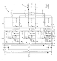
- Fig. 1 shows a current-voltage converter 10 which is connected via a diode D1 to D4 comprehensive rectifier 12 with a mains voltage U network .
- the mains voltage U net in this embodiment is typically in the range of 1000 to 1500 VAC and may have a frequency of 16 2/3 Hz to 400 Hz. Also, input voltages in the range of 1500 VDC to 3000 VDC are possible.
- a sinusoidal pulsating, half-wave input AC voltage U E which is converted by the voltage converter 10 in a constant output voltage U A.
- the current-voltage converter 10 has a primary side 14, which has a plurality of series connected Subsystems 16, 18, 20, each having at least one transistor power switch T1, T2, T3.
- the subsystems 16, 18, 20 are shown in the here Embodiment designed as a SEPIC converter or regenerators whose Output in each case with a primary winding TP1, TP2, TP3 of an isolating transformer TR1, TR2, TR3 is connected.
- the isolation transformers TR1, TR2, TR3 each have secondary coils TS1, TS2, TS3, via a secondary side 22 of the voltage converter 10 are coupled to a common load output 24.
- the subsystem 20 includes a SEPIC converter 26, a primary side Input 28 to which an inductance as input inductor L20.1 connected is connected via a capacitor 30 and a diode 32 to a first terminal 34 of the Transformer primary winding TP3 is connected. Another connection 36 is with a primary-side output 38 of the SEPIC converter 26 connected. Between the input side Throttle L20.1 and the capacitor 30 is a junction 40, the over a ballast network 42 having a first terminal 44 of the transistor power switching element T3 is connected. Another port 46 of the transistor power switch T3 is connected to the output 38.
- a control input 48 of the transistor power switch T3 is via a secondary winding of a transformer 50 with the Output 38 connected. Between the capacitor 30 and the diode 32 is a junction 52, which has a second choke L20.2 and a resistor 56 like shunt connected to the output 38. Parallel to the primary-side transformer winding TP3 is a relief network as a series circuit of capacitor 58 and resistor 60 arranged.
- the secondary winding TS3 of the isolation transformer TR3 is connected to a peak rectification circuit 62 consisting of the diode D5, at whose output a capacitor 64 is located.
- the secondary winding TS2 is also followed by a rectifier circuit 66, at whose output a capacitor 68 is located.
- the same applies to the secondary winding TS1 which is followed by a rectifier circuit 70, at whose output a capacitor 72 is located.
- the secondary side 22 consists essentially of three secondary systems 74, 76, 78, each consisting of the secondary transformer winding, the associated and associated rectifier and the output capacitor.
- the secondary systems 74, 76, 78 are electrically connected in parallel and form an output 80 to which the regulated output voltage U A can be tapped via a filter network 82.
- the capacitors 64, 68, 72 can also be designed as a single common capacitor with a large capacity.
- the windings of the isolation transformers are on a separate transformer core 84, 84 ', 84 "Alternatively, however, there is the possibility of the windings with a corresponding ratio of the voltages and currents on a common Core to arrange.
- each stage is located at one third of the input voltage U E.
- drive windings are the transformers 50, 50', 50 "arranged on a common magnetic core. Alternatively, however, it is possible to design the drive windings as separate transformers, especially at very high input voltages.
- a current flows from the positive pole 86 of the rectifier 12 via an input inductor L16.1 of the subsystem 16, a ballast network 42 "and the transistor power switch T1, as well as via the Input inductor L18.1, Snubbernetzteil 42 'and the transistor power switch T2 and via the input choke L20.1, the ballast power supply 42 and the transistor power switch T3 to the negative pole 88 of the rectifier.
- the capacitors 90, 90 ', 90 " at which in each case only 1/3 of the input voltage U E drops, are located parallel to the inputs of the respective subsystems 16, 18, 20.
- the otherwise usual very large storage capacitor the primary direct access of the input voltage withdrawn and transformed to the low-voltage or secondary side and charged there short-circuit current controlled.
- a current-voltage converter 92 is shown, which is connected via a rectifier 94 to the diodes D6 - D9 with mains voltage U network .
- the line voltage U network is typically in the range of 110 - 234 VAC or 28 - 48 VAC and may have a frequency of 16 2/3 Hz - 400 Hz.
- Mains voltages in the range of 4 - 72 or 14.4 - 154 VDC are also possible.
- the current-voltage converter 92 is designed in particular for high input currents I E and output currents I A.
- the current-voltage converter 92 has a primary side 96, which has a plurality of parallel connected Subsystems 98, 100, 102, each having at least one transistor power switch T4, T6, T7.
- Subsystems 98, 100, 102 are in this illustrated embodiment designed as a SEPIC converter or regenerators, whose output is in each case connected to a primary winding TP4, TP5, TP6 of an isolating transformer TR4, TR5, TR6 is connected.
- the isolating transformers TR4, TR5, TR6 each have Secondary coils TS4, TS5, TS6, which via a secondary side 104 of the voltage-current converter 92 are coupled to a common load output 106.
- the structure of the subsystems 98, 100, 102 substantially corresponds to the subsystems 16, 18, 20, which have been described in detail with reference to FIG.
- the primary-side parallel connection of the regenerators or SEPIC converters 98, 100, 102 with the potential separation reduces the current flowing through a transistor power switch T4, T5, T6 to one third of the input current I E. For this reason, commercially available current-carrying transistors can be used.
- the drive transmitters 108, 110, 112 in the parallel circuit described here are on a common core.
- the drive transmitters 108, 110, 112 may also be embodied as electronic semiconductor power drivers (not shown).
- the subsystems 98, 100, 102 have input-side inductances L 98.1, L 100.1, L 102.1, which are at least temporarily parallel to the input voltage U E via the transistor power switches and thus effect a current balancing of the overall system.
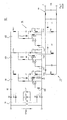
- the regulation of the current-voltage converter is based on the control circuit of FIG. 3rd be explained.
- FIG. 3 shows a control loop arrangement for controlling at least one subsystem 16, 18, 20 or 98, 100, 102 of the current-voltage converter 10 or 92 according to FIG. 1 or 2.
- the control circuit 200 has on the input side a voltage comparator 202, which has a first input 204 with a reference voltage U ARef and a second input 206 via a sampling circuit 208 such as sample and hold circuit or continuous measurement with the output voltage U A for tapping an actual Voltage U Alst is connected.
- the output voltage U A is measured via an unillustrated measuring element at the output 24 of the current-voltage converter or via the load voltage U A 'at the primary transformer winding TP1 - TP6 during the T OFF phase.
- An output 210 of the comparator 202 is connected to an input 212 of an amplifier 214 in order to amplify a differential voltage _U A formed from the actual voltage U Alst and the reference voltage U ARef .
- an output 216 of the amplifier 214 is an error amplified voltage K U x _ U A , which is supplied to an input 218 of a multiplying D / A converter 220.
- Another input 222 of the D / A converter 220 is connected to an output 224 of a circuit, preferably microcontroller 226.
- the microcontroller 226 is in turn connected via a feed line 228 to a power line or to the mains voltage U Netz .
- the microcontroller 226 is connected via an output 230 and a trigger line 232 to an input 234 of the sampling circuit 208.
- a further input 242 of the comparator 240 is connected via a feed line 138 to the shunt 56 in the branch of the choke coil 220.1 for tapping a size I A 'proportional to the output current I A.
- An output 244 of the comparator is connected to an input 246 of a current amplifier 248.
- At an output 250 of the amplifier is applied to an amplified current difference K 1 x _I A , which is supplied to a drive unit 252 and forms a controlled variable.
- the drive unit further has an input 254 for the mains or input voltage for T ON control and an output 256 for driving the transistor power switches TI and T6 via drive transformers 50, 50 ', 50 "and 108 - 112, respectively Size K, x _I A , the T OFF time of the transistor power switches T1-T6 is controlled or regulated, and even without a U / I controller, T ON control and specification of the T OFF voltage as a DC value become a quasi-constant Output voltage with sinusoidal current consumption at AC voltage supply and changing input range or output load achieved.
- the processing After detection and storage of the time base, the processing starts with a trigger zero crossing and synchronize about it at further zero crossings. Synchronization pulses, which lie between the mathematical zero crossings hidden because of possible disturbances.
- the generated sinusoidal waveform is output via the output 224 to the input 226 of the D / A converter 220.
- the sampling circuit 208 is triggered with a synchronization pulse applied to each half-wave zero crossing.
- the error-amplified differential voltage K U x _U A is now multiplied by the synthetic sinusoid Bmax x
- a sine-weighted voltage- fault -amplified variable is present at the output, which is available as a set current I ASoll for driving the transistor power switches T1-T6.
- there is no need for an additional correction element since the size of the output current in the primary-side choke branch is independent of long-term fluctuations of the input voltage U E but follows the nominal frequency waveform (PFC).
- the sine function generated in the microcontroller can also be used as a reference for under- or overvoltage detection.
- the sine function generated in the microcontroller can be determined by means of a comparator circuit be synchronized to the network.
- the microcontroller 226 detects that the input voltage is a DC voltage, so at the output 224 is a constant voltage B so that a PFC rating is eliminated.
- the described system of current-voltage converter 10, 92 and inventive Control circuit 200 comes in particular in the railway area at four UIC voltages, such as for example, 1000 VAC 16 2/2 Hz, 1500 VAC 50 Hz, 1500 VDC and 3000 VDC to Application. Because the voltage converter or regenerator has a wide input voltage range allows, the problem is whether input AC voltage or DC input voltage or which frequency the input AC voltage has, by the previously stated features solved. However, all four ranges as well as tolerances (+ - 30%) and long-term transients in an input voltage range are processed.
- FIG. 4 shows a current-voltage converter 400 with an independent inventive character.
- the current-voltage converter 400 has a primary side 402, which is connected to mains voltage U Netz via a rectifier 404, and a secondary side 406, which has a plurality, ie multiple, preferably three, outputs 408, 410, 412 with the output voltages U A1 , U A2 , U A3 .
- Parallel to output terminals 414, 416 of the rectifier 404 is a capacitor 418 to which an input voltage U E for the current-voltage converter 400 is applied.
- a primary inductor such as choke coil L420.1
- L420.1 Connected to terminal 414 is a primary inductor, such as choke coil L420.1, which is connected via a capacitor 422 and a diode 424 to a first terminal 426 of a primary-side winding TP7 of an isolation transformer TR.
- the primary-side winding TP7 is connected to the input terminal 416 of the rectifier 404.
- Between the inductor L420.1 and the capacitor 422 is a junction 430 which is connected to the terminal 416 via a snubber network 432 and a transistor power switch T7.
- a control terminal 434 of the transistor power switch T7 is connected to the terminal 416 via a secondary winding 436 of a Anberichtübertragers 438.
- a junction 440 located between the capacitor 422 and the diode 424 is also connected to the terminal 416 via a second inductance such as choke coil L 420.2 and a measuring element in series therewith such as shunt 444.
- the secondary-side multiple outputs 408, 410, 412 each have a secondary winding TS7.1, TS7.2, TS7.3, which are arranged together with the primary winding TP7 on a common core 446.
- the secondary windings TS7.1, TS7.2, TS7.3 are each connected via a rectifier diode 448, 450, 452 to an output capacitor 454, 456, 458, to which the output voltage U A1 , U A2 and U A3 are applied.
- the current-voltage converter 400 is characterized by the fact that a feedback of controlled variables or monitoring functions of secondary-side sizes is not required. This is made possible, in particular, by the fact that the output voltage on the primary side during the T Off time at the terminal 426 of the primary winding TP7 and the output current (average size) on the primary side on the measuring element 440 can be measured. The input voltage can be measured on the secondary side during the T On time.
Landscapes
- Engineering & Computer Science (AREA)
- Power Engineering (AREA)
- Dc-Dc Converters (AREA)
- Measuring Instrument Details And Bridges, And Automatic Balancing Devices (AREA)
- Measurement Of Current Or Voltage (AREA)
- Ignition Installations For Internal Combustion Engines (AREA)
- Details Of Television Scanning (AREA)
Abstract
Description
- Fig. 1
- einen kaskadierten Strom-Spannungswandler mit drei primärseitig in Reihe geschalteten Teilsystemen, wobei die Teilsysteme als SEPIC-Wandler ausgebildet sind,
- Fig. 2
- einen Strom-Spannungswandler mit drei primärseitig parallel geschalteten Teilsystemen,
- Fig. 3
- eine Regelkreisanordnung für zumindest ein Teilsystem des Spannungswandlersystems gemäß Fig. 1 oder Fig. 2 und
- Fig. 4
- einen Strom-Spannungswandler mit sekundärseitig multiplen Ausgängen.
Claims (12)
- Strom-Spannungswandler (400) mit einem Eingang (414), an dem eine erste Induktivität (L420.1) angeschlossen ist, die über einen Kondensator (422) und eine Diode (424) mit einer in einem ersten Anschluss (426) einer Primärwicklung (TP7) eines Trenntransformators (TR) verbunden ist, der mit seinem zweiten Anschluss (428) mit einem Ausgang (416) verbunden ist, wobei eine Verbindungsstelle (430) zwischen der ersten Induktivität (L420.1) und dem Kondensator (422) über ein Leistungs-Schaltelement (T7) mit dem Ausgang (416) verbunden ist und wobei eine Verbindungsstelle (440) zwischen dem Kondensator (422) und der Diode (424) über eine Reihenschaltung aus zweiter Induktivität (420.2) und Messelement (444) mit dem Ausgang (416) verbunden ist,
dadurch gekennzeichnet, dass der Trenntransformator (TR) mehrere auf einem gemeinsamen Kern (446) angeordnete Sekundärwicklungen (TS7.1, TS7.2, TS7.3) zur Bildung multipler Ausgänge aufweist. - Strom-Spannungswandler nach Anspruch 1,
dadurch gekennzeichnet, dass der Strom-Spannungswandler (400) im nicht stromlückenden Betrieb arbeitet. - Strom-Spannungswandler nach Anspruch 1,
dadurch gekennzeichnet, dass eine den Ausgangsspannungen UA1, UA2, UA3 proportionale Größe UA' an der primären Trafowicklung (TP7) abgreifbar ist. - Strom-Spannungswandler nach Anspruch 1,
dadurch gekennzeichnet, dass eine den Ausgangsströmen IA1, IA2, IA3 proportionale Größe IA' an dem in Reihe zu der zweiten Induktivität (L420.2) liegenden Messelement (444) wie Shunt messbar ist. - Strom-Spannungswandler nach Anspruch 1,
dadurch gekennzeichnet, dass die Sekundärwicklungen (TS7.1, TS7.2, TS7.3) zur Einstellung der verschiedenen Ausgangsspannung UA1, UA2, UA3 unterschiedliche Windungszahlen aufweisen. - Strom-Spannungswandler nach Anspruch 1,
dadurch gekennzeichnet, dass die Ausgangsspannungen UA1, UA2, UA3 konstant sind. - Strom-Spannungswandler nach Anspruch 1,
dadurch gekennzeichnet, dass eine Zusatzwicklung oder eine Sekundärwicklung und/oder die Primärwicklung selbst als Messwicklung ausgebildet sind und Regelgrößen für einen Regelkreis zur Verfügung stellt. - Regelkreis (200) für einen Strom-Spannungswandler (400) nach einem der Ansprüche 1 bis 7, umfassend einen Spannungsregler mit Spannungsvergleicher und Spannungsverstärker sowie einen Stromregler mit Stromvergleicher und Stromverstärker sowie ein zwischen Spannungsregler und Stromregler angeordnetes Korrekturglied,
dadurch gekennzeichnet, dass der Regelkreis einen Schaltkreis (226) zur Erfassung der Netzspannung und/oder Netzfrequenz aufweist, dass der Schaltkreis (226) mit einer Abtastschaltung (208) verbunden ist, die mit einem Eingang an einer der Ausgangsspannung UA proportionalen Größe UA' liegt und mit einem Ausgang mit dem Spannungsvergleicher (202) verbunden ist und dass der Spannungsregler ausgangsseitig mit einem ersten Eingang (218) eines D/A-Wandlers (220) verbunden ist, der seinerseits mit einem zweiten Eingang (222) mit einem Ausgang (224) des Schaltkreises (226) und ausgangsseitig mit einem Eingang (238) des Stromvergleichers (240) des Stromreglers verbunden ist. - Regelkreis nach Anspruch 8,
dadurch gekennzeichnet, dass der Schaltkreis (226) eine Schaltung zur Erfassung der Netzspannung und/oder Netzfrequenz, eine Schaltung zur Erzeugung einer synthetischen Sinusfunktion, eine Triggerschaltung sowie eine Synchronisationsschaltung aufweist. - Regelkreis nach Anspruch 8,
dadurch gekennzeichnet, dass am Ausgang (224) des Schaltkreises (226) ein synthetischer Sinus B = Bmax |sin (ωt)| mit konstanter Amplitude B zur Verfügung steht, der die tatsächliche Netzfrequenz repräsentiert. - Regelkreis nach einem der zuvor genannten Ansprüche,
dadurch gekennzeichnet, dass am Ausgang (230) des Schaltkreises (226) ein Triggersignal für die AbtastSchaltung (208) zur Verfügung steht. - Regelkreis nach einem der zuvor genannten Ansprüche,
dadurch gekennzeichnet, dass in dem Schaltkreis (226) vorprogrammierte Sinusfunktionen abgelegt sind.
Applications Claiming Priority (3)
| Application Number | Priority Date | Filing Date | Title |
|---|---|---|---|
| DE19800105 | 1998-01-05 | ||
| DE19800105A DE19800105A1 (de) | 1998-01-05 | 1998-01-05 | Strom-Spannungswandler und zugehöriger Regelkreis |
| EP99100017A EP0928059B1 (de) | 1998-01-05 | 1999-01-04 | Strom-Spannungswandler und zugehöriger Regelkreis |
Related Parent Applications (2)
| Application Number | Title | Priority Date | Filing Date |
|---|---|---|---|
| EP99100017A Division EP0928059B1 (de) | 1998-01-05 | 1999-01-04 | Strom-Spannungswandler und zugehöriger Regelkreis |
| EP99100017.5 Division | 1999-01-04 |
Publications (2)
| Publication Number | Publication Date |
|---|---|
| EP1589647A2 true EP1589647A2 (de) | 2005-10-26 |
| EP1589647A3 EP1589647A3 (de) | 2013-04-24 |
Family
ID=7853979
Family Applications (2)
| Application Number | Title | Priority Date | Filing Date |
|---|---|---|---|
| EP05011676.3A Withdrawn EP1589647A3 (de) | 1998-01-05 | 1999-01-04 | Strom-Spannungsregler und zugehöriger Regelkreis |
| EP99100017A Expired - Lifetime EP0928059B1 (de) | 1998-01-05 | 1999-01-04 | Strom-Spannungswandler und zugehöriger Regelkreis |
Family Applications After (1)
| Application Number | Title | Priority Date | Filing Date |
|---|---|---|---|
| EP99100017A Expired - Lifetime EP0928059B1 (de) | 1998-01-05 | 1999-01-04 | Strom-Spannungswandler und zugehöriger Regelkreis |
Country Status (4)
| Country | Link |
|---|---|
| US (2) | US6094366A (de) |
| EP (2) | EP1589647A3 (de) |
| AT (1) | ATE373334T1 (de) |
| DE (2) | DE19800105A1 (de) |
Families Citing this family (22)
| Publication number | Priority date | Publication date | Assignee | Title |
|---|---|---|---|---|
| WO2001071775A2 (en) | 2000-03-17 | 2001-09-27 | Satcon Technology Corporation | A low-inductance capacitor and a method for minimizing inductance in a snubber circuit |
| DE20018560U1 (de) * | 2000-10-30 | 2002-03-21 | CAMERON GmbH, 29227 Celle | Steuer- und Versorgungssystem |
| US7615893B2 (en) * | 2000-05-11 | 2009-11-10 | Cameron International Corporation | Electric control and supply system |
| DE20115474U1 (de) | 2001-09-19 | 2003-02-20 | Biester, Klaus, 29342 Wienhausen | Gleichspannungs-Wandlervorrichtung |
| DE20115473U1 (de) * | 2001-09-19 | 2003-02-20 | Biester, Klaus, 29342 Wienhausen | Universelles Energieversorgungssystem |
| DE20115471U1 (de) * | 2001-09-19 | 2003-02-20 | Biester, Klaus, 29342 Wienhausen | Universelles Energieversorgungssystem |
| DE10100862A1 (de) * | 2001-01-11 | 2002-07-18 | Philips Corp Intellectual Pty | Konvertersystem und Netzteil zum Umsetzen einer Eingangsgleichspannung in eine Ausgangsgleichspannung |
| US7020271B2 (en) * | 2003-06-12 | 2006-03-28 | Barbara Isabel Hummel | Ring control device |
| DE20115475U1 (de) * | 2001-09-19 | 2003-02-20 | Biester, Klaus, 29342 Wienhausen | Gleichspannungs-Wandlervorrichtung |
| US20050135034A1 (en) * | 2003-12-19 | 2005-06-23 | Caterpillar, Inc. | Resettable circuit breaker |
| ES2365917T3 (es) * | 2004-02-12 | 2011-10-13 | Mitsubishi Denki Kabushiki Kaisha | Convertidor de potencia. |
| DE102004020792B4 (de) * | 2004-04-28 | 2013-06-06 | Leopold Kostal Gmbh & Co. Kg | Elektrischer Schaltwandler mit hoher Eingangsspannung |
| DE102004043609A1 (de) | 2004-09-07 | 2006-03-30 | Reinhard Kalfhaus | Spannungswandler |
| CN102013826A (zh) * | 2010-12-01 | 2011-04-13 | 北京理工大学 | 输入串联输出并联型高频链逆变器模块的稳定电流控制方法 |
| WO2014120153A1 (en) * | 2013-01-30 | 2014-08-07 | Schneider Electric It Corporation | Flyback converter |
| US20140268927A1 (en) | 2013-03-14 | 2014-09-18 | Vanner, Inc. | Voltage converter systems |
| JP6357976B2 (ja) * | 2014-08-26 | 2018-07-18 | 富士電機株式会社 | 直流電源装置 |
| US10135344B2 (en) | 2016-07-13 | 2018-11-20 | Silanna Asia Pte Ltd | Lossless snubber circuits |
| WO2018125104A1 (en) * | 2016-12-28 | 2018-07-05 | Halliburton Energy Services, Inc. | Current-to-voltage power converter |
| DE102019202211A1 (de) * | 2019-02-19 | 2020-08-20 | Richter R & W - Steuerungstechnik GmbH | Vorrichtung zur Symmetrisierung einer Stromabnahme von Außenleitern eines mehrphasigen Niederspannungsnetzes |
| CN112701920B (zh) * | 2020-12-21 | 2023-02-10 | 成都芯源系统有限公司 | 一种多路输出电路的控制电路及其反馈电路 |
| US20260018920A1 (en) * | 2024-07-12 | 2026-01-15 | GM Global Technology Operations LLC | Power conversion system for a vehicle |
Citations (5)
| Publication number | Priority date | Publication date | Assignee | Title |
|---|---|---|---|---|
| US4974141A (en) | 1988-05-18 | 1990-11-27 | Viteq Corporation | AC to DC power converter with input current waveform control for buck-boost regualtion of output |
| US5006975A (en) | 1989-11-03 | 1991-04-09 | Cherry Semiconductor Corporation | Power factor correction circuit |
| DE4414677A1 (de) | 1994-04-27 | 1995-11-02 | Pintsch Bamag Ag | Primärgetakteter Spannungswandler, insbesondere für hohe Eingangsgleichspannungen |
| DE19515210A1 (de) | 1995-04-28 | 1996-10-31 | Reinhard Kalfhaus | Schaltnetzteil, insbesondere Netzregenerator |
| DE19609123A1 (de) | 1996-03-08 | 1997-09-18 | Siemens Ag | Schaltungsanordnung für Schaltnetzteile mit mehreren lastunabhängigen Ausgangsspannungen |
Family Cites Families (12)
| Publication number | Priority date | Publication date | Assignee | Title |
|---|---|---|---|---|
| FR2063511A5 (de) * | 1969-10-20 | 1971-07-09 | Sautel Auguste | |
| US4062057A (en) * | 1977-04-15 | 1977-12-06 | The United States Of America As Represented By The Secretary Of The Navy | Regulated power supply having a series arrangement of inverters |
| GB1554835A (en) * | 1978-02-01 | 1979-10-31 | Marconi Co Ltd | Inverter circuits |
| JPS5967869A (ja) * | 1982-10-08 | 1984-04-17 | Fuji Electric Co Ltd | Dc−dcコンバ−タ装置 |
| DE3242023A1 (de) * | 1982-11-12 | 1984-05-17 | Siemens AG, 1000 Berlin und 8000 München | Schaltungsanordnung zur speisung von elektrischen verbrauchern mit einer gleichspannung |
| GB2152770B (en) * | 1983-11-15 | 1987-04-29 | Yokogawa Hokushin Electric | Dc/dc converter |
| US4581692A (en) * | 1984-10-04 | 1986-04-08 | Westinghouse Electric Corp. | Direct current voltage converter apparatus |
| US5146396A (en) * | 1991-06-17 | 1992-09-08 | At&T Bell Laboratories | Single stage power factor corrected converter having isolated output |
| DE9403447U1 (de) * | 1994-03-01 | 1994-04-28 | Siemens AG, 80333 München | Energieversorgungseinrichtung für Reisezugwagen |
| US5602465A (en) * | 1994-08-30 | 1997-02-11 | International Rectifier Corporation | Method and circuit to improve output voltage regulation and noise rejection of a power factor control stage |
| DE19505417C2 (de) * | 1995-02-17 | 2001-03-08 | Reinhard Kalfhaus | SEPIC-Schaltnetzteil |
| US5804890A (en) * | 1995-07-07 | 1998-09-08 | Lucent Technologies Inc. | Direct current voltage power backup system |
-
1998
- 1998-01-05 DE DE19800105A patent/DE19800105A1/de not_active Withdrawn
-
1999
- 1999-01-04 EP EP05011676.3A patent/EP1589647A3/de not_active Withdrawn
- 1999-01-04 US US09/224,835 patent/US6094366A/en not_active Expired - Lifetime
- 1999-01-04 DE DE59914492T patent/DE59914492D1/de not_active Expired - Lifetime
- 1999-01-04 AT AT99100017T patent/ATE373334T1/de active
- 1999-01-04 EP EP99100017A patent/EP0928059B1/de not_active Expired - Lifetime
-
2000
- 2000-05-30 US US09/580,956 patent/US6181586B1/en not_active Expired - Lifetime
Patent Citations (5)
| Publication number | Priority date | Publication date | Assignee | Title |
|---|---|---|---|---|
| US4974141A (en) | 1988-05-18 | 1990-11-27 | Viteq Corporation | AC to DC power converter with input current waveform control for buck-boost regualtion of output |
| US5006975A (en) | 1989-11-03 | 1991-04-09 | Cherry Semiconductor Corporation | Power factor correction circuit |
| DE4414677A1 (de) | 1994-04-27 | 1995-11-02 | Pintsch Bamag Ag | Primärgetakteter Spannungswandler, insbesondere für hohe Eingangsgleichspannungen |
| DE19515210A1 (de) | 1995-04-28 | 1996-10-31 | Reinhard Kalfhaus | Schaltnetzteil, insbesondere Netzregenerator |
| DE19609123A1 (de) | 1996-03-08 | 1997-09-18 | Siemens Ag | Schaltungsanordnung für Schaltnetzteile mit mehreren lastunabhängigen Ausgangsspannungen |
Also Published As
| Publication number | Publication date |
|---|---|
| EP0928059B1 (de) | 2007-09-12 |
| EP1589647A3 (de) | 2013-04-24 |
| DE19800105A1 (de) | 1999-07-15 |
| DE59914492D1 (de) | 2007-10-25 |
| EP0928059A3 (de) | 2002-03-13 |
| US6181586B1 (en) | 2001-01-30 |
| EP0928059A2 (de) | 1999-07-07 |
| US6094366A (en) | 2000-07-25 |
| ATE373334T1 (de) | 2007-09-15 |
Similar Documents
| Publication | Publication Date | Title |
|---|---|---|
| EP1589647A2 (de) | Strom-Spannungsregler und zugehöriger Regelkreis | |
| DE69712243T2 (de) | Universeller Leistungsmodul | |
| EP1497910B1 (de) | Schaltnetzteilanordnung | |
| DE102018112088A1 (de) | Pwm-gesteuerter resonanzwandler | |
| DE3441631A1 (de) | Umrichter | |
| DE102016115432A1 (de) | System und Verfahren zur Spannungseinstellung für Parallelstufen-Leistungswandler | |
| DE3537175A1 (de) | Gleichspannungswandler | |
| DE10122534A1 (de) | Resonanter Konverter | |
| DE102014105289A1 (de) | Aktiver EMV Filter | |
| DE3111088A1 (de) | Magnetverstaerker und schaltnetzteil | |
| DE10020357A1 (de) | DC-DC-Konverter | |
| EP0951133A2 (de) | Verfahren und aktives Filter zur Reduzierung der Restwelligkeit des einem Netz durch eine Last entnommenen Stroms | |
| DE60113166T2 (de) | Geregelter Resonanzwandler | |
| EP0772902B1 (de) | Stromversorgungsgerät, insbesondere batterie-ladegerät für elektrofahrzeuge oder dergleichen | |
| DE2825240C2 (de) | Rundsteueranlage | |
| EP0162374B1 (de) | Schaltungsanordnung für Umrichter | |
| DE3040556C2 (de) | ||
| DE10133865A1 (de) | Elektrische Schaltungsanordnung | |
| EP1670129B1 (de) | Spannungswandler | |
| DE69415940T2 (de) | Wechselstrom-Gleichstromwandler mit einer Filtervorrichtung | |
| DE4038869C1 (en) | Current symmetrising circuitry for parallel converters - having branches of semiconductor switches and phase outputs coupled together via choke coils | |
| EP4173125A1 (de) | Dreiphasen boost-converter mit pfc | |
| DE69735789T2 (de) | Geregelter Resonanzwandler | |
| CH712011A2 (de) | Konverter zur potentialgetrennten Übertragung elektrischer Energie. | |
| EP0066904A1 (de) | Schaltverstärker |
Legal Events
| Date | Code | Title | Description |
|---|---|---|---|
| PUAI | Public reference made under article 153(3) epc to a published international application that has entered the european phase |
Free format text: ORIGINAL CODE: 0009012 |
|
| AC | Divisional application: reference to earlier application |
Ref document number: 0928059 Country of ref document: EP Kind code of ref document: P |
|
| AK | Designated contracting states |
Kind code of ref document: A2 Designated state(s): AT CH DE DK FR GB LI SE |
|
| PUAL | Search report despatched |
Free format text: ORIGINAL CODE: 0009013 |
|
| AK | Designated contracting states |
Kind code of ref document: A3 Designated state(s): AT CH DE DK FR GB LI SE |
|
| RIC1 | Information provided on ipc code assigned before grant |
Ipc: H02M 3/28 20060101AFI20130318BHEP Ipc: H02M 3/335 20060101ALI20130318BHEP Ipc: H02M 1/00 20070101ALI20130318BHEP |
|
| 17P | Request for examination filed |
Effective date: 20131018 |
|
| RBV | Designated contracting states (corrected) |
Designated state(s): AT CH DE DK FR GB LI SE |
|
| GRAP | Despatch of communication of intention to grant a patent |
Free format text: ORIGINAL CODE: EPIDOSNIGR1 |
|
| AKX | Designation fees paid |
Designated state(s): AT CH DE DK FR GB LI SE |
|
| INTG | Intention to grant announced |
Effective date: 20131217 |
|
| STAA | Information on the status of an ep patent application or granted ep patent |
Free format text: STATUS: THE APPLICATION IS DEEMED TO BE WITHDRAWN |
|
| 18D | Application deemed to be withdrawn |
Effective date: 20140429 |