EP1589369A2 - Spiegel mit variablem Reflektionsgrad - Google Patents
Spiegel mit variablem Reflektionsgrad Download PDFInfo
- Publication number
- EP1589369A2 EP1589369A2 EP05008906A EP05008906A EP1589369A2 EP 1589369 A2 EP1589369 A2 EP 1589369A2 EP 05008906 A EP05008906 A EP 05008906A EP 05008906 A EP05008906 A EP 05008906A EP 1589369 A2 EP1589369 A2 EP 1589369A2
- Authority
- EP
- European Patent Office
- Prior art keywords
- layer
- color
- color layer
- variable reflectance
- hydrogen
- Prior art date
- Legal status (The legal status is an assumption and is not a legal conclusion. Google has not performed a legal analysis and makes no representation as to the accuracy of the status listed.)
- Withdrawn
Links
Images


Classifications
-
- G—PHYSICS
- G02—OPTICS
- G02F—OPTICAL DEVICES OR ARRANGEMENTS FOR THE CONTROL OF LIGHT BY MODIFICATION OF THE OPTICAL PROPERTIES OF THE MEDIA OF THE ELEMENTS INVOLVED THEREIN; NON-LINEAR OPTICS; FREQUENCY-CHANGING OF LIGHT; OPTICAL LOGIC ELEMENTS; OPTICAL ANALOGUE/DIGITAL CONVERTERS
- G02F1/00—Devices or arrangements for the control of the intensity, colour, phase, polarisation or direction of light arriving from an independent light source, e.g. switching, gating or modulating; Non-linear optics
- G02F1/01—Devices or arrangements for the control of the intensity, colour, phase, polarisation or direction of light arriving from an independent light source, e.g. switching, gating or modulating; Non-linear optics for the control of the intensity, phase, polarisation or colour
- G02F1/15—Devices or arrangements for the control of the intensity, colour, phase, polarisation or direction of light arriving from an independent light source, e.g. switching, gating or modulating; Non-linear optics for the control of the intensity, phase, polarisation or colour based on an electrochromic effect
- G02F1/153—Constructional details
- G02F1/157—Structural association of cells with optical devices, e.g. reflectors or illuminating devices
-
- B—PERFORMING OPERATIONS; TRANSPORTING
- B82—NANOTECHNOLOGY
- B82Y—SPECIFIC USES OR APPLICATIONS OF NANOSTRUCTURES; MEASUREMENT OR ANALYSIS OF NANOSTRUCTURES; MANUFACTURE OR TREATMENT OF NANOSTRUCTURES
- B82Y20/00—Nanooptics, e.g. quantum optics or photonic crystals
-
- G—PHYSICS
- G02—OPTICS
- G02F—OPTICAL DEVICES OR ARRANGEMENTS FOR THE CONTROL OF LIGHT BY MODIFICATION OF THE OPTICAL PROPERTIES OF THE MEDIA OF THE ELEMENTS INVOLVED THEREIN; NON-LINEAR OPTICS; FREQUENCY-CHANGING OF LIGHT; OPTICAL LOGIC ELEMENTS; OPTICAL ANALOGUE/DIGITAL CONVERTERS
- G02F1/00—Devices or arrangements for the control of the intensity, colour, phase, polarisation or direction of light arriving from an independent light source, e.g. switching, gating or modulating; Non-linear optics
- G02F1/01—Devices or arrangements for the control of the intensity, colour, phase, polarisation or direction of light arriving from an independent light source, e.g. switching, gating or modulating; Non-linear optics for the control of the intensity, phase, polarisation or colour
- G02F1/15—Devices or arrangements for the control of the intensity, colour, phase, polarisation or direction of light arriving from an independent light source, e.g. switching, gating or modulating; Non-linear optics for the control of the intensity, phase, polarisation or colour based on an electrochromic effect
- G02F1/153—Constructional details
- G02F1/155—Electrodes
-
- G—PHYSICS
- G02—OPTICS
- G02F—OPTICAL DEVICES OR ARRANGEMENTS FOR THE CONTROL OF LIGHT BY MODIFICATION OF THE OPTICAL PROPERTIES OF THE MEDIA OF THE ELEMENTS INVOLVED THEREIN; NON-LINEAR OPTICS; FREQUENCY-CHANGING OF LIGHT; OPTICAL LOGIC ELEMENTS; OPTICAL ANALOGUE/DIGITAL CONVERTERS
- G02F1/00—Devices or arrangements for the control of the intensity, colour, phase, polarisation or direction of light arriving from an independent light source, e.g. switching, gating or modulating; Non-linear optics
- G02F1/01—Devices or arrangements for the control of the intensity, colour, phase, polarisation or direction of light arriving from an independent light source, e.g. switching, gating or modulating; Non-linear optics for the control of the intensity, phase, polarisation or colour
- G02F1/15—Devices or arrangements for the control of the intensity, colour, phase, polarisation or direction of light arriving from an independent light source, e.g. switching, gating or modulating; Non-linear optics for the control of the intensity, phase, polarisation or colour based on an electrochromic effect
- G02F1/153—Constructional details
- G02F1/1533—Constructional details structural features not otherwise provided for
- G02F2001/1536—Constructional details structural features not otherwise provided for additional, e.g. protective, layer inside the cell
-
- G—PHYSICS
- G02—OPTICS
- G02F—OPTICAL DEVICES OR ARRANGEMENTS FOR THE CONTROL OF LIGHT BY MODIFICATION OF THE OPTICAL PROPERTIES OF THE MEDIA OF THE ELEMENTS INVOLVED THEREIN; NON-LINEAR OPTICS; FREQUENCY-CHANGING OF LIGHT; OPTICAL LOGIC ELEMENTS; OPTICAL ANALOGUE/DIGITAL CONVERTERS
- G02F2202/00—Materials and properties
- G02F2202/36—Micro- or nanomaterials
-
- G—PHYSICS
- G02—OPTICS
- G02F—OPTICAL DEVICES OR ARRANGEMENTS FOR THE CONTROL OF LIGHT BY MODIFICATION OF THE OPTICAL PROPERTIES OF THE MEDIA OF THE ELEMENTS INVOLVED THEREIN; NON-LINEAR OPTICS; FREQUENCY-CHANGING OF LIGHT; OPTICAL LOGIC ELEMENTS; OPTICAL ANALOGUE/DIGITAL CONVERTERS
- G02F2203/00—Function characteristic
- G02F2203/02—Function characteristic reflective
Definitions
- the present invention relates to a variable reflectance mirror that changes its reflectance by developing and fading color of a color layer provided on the side of a light-reflecting layer thereof electrically, or by hydrogencontaining gas or the like.
- Variable reflectance mirrors that change their reflectance by electrically coloring color layers formed on surfaces of light-reflecting layers, has been conventionally known (e.g., Japanese Utility Model Application Publication (JP-Y) No. 62-2587).
- JP-Y Japanese Utility Model Application Publication
- variable reflectance mirror In the variable reflectance mirror disclosed in JP-Y No. 62-2587, thin layers consisting of a transparent electrode, hydroxide iridium (Ir(OH) 3 ) layer, tantalum pentoxide (Ta 2 O 5 ) layer, tungsten trioxide (WO 3 ) layer, and an aluminum (Al) electrode, are formed (laminated) in this order on a rear surface of a glass substrate by means of, for example, a vacuum deposition.
- the variable reflectance mirror when a voltage is applied between the transparent electrode and the aluminum electrode, the iridium hydroxide layer and the tungsten trioxide layer undergo a coloring reaction, thereby resulting in change of a reflectance of the mirror.
- variable reflectance mirror having the above-described configuration once colored can not be restored to the decolored condition, if thickness and qualities of respective thin layers described above are not well balanced. Further, because fluctuation in thickness of the layers significantly affects properties of the mirror, such mirrors require difficult manufacturing conditions and thus increase in production cost due to use of vacuum deposition or the like for production of the multilayer films.
- variable reflectance mirror with a simpler configuration having only two layers on a rear surface of a glass substrate has been proposed.
- variable reflectance mirror 100 As shown in Figure 6, in the variable reflectance mirror 100, a tungsten trioxide color layer 104 that develops color by binding to hydrogen or lithium is formed on a rear surface of a glass substrate 102, and a light-reflecting rhodium layer 106 that allows permeation of hydrogen or lithium is formed on a side of the color layer 104 that is opposite to side on which the glass substrate 102 is formed.
- the variable reflectance mirror 100 has a supplying device (not shown) that supplies hydrogen or lithium to the color layer 104.
- variable reflectance mirror 100 when hydrogen or lithium is supplied to the color layer 104 by the supplying device, the color layer 104 develops color by binding to hydrogen or lithium. As a result, the light that enters from the surface of the glass substrate 102 (top surface in Figure 6) into the glass substrate 102 and is reflected by the light-reflecting layer 106 becomes reduced in intensity while passing through the colored color layer 104, resulting in decrease in reflectance.
- variable reflectance mirror 100 having the configuration above should have theoretically a high reflectance of 63% when the color layer 104 has been decolored, if the color layer 104 is made of tungsten trioxide and the light-reflecting layer 106 of rhodium as described above.
- the surface 108 becomes uneven and part of the rhodium light-reflecting layer 106 becomes overlapping with the color layer in the irregularities as shown in Figure 6. It has been theoretically confirmed that the presence of such irregularities at the interface between the two layers makes the interface indistinct and thus reduces the reflectance of the mirror when the color layer 104 has been decolored. In addition, an increase in the depth (h) of interface irregularities leads to drastic decrease in reflectance.
- the depth h of the irregularities becomes 10 to 20 nm; and in such a case, it has been confirmed that the reflectance decreases by tens of % to 50% or less as shown in Figure 7.
- the present invention which was made in consideration of the circumstances above, provides a variable reflectance mirror allowing prevention of or control of the deterioration in the reflectance when the color layer has been decolored.
- the invention provides a variable reflectance mirror having: a color layer that can develop color by binding with hydrogen or lithium; a transparent substrate formed on or above one surface of the color layer; a light-reflecting layer formed on the side of the color layer opposite to the surface thereof on which the transparent substrate is formed, which allows transmission of hydrogen or lithium; and a supplying device for supplying hydrogen or lithium to the color layer, wherein a transparent intermediate layer, which allows transmission of hydrogen or lithium and having a refractive index smaller than that of the color layer, is formed between the color layer and the light-reflecting layer.
- variable reflectance mirror when hydrogen or lithium is supplied to the color layer by the supplying device, the color layer develops color by binding to the hydrogen or lithium. As a result, the light that enters from the surface of the transparent substrate into the transparent substrate and is reflected by the light-reflecting layer is reduced in intensity while passing through the colored color layer, altering the reflectance of the variable reflectance mirror and making it exert an anti-glare effect.
- variable reflectance mirror a transparent intermediate layer having a refractive index smaller than that of the color layer is formed between the color layer and the light-reflecting layer. Accordingly, even when there are irregularities on the surface of the color layer facing the light-reflecting layer (at the interface between the color layer and the intermediate layer) and/or on the surface of light-reflecting layer facing the color layer (at the interface between the intermediate layer and light-reflecting layer), the boundary between the color layer and the light-reflecting layer becomes distinct, allowing prevention or control of the deterioration in the reflectance when the color layer has been decolored.
- the invention provides the variable reflectance mirror, in that the material used for the intermediate layer is selected from the group consisting of silicon dioxide, magnesium fluoride, lithium fluoride, and calcium fluoride.
- the material used for the intermediate layer is favorably selected from the group consisting of silicon dioxide, magnesium fluoride, lithium fluoride, and calcium fluoride.
- the invention provides the variable reflectance mirror, in that the thickness of the intermediate layer is 100 nm or less.
- the thickness of the intermediate layer is the minimum distance between the color layer and the light-reflecting layer (the distance in the thickness direction of the transparent substrate between the summit of the irregularities of color layer surface and the summit of the irregularities of the surface of the light-reflecting layer).
- the thickness of the intermediate layer of the variable reflectance mirror is defined as 100 nm or less.
- variable reflectance mirror according to the invention allows prevention or control of the deterioration in the reflectance when the color layer has been decolored.
- variable reflectance mirror according to the present invention will be described in detail.
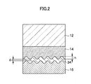
- Figure 1 is a cross-sectional view illustrating the overall configuration of a variable reflectance mirror 10 according to the first embodiment of the invention.
- the variable reflectance mirror 10 has a glass substrate 12 as its transparent substrate.
- a color layer 14 that develops color by binding to hydrogen or lithium is formed as a thin layer on the rear surface of the glass substrate 12 (bottom surface in Figure 1), for example, by means of vacuum deposition.
- the material used for the color layer 14 is tungsten trioxide (WO 3 ).
- a light-reflecting layer 16 that permits transmission of hydrogen or lithium is formed as a thin layer on the surface of the color layer 14 that is opposite to the surface on which the glass substrate 12 is formed, by means of, for example, vacuum deposition.
- the material used for the light-reflecting layer 16 is rhodium.
- a thin layer electrode layer 20 is formed on the surface of the glass substrate 18 (surface facing the glass substrate 12) as a supplying device, for example, by means of vacuum deposition.
- the material used for the electrode layer 20 is chromium or the like.
- the electrolytic solution 24 has a propylene carbonate as the solvent and contains sulfuric acid (H 2 SO 4 ) as a hydrogen ion source, and a neutral material, ferrocene [Fe(C 5 H 5 ) 2 ] as a oxidizing agent.
- a power supply unit 26 is connected to the light-reflecting layer 16 of glass substrate 12 and to the electrode layer 20 of glass substrate 18 via wiring 28.
- the power supply unit 26 has a direct current power supply 30 and a switch 32; and when the switch 32 is turned “ON", the minus electrode of the direct current power supply 30 is connected to the light-reflecting layer 16 and the plus electrode of direct current power supply 30 to the electrode layer 20.
- the light-reflecting layer 16 and the electrode layer 20 may be short-circuited via a circuit (not shown).
- a transparent intermediate layer 34 permitting transmission of hydrogen or lithium and having a refractive index smaller than that of the color layer 14 is formed as a thin layer between the color layer 14 and the light-reflecting layer 16, by means of, for example vacuum deposition.
- the material used for the intermediate layer 34 is lithium fluoride.
- the refractive index of the lithium fluoride intermediate layer 34 is 1.4; and because the refractive index of the tungsten trioxide color layer 14 is approximately 2, the refractive index of the intermediate layer 34 is sufficiently smaller than the refractive index of color layer 14.
- the thickness of the color layer 14 is typically about 500 nm, and the depth h of the irregularities of the surface thereof (surface opposite to the glass substrate 12) is typically about 10 nm.
- the thickness of the light-reflecting layer 16 is typically about 50 nm, and the thickness d of the intermediate layer 34 is typically about 10 nm.
- the thickness "d" of the intermediate layer 34 is a distance in the thickness direction of the glass substrate 12 between the summit of the irregularities of color layer 14 surface (the lowest edge of the irregularities in Figure 2) and the summit of the irregularities of light-reflecting layer 16 surface (the highest edge of the irregularities in Figure 2). Accordingly, for example the thickness d of intermediate layer 34 may be set to 0 or less, as shown in Figure 3.
- variable reflectance mirror 10 having the configuration above, when the switch 32 of the power supply unit 26 is turned "ON", a negative voltage is applied to the light-reflecting layer 16 and a positive voltage to the electrode layer 20 by the direct current power supply 30.
- the hydrogen ions contained in the electrolytic solution 24 are converted to hydrogen atoms at the light-reflecting layer 16, which diffuse though the light-reflecting layer 16 to the color layer 14.
- the following reductive reaction occurs in the color layer 14.
- H + represents a hydrogen ion
- x represents a number in a range of 0 to 0.3
- e - represents an electron.
- the reaction can be represented overall by the following equation.
- Tungsten trioxide (WO 3 ) that is a material for the color layer 14, develops color in accordance with the reaction of the above equation.
- the light that enters from the surface of the glass substrate 12 into the glass substrate 12 and is reflected by the light-reflecting layer 16 (see arrow A in Figure 1) is reduced in intensity by passing through the colored color layer 14, altering the reflectance of the variable reflectance mirror 10 and making it exert an anti-glare effect.
- the switch 32 of the power supply unit 26 is turned "OFF", i.e., when the voltage applied to the light-reflecting layer 16 and the electrode layer 20 is removed and the light-reflecting layer 16 and the electrode layer 20 are short-circuited via a circuit (not shown), the hydrogen atoms diffused into the color layer 14 are converted to hydrogen ions in the light-reflecting layer 16 and conveyed back to the electrolytic solution 24, making the tungsten trioxide (WO 3 ) material of the color layer 14 decolor.
- WO 3 tungsten trioxide
- a lithium fluoride intermediate layer 34 having a refractive index significantly smaller than that of the color layer 14 is formed between the tungsten trioxide color layer 14 and the rhodium light-reflecting layer 16. Presence of the layer, which makes the color layer 14 and the light-reflecting layer 16 boundary distinct, allows prevention or control of the deterioration in reflectance when the color layer 14 has been decolored.
- Figure 4 is a chart showing the theoretical relationship between the thickness d of intermediate layer 34 and the reflectance when the color layer 14 has been decolored in the variable reflectance mirror 10 according to the first embodiment, when the thickness of the tungsten trioxide color layer 14 is set to about 500 nm, the depth h of the irregularities of the color layer 14 surface is set to 10 nm, and the thickness of the rhodium light-reflecting layer 16 is set to 50 nm.
- variable reflectance mirror 10 As is apparent from Figure 4, in the variable reflectance mirror 10 according to the first embodiment having a lithium fluoride intermediate layer 34 having a thickness d of about 10 nm, the reflectance exceeds approximately 60% when the color layer 14 has been decolored, indicating that advantageous effects of the intermediate layer 34 are sufficiently exerted.
- Figure 4 demonstrates that the reflectance when the color layer 14 has been decolored is increased to approximately 64% when, for example, the thickness d of the intermediate layer 34 becomes approximately 20 nm and it is possible to improve the reflectance when the color layer 14 has been decolored by increasing the thickness d of intermediate layer 34.
- an excessively large thickness d of the intermediate layer 34 may result in generation of interference colors; and thus the thickness d of intermediate layer 34 is preferably set to about 100 nm or less.
- variable reflectance mirror 10 allows prevention or control of the deterioration in reflectance when the color layer 14 has been decolored.
- the electrolytic solution 24 for the explanation of the first embodiment contains hydrogen ions
- the electrolyte contained in the electrolytic solution 24 is not limited to hydrogen atoms and may be a configuration with lithium ions.
- Figure 5 is a cross-sectional view illustrating the overall configuration of a variable reflectance mirror 50 according to the second embodiment.
- variable reflectance mirror 50 has a configuration that is basically the same as the variable reflectance mirror 10 according to the first embodiment, except that the variable reflectance mirror 10 has a supplying device which is different from those in the first embodiment. Namely, the variable reflectance mirror 50 does not have the electrode layer 20, electrolytic solution 24, and power supply unit 26 according to the first embodiment as supplying device, but instead has an inlet 52 for introducing a gas at one part of the peripheral sealant 22 as the supplying device.
- the inlet 52 is connected to a gas supply apparatus (not shown in the Figure) as the supplying device.
- the gas supply apparatus supplies or discharges via the inlet 52 into and out of the cell 54 as supplying device a mixture gas of: an inert gas such as argon or the like mixed with hydrogen gas; and an oxygen-containing gas, or the like.
- variable reflectance mirror 10 The other components of the variable reflectance mirror 10 are the same as those of the variable reflectance mirror 10 according to the first embodiment, and as is shown in Figure 2, a lithium fluoride intermediate layer 34 is formed between the tungsten trioxide color layer 14 and the rhodium light-reflecting layer 16.
- variable reflectance mirror 50 having the configuration above, when a hydrogen gas-containing inert gas is introduced via the inlet 52 into the cell 54 from the gas supply apparatus, the hydrogen gas contained in the inert gas is decomposed to hydrogen atoms at the rhodium light-reflecting layer 16, which then diffuse through the rhodium light-reflecting layer 16 to the color layer 14, and color the color layer 14. Thus, the reflectance of the mirror decreases.
- a lithium fluoride intermediate layer 34 is formed between the tungsten trioxide color layer 14 and the rhodium light-reflecting layer 16 also in the variable reflectance mirror 50. Accordingly, in a similar manner to the variable reflectance mirror 10 according to the first embodiment, presence of the intermediate layer 34, which makes the color layer 14 and the light-reflecting layer 16 boundary distinct, allows prevention or control of the deterioration in reflectance when the color layer 14 has been decolored.
- variable reflectance mirror 50 according to the second embodiment has advantageous effects fundamentally similar to the variable reflectance mirror 50 according to the first embodiment, and thus allows prevention or control of the deterioration in reflectance when the color layer 14 has been decolored.
- the material used for the intermediate layer 34 is lithium fluoride in the first and the second embodiments, but the material used for the intermediate layer 34 is not limited to lithium fluoride, and silicon dioxide, magnesium fluoride, calcium fluoride, or the like may be used instead.
- the features disclosed in the foregoing description, in the claims and/or in the accompanying drawings may, both separately and in any combination thereof, be material for realising the invention in diverse forms thereof.
Landscapes
- Physics & Mathematics (AREA)
- Optics & Photonics (AREA)
- Chemical & Material Sciences (AREA)
- Engineering & Computer Science (AREA)
- Nanotechnology (AREA)
- Nonlinear Science (AREA)
- Life Sciences & Earth Sciences (AREA)
- Biophysics (AREA)
- Crystallography & Structural Chemistry (AREA)
- General Physics & Mathematics (AREA)
- Optical Elements Other Than Lenses (AREA)
- Electrochromic Elements, Electrophoresis, Or Variable Reflection Or Absorption Elements (AREA)
Applications Claiming Priority (2)
| Application Number | Priority Date | Filing Date | Title |
|---|---|---|---|
| JP2004126785A JP2005309137A (ja) | 2004-04-22 | 2004-04-22 | 反射率可変ミラー |
| JP2004126785 | 2004-04-22 |
Publications (2)
| Publication Number | Publication Date |
|---|---|
| EP1589369A2 true EP1589369A2 (de) | 2005-10-26 |
| EP1589369A3 EP1589369A3 (de) | 2005-12-21 |
Family
ID=34935627
Family Applications (1)
| Application Number | Title | Priority Date | Filing Date |
|---|---|---|---|
| EP05008906A Withdrawn EP1589369A3 (de) | 2004-04-22 | 2005-04-22 | Spiegel mit variablem Reflektionsgrad |
Country Status (3)
| Country | Link |
|---|---|
| US (1) | US7324260B2 (de) |
| EP (1) | EP1589369A3 (de) |
| JP (1) | JP2005309137A (de) |
Cited By (1)
| Publication number | Priority date | Publication date | Assignee | Title |
|---|---|---|---|---|
| EP2009491A1 (de) * | 2007-06-26 | 2008-12-31 | Kabushiki Kaisha Tokai-Rika-Denki-Seisakusho | Elektrochromer Spiegel |
Families Citing this family (7)
| Publication number | Priority date | Publication date | Assignee | Title |
|---|---|---|---|---|
| JP2006293022A (ja) * | 2005-04-11 | 2006-10-26 | Rohm Co Ltd | 光変調装置の製造方法、光変調装置および光変調システム |
| JP4949287B2 (ja) * | 2007-06-26 | 2012-06-06 | 株式会社東海理化電機製作所 | エレクトロクロミックミラー |
| JP5014893B2 (ja) * | 2007-06-26 | 2012-08-29 | 株式会社東海理化電機製作所 | エレクトロクロミックミラー |
| JP4949136B2 (ja) * | 2007-06-26 | 2012-06-06 | 株式会社東海理化電機製作所 | エレクトロクロミックミラー |
| US9581731B2 (en) * | 2012-07-09 | 2017-02-28 | Corning Incorporated | Anti-glare and anti-sparkle transparent structures |
| WO2019065538A1 (ja) * | 2017-09-29 | 2019-04-04 | スタンレー電気株式会社 | 光学装置とその駆動方法 |
| JP7063565B2 (ja) * | 2017-09-29 | 2022-05-09 | スタンレー電気株式会社 | 表示/照明に適した光学装置とその駆動方法 |
Citations (4)
| Publication number | Priority date | Publication date | Assignee | Title |
|---|---|---|---|---|
| US3844636A (en) * | 1972-12-13 | 1974-10-29 | American Cyanamid Co | Electrochromic mirror |
| US4338000A (en) * | 1979-10-25 | 1982-07-06 | Asahi Glass Company, Ltd. | Electrochromic light controlling panel |
| GB2118210A (en) * | 1982-03-12 | 1983-10-26 | Marconi Co Ltd | Reflectors for passive display devices |
| US4465339A (en) * | 1980-03-07 | 1984-08-14 | Jenaer Glaswerk Schott & Gen. | Electrochromic mirrors |
Family Cites Families (9)
| Publication number | Priority date | Publication date | Assignee | Title |
|---|---|---|---|---|
| US3521941A (en) * | 1967-02-07 | 1970-07-28 | American Cyanamid Co | Electro-optical device having variable optical density |
| JPS6025770B2 (ja) * | 1977-03-28 | 1985-06-20 | 株式会社東芝 | 電気発色表示体 |
| JPS5837622A (ja) * | 1981-08-31 | 1983-03-04 | Nippon Denso Co Ltd | エレクトロクロミツク表示器 |
| JPS622587A (ja) | 1985-06-28 | 1987-01-08 | 電気化学工業株式会社 | ハイパワ−用混成集積回路 |
| DE3736076A1 (de) * | 1987-10-24 | 1989-05-03 | Schott Glaswerke | Verfahren zur beschickung eines elektrochromen systems mit wasserstoff |
| US5086351A (en) * | 1989-07-13 | 1992-02-04 | M&T Chemicals, Inc. | Electrochromic elements, materials for use in such element, processes for making such elements and such materials and use of such element in an electrochromic glass device |
| EP1608719A2 (de) * | 2003-03-05 | 2005-12-28 | Electrochromix, Inc | Elektrochrome spiegel und andere elektrooptische vorrichtungen |
| JP4098736B2 (ja) * | 2003-06-18 | 2008-06-11 | 株式会社東海理化電機製作所 | エレクトロクロミックミラー |
| US7372610B2 (en) * | 2005-02-23 | 2008-05-13 | Sage Electrochromics, Inc. | Electrochromic devices and methods |
-
2004
- 2004-04-22 JP JP2004126785A patent/JP2005309137A/ja active Pending
-
2005
- 2005-04-21 US US11/110,944 patent/US7324260B2/en not_active Expired - Fee Related
- 2005-04-22 EP EP05008906A patent/EP1589369A3/de not_active Withdrawn
Patent Citations (4)
| Publication number | Priority date | Publication date | Assignee | Title |
|---|---|---|---|---|
| US3844636A (en) * | 1972-12-13 | 1974-10-29 | American Cyanamid Co | Electrochromic mirror |
| US4338000A (en) * | 1979-10-25 | 1982-07-06 | Asahi Glass Company, Ltd. | Electrochromic light controlling panel |
| US4465339A (en) * | 1980-03-07 | 1984-08-14 | Jenaer Glaswerk Schott & Gen. | Electrochromic mirrors |
| GB2118210A (en) * | 1982-03-12 | 1983-10-26 | Marconi Co Ltd | Reflectors for passive display devices |
Cited By (2)
| Publication number | Priority date | Publication date | Assignee | Title |
|---|---|---|---|---|
| EP2009491A1 (de) * | 2007-06-26 | 2008-12-31 | Kabushiki Kaisha Tokai-Rika-Denki-Seisakusho | Elektrochromer Spiegel |
| US7643201B2 (en) | 2007-06-26 | 2010-01-05 | Kabushiki Kaisha Tokai-Rika-Denki-Seisakusho | Electrochromic mirror |
Also Published As
| Publication number | Publication date |
|---|---|
| US7324260B2 (en) | 2008-01-29 |
| JP2005309137A (ja) | 2005-11-04 |
| US20050237591A1 (en) | 2005-10-27 |
| EP1589369A3 (de) | 2005-12-21 |
Similar Documents
| Publication | Publication Date | Title |
|---|---|---|
| EP1589369A2 (de) | Spiegel mit variablem Reflektionsgrad | |
| CN103838050B (zh) | 改进的薄膜涂层、光电元件和包含这些元件的组件 | |
| WO2003012540A1 (en) | Antiglare anticlouding device and automotive outer mirror | |
| EP2183642B1 (de) | Elektrooptische elemente mit verbesserten dünnfilmbeschichtungen | |
| US7327509B2 (en) | Electrochromic mirror | |
| JP2009529150A6 (ja) | 改良薄膜コーティング、電気光学要素、及びこれらの要素を組み込んだアセンブリ | |
| KR100552831B1 (ko) | 방현방담소자 | |
| JP2005031628A (ja) | エレクトロクロミックミラー | |
| FR2793888A1 (fr) | Dispositif electrochimique | |
| JP4972001B2 (ja) | エレクトロクロミックミラー | |
| US5673150A (en) | Anti-glare electrochromic mirror | |
| WO2004114009A1 (ja) | エレクトロクロミックミラー | |
| JP2005321521A (ja) | エレクトロクロミックセル及びその製造方法 | |
| JPS6061726A (ja) | エレクトロクロミック表示素子 | |
| JPS60222827A (ja) | エレクトロクロミツク表示装置 | |
| JP2012145814A (ja) | エレクトロクロミックミラー | |
| JPH0525100B2 (de) | ||
| JPH05303119A (ja) | 真空蒸着による透明な酸化イリジウム薄膜の製造方法 | |
| JP2005003895A (ja) | 反射鏡 | |
| JPH0968729A (ja) | 全固体型エレクトロクロミック素子 | |
| JPH0193719A (ja) | エレクトロクロミック表示装置 | |
| JPH02294384A (ja) | エレクトロクロミック素子 | |
| JPH04116829U (ja) | 自動車用ec防眩ミラー |
Legal Events
| Date | Code | Title | Description |
|---|---|---|---|
| PUAI | Public reference made under article 153(3) epc to a published international application that has entered the european phase |
Free format text: ORIGINAL CODE: 0009012 |
|
| AK | Designated contracting states |
Kind code of ref document: A2 Designated state(s): AT BE BG CH CY CZ DE DK EE ES FI FR GB GR HU IE IS IT LI LT LU MC NL PL PT RO SE SI SK TR |
|
| AX | Request for extension of the european patent |
Extension state: AL BA HR LV MK YU |
|
| PUAL | Search report despatched |
Free format text: ORIGINAL CODE: 0009013 |
|
| AK | Designated contracting states |
Kind code of ref document: A3 Designated state(s): AT BE BG CH CY CZ DE DK EE ES FI FR GB GR HU IE IS IT LI LT LU MC NL PL PT RO SE SI SK TR |
|
| AX | Request for extension of the european patent |
Extension state: AL BA HR LV MK YU |
|
| 17P | Request for examination filed |
Effective date: 20060126 |
|
| AKX | Designation fees paid |
Designated state(s): DE FR GB |
|
| STAA | Information on the status of an ep patent application or granted ep patent |
Free format text: STATUS: THE APPLICATION IS DEEMED TO BE WITHDRAWN |
|
| 18D | Application deemed to be withdrawn |
Effective date: 20131101 |