EP1580888A1 - Drive circuit for voltage driven type semiconductor element - Google Patents
Drive circuit for voltage driven type semiconductor element Download PDFInfo
- Publication number
- EP1580888A1 EP1580888A1 EP05005399A EP05005399A EP1580888A1 EP 1580888 A1 EP1580888 A1 EP 1580888A1 EP 05005399 A EP05005399 A EP 05005399A EP 05005399 A EP05005399 A EP 05005399A EP 1580888 A1 EP1580888 A1 EP 1580888A1
- Authority
- EP
- European Patent Office
- Prior art keywords
- type semiconductor
- voltage
- electrical
- semiconductor element
- driven type
- Prior art date
- Legal status (The legal status is an assumption and is not a legal conclusion. Google has not performed a legal analysis and makes no representation as to the accuracy of the status listed.)
- Granted
Links
- 239000004065 semiconductor Substances 0.000 title claims abstract description 47
- 239000003990 capacitor Substances 0.000 claims description 24
- 238000001514 detection method Methods 0.000 claims description 14
- 230000009467 reduction Effects 0.000 claims description 10
- 230000004069 differentiation Effects 0.000 claims description 7
- 238000007599 discharging Methods 0.000 claims description 4
- 230000008859 change Effects 0.000 description 14
- 238000005516 engineering process Methods 0.000 description 8
- 238000006243 chemical reaction Methods 0.000 description 3
- 230000003071 parasitic effect Effects 0.000 description 3
- 230000015556 catabolic process Effects 0.000 description 2
- 230000000630 rising effect Effects 0.000 description 2
- 230000001629 suppression Effects 0.000 description 2
- 230000002159 abnormal effect Effects 0.000 description 1
- 230000005856 abnormality Effects 0.000 description 1
- 230000005540 biological transmission Effects 0.000 description 1
- 238000012938 design process Methods 0.000 description 1
- 238000000034 method Methods 0.000 description 1
- 238000012986 modification Methods 0.000 description 1
- 230000004048 modification Effects 0.000 description 1
- 230000004044 response Effects 0.000 description 1
- 238000004904 shortening Methods 0.000 description 1
- 230000001052 transient effect Effects 0.000 description 1
Images


Classifications
-
- H—ELECTRICITY
- H03—ELECTRONIC CIRCUITRY
- H03K—PULSE TECHNIQUE
- H03K17/00—Electronic switching or gating, i.e. not by contact-making and –breaking
- H03K17/08—Modifications for protecting switching circuit against overcurrent or overvoltage
-
- H—ELECTRICITY
- H03—ELECTRONIC CIRCUITRY
- H03K—PULSE TECHNIQUE
- H03K17/00—Electronic switching or gating, i.e. not by contact-making and –breaking
- H03K17/16—Modifications for eliminating interference voltages or currents
- H03K17/161—Modifications for eliminating interference voltages or currents in field-effect transistor switches
- H03K17/165—Modifications for eliminating interference voltages or currents in field-effect transistor switches by feedback from the output circuit to the control circuit
- H03K17/166—Soft switching
-
- H—ELECTRICITY
- H03—ELECTRONIC CIRCUITRY
- H03K—PULSE TECHNIQUE
- H03K17/00—Electronic switching or gating, i.e. not by contact-making and –breaking
- H03K17/08—Modifications for protecting switching circuit against overcurrent or overvoltage
- H03K17/082—Modifications for protecting switching circuit against overcurrent or overvoltage by feedback from the output to the control circuit
- H03K17/0828—Modifications for protecting switching circuit against overcurrent or overvoltage by feedback from the output to the control circuit in composite switches
-
- H—ELECTRICITY
- H03—ELECTRONIC CIRCUITRY
- H03K—PULSE TECHNIQUE
- H03K17/00—Electronic switching or gating, i.e. not by contact-making and –breaking
- H03K17/51—Electronic switching or gating, i.e. not by contact-making and –breaking characterised by the components used
- H03K17/56—Electronic switching or gating, i.e. not by contact-making and –breaking characterised by the components used by the use, as active elements, of semiconductor devices
- H03K17/567—Circuits characterised by the use of more than one type of semiconductor device, e.g. BIMOS, composite devices such as IGBT
Definitions
- the present invention relates to a drive circuit for a voltage driven semiconductor element which supplies a drive electrical current to a load.
- a drive circuit for a voltage driven type semiconductor element comprises: an electrical charge supply means for supplying electrical charge to a gate terminal of a voltage driven type semiconductor element when the voltage driven type semiconductor element is turned ON; an electrical charge discharge means for discharging electrical charge from the gate terminal of the voltage driven type semiconductor element when the voltage driven type semiconductor element is turned OFF; and an electrical discharge control means for controlling electric discharge by the electrical charge discharge means so as to bring a rate of reduction with time of the collector electrical current of the voltage driven type semiconductor element, when it is turned OFF, to approach a predetermined value.
- a drive circuit for a voltage driven type semiconductor element comprises: an electrical charge discharge means for discharging electrical charge from a gate terminal of a voltage driven type semiconductor element when the voltage driven type semiconductor element is turned OFF; and an electrical discharge control means for detecting a time variation of a collector voltage of the voltage driven type semiconductor element, and for controlling electric discharge by the electrical charge discharge means according to the time variation of the collector voltage which has been detected.
- FIG. 1 is a figure for explanation of a drive circuit for an IGBT (an insulated gate bipolar transistor) according to the preferred embodiment of the present invention.
- IGBT an insulated gate bipolar transistor
- FIG. 1 to an IGBT (Q101), there are provided a gate terminal (G), a collector terminal (C), an emitter terminal (E) which is connected to an emitter main cell, and a sense terminal (S) which is connected to a cell for detecting the collector current.
- G gate terminal
- C collector terminal
- E emitter terminal
- S sense terminal
- the collector terminal (C) of the IGBT (Q101) is connected to one end of a load (L101), and the other end of the load (L101) is connected to the positive side of a voltage supply VB.
- the emitter terminal (E) of the IGBT (Q101) is connected to the negative side of the voltage supply VB.
- GNDC shown in the drawings and written in the specification denotes the electrical potential of the emitter terminal of the IGBT (Q101), while the earth symbol in the figures denotes connection to the emitter terminal of the IGBT (Q101).
- the IGBT (Q101) is made so as to perform switching operation (ON/OFF) according to an input voltage Vin which is supplied from a higher level controller which is not shown in the drawings. Having been impedance converted by a buffer IC (I102), this input voltage (Vin) is inputted to the base terminal of an NPN transistor (Q102) for driving a turning on gate of the IGBT (Q101).
- This buffer IC (I102) has a push-pull structure.
- the input voltage (Vin) which has been impedance converted by the buffer IC (I102) is furthermore inputted via a resistor (R103) to the base terminal of a PNP transistor (Q103) for driving a turning off gate.
- the two transistors (Q102) and (Q103) for gate driving described above are connected to the gate terminal (G) of the IGBT (Q101) via respective gate resistors (Rgon) and (Rgoff) which are connected to the respective emitter terminals of these transistors, so as to be able to vary, respectively, the charge current and the discharge current to the gate terminal (G) of the IGBT (Q101).
- (Vcc) denotes the voltage supply for the circuit.
- the sense terminal (S) of the above described IGBT (Q101) is a terminal which is provided for detecting the collector current of the IGBT (Q101) .
- This sense terminal (S) is connected to the emitter terminal of the IGBT (Q101) via a sense resistor (R101).
- a current which bears a predetermined current ratio with respect to the emitter current flowing in the IGBT (Q101) flows in the direction shown by the arrow sign as a sense electrical current (IS).
- a comparator (I101) compares the voltage which is created between the two ends of this sense resistor (R101) with a threshold value voltage (Vth), and outputs the calculated result of this comparison.
- the voltage which is created in the sense resistor (R101) is inputted to an inverting input (-) terminal of this comparator (I101), while the threshold value voltage (Vth) is inputted to a non-inverting input (+) terminal of the comparator (I101).
- a capacitor (C101) is provided between the collector terminal (C) of the IGBT (Q101) and the base terminal of the PNP transistor (Q103) .
- an adjusting resistor (R102) is provided between the base terminal of the PNP transistor (Q103) and GNDC.
- the time variation of the collector voltage may be referred to as the variation with time of the collector voltage or the time base variation of the collector voltage.
- the GNDC side terminal of the adjusting resistor (R102) is connected to GNDC via a Pch-MOSFET (Q105) and a Nch-MOSFET (Q104), which are switching elements, so as to change over the above described feedback detection amount according to the conduction state of the IGBT (Q101).
- the GNDC side terminal of the adjusting resistor (R102) is connected to the emitter terminal of the IGBT (Q101), while, when either one of the Pch-MOSFET (Q105) and the Nch-MOSFET (Q104) is turned OFF, the GNDC side terminal of the adjusting resistor (R102) is not thus connected.
- the gate terminal of the Nch-MOSFET (Q104) is connected to the output terminal of the above described comparator (I101).
- a Pch-MOSFET Q106
- the source terminal of this Pch-MOSFET (Q106) is connected to the voltage supply (Vcc), while its drain terminal is connected to the input terminal of the buffer IC (I102).
- a capacitor (C102) is provided between the output terminal of the comparator (I101) and GNDC.
- the output signal of the comparator (I101) is also outputted to the higher level controller (not shown in the figures) as an error signal (110).
- the higher level controller is made so as, if the error signal shows the occurrence of an abnormality (i.e., in this embodiment, is L (Low) level), to bring the signal (in other words, the input voltage (Vin)) to perform switching control of the IGBT (Q101) to H level (i.e., it turns the IGBT (Q101) OFF).
- the higher level controller turns OFF all these IGBTs which constitute the inverter or the like.
- the above described capacitor (C102) is provided with the intention of maintaining the output level of the comparator (I101) for a predetermined time period, so that the error signal (110) can be reliably recognized by the higher level controller.
- FIG. 2 is a figure for explanation of the signal waveforms in the main part of the drive circuit of FIG. 1.
- respective waveforms are shown for the collector electrical current (Ic) of the IGBT (Q101) , the input voltage (Vin) , the output voltage of the buffer IC (I102), the voltage (Vce) of the transistor (Q102), the gate voltage (Vge) of the IGBT (Q101), the voltage (Vbe) of the transistor (Q103), the voltage (Vce) of the transistor (Q103) , the electrical current of the capacitor (C101), the voltage between the two ends of the resistor (R102), the voltage between the two ends of the resistor (R103), the collector voltage (Vce) of the IGBT (Q101), the sense terminal electrical current (Is), the output voltage of the comparator (I101), the voltage (Vds) of the MOSFET (Q104), the voltage (Vds) of the MOSFET (Q105), and
- the buffer IC (I102) changes the inverted signal after impedance conversion from H level to L level (the output voltage of I102)
- the NPN transistor (Q102) for driving turning ON gate shifts from the ON state to the OFF state, and the collector voltage (the voltage Q102 Vce) of the NPN transistor (Q102) changes from L level to H level.
- a voltage difference (the voltage Q103 Vbe) is generated between the base and the emitter of the PNP transistor (Q103) for driving turning OFF gate which is made of a push-pull structure, and the PNP transistor (Q103) shifts from the OFF state to the ON state.
- the gate electrical charge within the IGBT (Q101) is discharged via the gate resistor (Rgoff) and the PNP transistor (Q103), and the gate voltage (Vge) of the IGBT (Q101) starts to drop.
- the Pch-MOSFET (Q106) is in the OFF state and the Q106 Vds voltage is H level
- the Pch-MOSFET (Q105) is in the ON state and the Q105 Vds voltage is L level
- the Nch-MOSFET (Q104) is in the ON state and the Q104 Vds voltage is L level.
- the collector voltage (Vce) of the IGBT (Q101) starts to rise.
- the time variation (dVce/dt) of the collector voltage which is rising is detected by differentiating with the capacitor (C101) (the C101 electrical current), and the voltage which is generated between the two ends of the resistor (R102) by the differentiated electrical current which flows in the capacitor (C101) (the voltage across R102) is fed back to the base voltage of the PNP transistor (Q103) for driving turning OFF gate.
- Vbe(Q103) Vge - dVce/dt x C101 x R102 x ⁇ 1 - exp(-t/C101/R102) ⁇ (1)
- dVce/dt D1 (a constant)
- Vge is the gate voltage (between the gate and the emitter) of the IGBT (Q101).
- dVce/dt is the time variation of the collector voltage of the IGBT (Q101), which is expressed as a constant D1.
- C101 is the capacitance of the capacitor (C101)
- R102 is the resistance value of the resistor (R102).
- Equation (1) The second term in the right side of the above Equation (1) is the same as one which gives the time variation of the voltage which is generated between the two ends of said resistor as a transient response equation, when the capacitor and the resistor are connected in series as a differentiation circuit and a voltage change dV/dt which has a predetermined time variation has been inputted to said capacitor.
- Equation (1) shows that the voltage Vbe (Q103) between the base and the emitter, which determines the operational state of the PNP transistor (Q103) for driving turning OFF gate, changes linearly when the time variation (dVce/dt) of the collector voltage (Vce) which rises when the IGBT (Q101) is turned OFF changes.
- the time variation (dVce/dt) of the collector voltage of the IGBT (Q101) when turned OFF is feedback controlled to a constant value (D1).
- the IGBT (Q101) When, in the state in which the collector electrical current (Ic) of the IGBT (Q101) is within the normal electrical current range, the IGBT (Q101) is turned OFF in this manner, since the time variation (dVce/dt) of the collector voltage is detected by the gain which is determined by the time constant due to the capacitor (C101) and the resistor (R102), accordingly it is possible to perform continuous feedback control of the operational state of the PNP transistor (Q103) for driving turning OFF gate so as to keep the time variation (dVce/dt) of the collector voltage at the constant value (D1).
- the time variation (dVce/dt) of the collector voltage the time variation (dIc/dt) of the collector electrical current (Ic) of the IGBT (Q101) is kept to a constant value (expressed as d1).
- the output signal level of the comparator (1101) which is provided for excess electrical current detection is also kept at H level after the time point t1 at which the IGBT (Q101) starts its turning OFF operation. Accordingly, the OFF state of the Pch-MOSFET (Q106) is continued, and the signal level of the input voltage (Vin) from the higher level controller remains, just as it is, at the input signal level of the buffer IC (I102).
- the higher level controller (not shown in the figures) changes the input voltage (Vin) from H level to L level so that the IGBT (Q101) is turned ON, the buffer IC (I102) changes the inverted signal after impedance conversion from L level to H level (the I102 output voltage).
- the NPN transistor (Q102) for driving turning ON gate shifts from the OFF state to the ON state, and the collector voltage of the NPN transistor (Q102) (the voltage Q102 Vce) changes from H level to L level.
- the Pch-MOSFET (Q105) shifts from the ON state to the OFF state, and the voltage Q105 Vds changes from L level to H level.
- the Pch-MOSFET (Q105) is a switching element which is required for turning the PNP transistor (Q103) for driving turning OFF gate of the IGBT (Q101) to OFF.
- the base terminal of the PNP transistor (Q103) for driving turning OFF gate is connected (pulled up) via the resistor (R103) to the H level of the output of the buffer IC (I102) at this time point.
- the PNP transistor (Q103) for driving turning OFF gate is reliably turned OFF, and the voltage Q103 Vce becomes H level.
- a sense terminal electrical current (Is) flows to the resistor (R101) from the sense terminal (S) of the IGBT (Q101) according to the collector electrical current (Ic) of the IGBT (Q101) which is turned ON.
- the IGBT (Q101) is made so that the ratio of its sense terminal electrical current (Is) and its collector electrical current (Ic) has a predetermined electrical current ratio (which is determined by the device structure of the IGBT).
- the IGBT (Q101) is shifted to OFF operation, even if the signal level of the input voltage (Vin) from the higher level controller is at L level, since the input signal of the buffer IC (I102) is connected to the voltage supply (Vcc) (i. e. goes to H level) due to the Pch-MOSFET (Q106) going to ON.
- the buffer IC (I102) changes the inverted signal after impedance conversion from H level to L level (the voltage output from I102).
- the NPN transistor (Q102) for driving turning ON gate shifts from the ON state to the OFF state, and the collector voltage of this NPN transistor (Q102) (the voltage Q102 Vce) changes from L level to H level.
- a voltage difference (the voltage Q103 Vbe) is generated between the base and the emitter of the PNP transistor (Q103) for driving turning off gate which is made of a push-pull structure, and this PNP transistor (Q103) shifts from the OFF state to the ON state.
- the gate electrical charge within the IGBT (Q101) is discharged via the gate resistor (Rgoff) and the PNP transistor (Q103), and the gate voltage (Vge) of the IGBT (Q101) starts to drop.
- the collector electrical current (Ic) of the IGBT (Q101) is interrupted along with the dropping of the gate voltage (Vge) of the IGBT (Q101)
- the collector voltage (Vce) of the IGBT (Q101) starts to rise.
- the time variation (dVce/dt) of the collector voltage which is rising is detected by differentiating with the capacitor (C101) (the C101 electrical current), and the voltage which is generated between the two ends of the resistor (R103) by the differential electrical current which flows in the capacitor (C101) (i.e. the voltage across R103) is fed back to the base voltage of the PNP transistor (Q103) for driving turning OFF gate.
- Vbe(QI03)' Vge' - dVce/dt' x C101 x R103 x ⁇ 1 - exp(-t/C101/R103) ⁇ (2)
- dVce/dt' D2 (a constant)
- Vge' is the voltage between the gate and the emitter of the IGBT (Q101)
- dVce/dt' is the time variation of the collector voltage of the IGBT (Q101), and is given by the constant D2.
- C101 is the capacitance of the capacitor (C101)
- R103 is the resistance value of the resistor (R103).
- the detected gain of the time variation (dVce/dt') of the collector voltage of the IGBT (Q101) is changed over to the detection gain if the collector electrical current described above is in the normal range and is fed back to the base voltage of the PNP transistor (Q103) for driving turning OFF gate, accordingly the time variation (dVce/dt') of the collector voltage of the IGBT (Q101) comes to be changed over to the constant value (D2).
- the electrical charge discharge speed is controlled by changing over the detection gain between when the collector electrical current is normal and when it is abnormal (i.e. during excess electrical current).
- the IGBT (Q101) turns OFF when the discharge of the gate electrical charge via the gate resistor (Rgoff) and the PNP transistor (Q103) is completed (i.e. when the gate voltage (Vge) becomes zero).
- the higher level controller (not shown in the drawings) which has received the error signal (110) changes the input voltage (Vin) from L level to H level at a predetermined timing after the time point t3.
- the values of D1 and D2 are determined by the resistance values of the respective resistors (R102) and (R103).
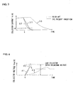
- FIG. 3 is a figure showing the change over time of the collector electrical current (Ic) which flows in said IGBT when the IGBT is turned OFF in the state in which an excessive electrical current has been generated in the collector current.
- the horizontal axis shows time
- the vertical axis shows the magnitude of the collector electrical current (Ic).
- the curved line 31 is the turning OFF curve when turning OFF has been performed by using the drive circuit according to the present invention.
- the curved line 32 is a turning OFF line when the gate resistance value has been made small by a drive circuit according to a prior art technology.
- the curved line 33 is a turning OFF line when the gate resistance value has been made large by a drive circuit according to a prior art technology.
- the turning OFF operation is started at the time point t.
- the rate of reduction with time is controlled to be almost constant until the collector electrical current (Ic) becomes smaller than a, as shown by the curved line 31.
- the rate of reduction of the collector electrical current (Ic) is large after the start of turning OFF, and this rate of reduction becomes smaller along with reduction of the collector electrical current (Ic).
- the rate of reduction of the collector electrical current (Ic) is small, and the time period until the turning OFF operation is completed is long.
- FIG. 4 is a figure showing the rate of change over time of the collector voltage (Vce) of said IGBT when the IGBT is turned OFF in the state in which an excess current (over current) has been generated in the collector electrical current.
- the horizontal axis shows time
- the vertical axis shows the magnitude of the collector voltage (Vce).
- the curved line 41 is the turning OFF curve when turning OFF has been performed by using the drive circuit according to the present invention.
- the curved line 42 is a turning OFF line when the gate resistance value has been made small by a drive circuit according to a prior art technology.
- the curved line 43 is a turning OFF line when the gate resistance value has been made large by a drive circuit according to a prior art technology.
- the turning OFF operation is started at the time point t.
- the time variation (dVce/dt) of the collector voltage is controlled to be almost constant until the collector electrical current (Ic) becomes smaller than a, as shown by the curved line 41.
- the peak of the collector voltage (Vce) shown by the curved line 41 is the smallest among the three curved lines 41 through 43.
- the gate resistance value has been made small with a prior art technology
- the curved line 42 the peak of the collector voltage (Vce) becomes the greatest, since the rate of reduction of the collector electrical current (Ic) is great.
- the time variation (dVce/dt) of the collector voltage becomes gentle, but the time period for the turning OFF operation is long.
- the gain which detects the time variation (dVce/dt) of the collector voltage is determined by the time constant of the capacitor (C101) and the resistor, and when the gain is to be changed over between when the collector electrical current is normal and when it is excessive, it is arranged to change over this detection gain by changing over between the resistor (R102) and the resistor (R103), whose resistance values are different.
- R102 resistor
- R103 resistor
Landscapes
- Power Conversion In General (AREA)
- Electronic Switches (AREA)
Abstract
Description
- The present invention relates to a drive circuit for a voltage driven semiconductor element which supplies a drive electrical current to a load.
- In circuits for switching and driving a voltage driven type semiconductor element such as an insulated gate bipolar transistor (IGBT), there is a per se known technique (refer to Japanese Laid-Open Patent Publication No. H10-51285) of suppressing voltage surges generated when the IGBT which has generated excess electrical current is turned OFF, and the like. In the drive circuit described in that document, the voltage surge is mitigated by suppressing the rate of change of the collector current upon turning OFF by making the resistance value of the gate resistance greater when excess current has been generated in the IGBT.
- Generally a certain dead time is specified for a system to which the drive circuit is fitted, and,it is necessary to turn OFF the IGBT during this dead time. The down side to suppressing the rate of change of the collector current (the rate of its reduction with time) upon turning OFF simply by making the gate resistance value greater as described above, is that the time period until the IGBT is turned OFF becomes undesirably long. In other words, if priority is given to turning OFF the IGBT during the dead time, this puts a limitation upon the magnitude of the gate resistance value. As a result, the suppression of the rate of change of the collector electrical current becomes insufficient. On the other hand, if priority is given to suppressing the rate of change of the collector current, no limitation is imposed upon the size of the gate resistance value. As a result, the time period for turning the IGBT OFF becomes long. Thus, there has been a difficulty in ensuring that suppression of the rate of change of the collector electrical current and shortening of the time period for turning OFF are compatible with one another.
- According to the first aspect of the present invention, a drive circuit for a voltage driven type semiconductor element comprises: an electrical charge supply means for supplying electrical charge to a gate terminal of a voltage driven type semiconductor element when the voltage driven type semiconductor element is turned ON; an electrical charge discharge means for discharging electrical charge from the gate terminal of the voltage driven type semiconductor element when the voltage driven type semiconductor element is turned OFF; and an electrical discharge control means for controlling electric discharge by the electrical charge discharge means so as to bring a rate of reduction with time of the collector electrical current of the voltage driven type semiconductor element, when it is turned OFF, to approach a predetermined value.
- According to the second aspect of the present invention, a drive circuit for a voltage driven type semiconductor element comprises: an electrical charge discharge means for discharging electrical charge from a gate terminal of a voltage driven type semiconductor element when the voltage driven type semiconductor element is turned OFF; and an electrical discharge control means for detecting a time variation of a collector voltage of the voltage driven type semiconductor element, and for controlling electric discharge by the electrical charge discharge means according to the time variation of the collector voltage which has been detected.
- In the above, "unit" may be substituted for "means".
-
- FIG. 1 is a figure for explanation of an IGBT drive circuit according to a preferred embodiment of the present invention.
- FIG. 2 is a figure for explanation of a signal waveform in a main section of the drive circuit.
- FIG. 3 is a figure showing the variation with time of the collector current, when the IGBT which has generated excess current is turned OFF.
- FIG. 4 is a figure showing the variation with time of the collector voltage, when this IGBT which has generated excess current is turned OFF.
-
- In the following, a preferred embodiment for implementing the present invention will be explained with reference to the figures. FIG. 1 is a figure for explanation of a drive circuit for an IGBT (an insulated gate bipolar transistor) according to the preferred embodiment of the present invention. In FIG. 1, to an IGBT (Q101), there are provided a gate terminal (G), a collector terminal (C), an emitter terminal (E) which is connected to an emitter main cell, and a sense terminal (S) which is connected to a cell for detecting the collector current.
- The collector terminal (C) of the IGBT (Q101) is connected to one end of a load (L101), and the other end of the load (L101) is connected to the positive side of a voltage supply VB. The emitter terminal (E) of the IGBT (Q101) is connected to the negative side of the voltage supply VB. When the IGBT (Q101) is ON, a collector current (Ic) in the direction shown in FIG. 1 by the arrow sign flows and drives the load (L101). The parasitic inductance which is present in the electrical current flow path will be supposed to be expressed as (Ls). It should be understood that, in this preferred embodiment, "GNDC" shown in the drawings and written in the specification denotes the electrical potential of the emitter terminal of the IGBT (Q101), while the earth symbol in the figures denotes connection to the emitter terminal of the IGBT (Q101).
- The IGBT (Q101) is made so as to perform switching operation (ON/OFF) according to an input voltage Vin which is supplied from a higher level controller which is not shown in the drawings. Having been impedance converted by a buffer IC (I102), this input voltage (Vin) is inputted to the base terminal of an NPN transistor (Q102) for driving a turning on gate of the IGBT (Q101). This buffer IC (I102) has a push-pull structure.
- The input voltage (Vin) which has been impedance converted by the buffer IC (I102) is furthermore inputted via a resistor (R103) to the base terminal of a PNP transistor (Q103) for driving a turning off gate. The two transistors (Q102) and (Q103) for gate driving described above are connected to the gate terminal (G) of the IGBT (Q101) via respective gate resistors (Rgon) and (Rgoff) which are connected to the respective emitter terminals of these transistors, so as to be able to vary, respectively, the charge current and the discharge current to the gate terminal (G) of the IGBT (Q101). It should be understood that (Vcc) denotes the voltage supply for the circuit.
- The sense terminal (S) of the above described IGBT (Q101) is a terminal which is provided for detecting the collector current of the IGBT (Q101) . This sense terminal (S) is connected to the emitter terminal of the IGBT (Q101) via a sense resistor (R101). A current which bears a predetermined current ratio with respect to the emitter current flowing in the IGBT (Q101) flows in the direction shown by the arrow sign as a sense electrical current (IS). A comparator (I101) compares the voltage which is created between the two ends of this sense resistor (R101) with a threshold value voltage (Vth), and outputs the calculated result of this comparison. The voltage which is created in the sense resistor (R101) is inputted to an inverting input (-) terminal of this comparator (I101), while the threshold value voltage (Vth) is inputted to a non-inverting input (+) terminal of the comparator (I101).
- With the objective of detecting the time variation (dVce/dt) of the collector voltage (Vce) when the IGBT (Q101) is turned OFF, and of feedback controlling the operation of the above described PNP transistor (Q103) for turning OFF, a capacitor (C101) is provided between the collector terminal (C) of the IGBT (Q101) and the base terminal of the PNP transistor (Q103) . Furthermore, with the objective of limiting the amount of feedback detection of this time variation (dVce/dt) of the collector voltage (Vce) in the above described turned OFF state to a predetermined value, an adjusting resistor (R102) is provided between the base terminal of the PNP transistor (Q103) and GNDC. The time variation of the collector voltage may be referred to as the variation with time of the collector voltage or the time base variation of the collector voltage.
- The GNDC side terminal of the adjusting resistor (R102) is connected to GNDC via a Pch-MOSFET (Q105) and a Nch-MOSFET (Q104), which are switching elements, so as to change over the above described feedback detection amount according to the conduction state of the IGBT (Q101). When the Pch-MOSFET (Q105) and the Nch-MOSFET (Q104) are both ON, the GNDC side terminal of the adjusting resistor (R102) is connected to the emitter terminal of the IGBT (Q101), while, when either one of the Pch-MOSFET (Q105) and the Nch-MOSFET (Q104) is turned OFF, the GNDC side terminal of the adjusting resistor (R102) is not thus connected.
- One of the terminals of the adjusting resistor (R103), whose resistance value is different from that of the adjusting resistor (R102) (R102<R103), is connected to the base terminal of the PNP transistor (Q103) in the same manner as the adjusting resistor (R102) , while its other terminal is connected to the output terminal of the buffer IC (I102) and to the gate terminal of the Pch-MOSFET (Q105). The gate terminal of the Nch-MOSFET (Q104) is connected to the output terminal of the above described comparator (I101).
- The output terminal of the comparator (I101), furthermore, along with being connected to the voltage supply (Vcc) via a pull up resistor (R104), is also connected to the gate terminal of a Pch-MOSFET (Q106) which is provided for forcibly controlling the signal level of the input voltage (Vin) to H (High) level. In this preferred embodiment, if the input voltage (Vin) is H level, the IGBT (Q101) is turned OFF. The source terminal of this Pch-MOSFET (Q106) is connected to the voltage supply (Vcc), while its drain terminal is connected to the input terminal of the buffer IC (I102). Furthermore, a capacitor (C102) is provided between the output terminal of the comparator (I101) and GNDC.
- When the output level of the comparator (I101) changes, the operational ON/OFF states of the Pch-MOSFET (Q106) and the Nch-MOSFET (Q104) both change. The output signal of the comparator (I101) is also outputted to the higher level controller (not shown in the figures) as an error signal (110). The higher level controller is made so as, if the error signal shows the occurrence of an abnormality (i.e., in this embodiment, is L (Low) level), to bring the signal (in other words, the input voltage (Vin)) to perform switching control of the IGBT (Q101) to H level (i.e., it turns the IGBT (Q101) OFF). In the case of building an inverter or the like with a plurality of IGBTs, by utilizing as a trigger signal an error signal (110) which shows that an excess electrical current has occurred in any one of the IGBTs, the higher level controller turns OFF all these IGBTs which constitute the inverter or the like.
- The above described capacitor (C102) is provided with the intention of maintaining the output level of the comparator (I101) for a predetermined time period, so that the error signal (110) can be reliably recognized by the higher level controller.
- The operation of the drive circuit described above will now be explained. FIG. 2 is a figure for explanation of the signal waveforms in the main part of the drive circuit of FIG. 1. In FIG. 2, respective waveforms are shown for the collector electrical current (Ic) of the IGBT (Q101) , the input voltage (Vin) , the output voltage of the buffer IC (I102), the voltage (Vce) of the transistor (Q102), the gate voltage (Vge) of the IGBT (Q101), the voltage (Vbe) of the transistor (Q103), the voltage (Vce) of the transistor (Q103) , the electrical current of the capacitor (C101), the voltage between the two ends of the resistor (R102), the voltage between the two ends of the resistor (R103), the collector voltage (Vce) of the IGBT (Q101), the sense terminal electrical current (Is), the output voltage of the comparator (I101), the voltage (Vds) of the MOSFET (Q104), the voltage (Vds) of the MOSFET (Q105), and the voltage (Vds) of the MOSFET (Q106).
- First, the case in which the IGBT (Q101) is turned OFF in the state in which the collector electrical current (Ic) of the IGBT (Q101) is in the proper electrical current range will be explained.
- At the time point t1 of FIG. 2, when the higher level controller (not shown in the drawings) has changed the signal level of the input voltage (Vin) from L (Low) level to H (High) level so that the IGBT (Q101) is turned OFF, the buffer IC (I102) changes the inverted signal after impedance conversion from H level to L level (the output voltage of I102)
- When the output signal of the buffer IC (I102) changes to L level, the NPN transistor (Q102) for driving turning ON gate shifts from the ON state to the OFF state, and the collector voltage (the voltage Q102 Vce) of the NPN transistor (Q102) changes from L level to H level. At the same time as this, a voltage difference (the voltage Q103 Vbe) is generated between the base and the emitter of the PNP transistor (Q103) for driving turning OFF gate which is made of a push-pull structure, and the PNP transistor (Q103) shifts from the OFF state to the ON state. By the PNP transistor (Q103) going to ON, the gate electrical charge within the IGBT (Q101) is discharged via the gate resistor (Rgoff) and the PNP transistor (Q103), and the gate voltage (Vge) of the IGBT (Q101) starts to drop.
- It should be understood that, at this time point, the Pch-MOSFET (Q106) is in the OFF state and the Q106 Vds voltage is H level, the Pch-MOSFET (Q105) is in the ON state and the Q105 Vds voltage is L level, and the Nch-MOSFET (Q104) is in the ON state and the Q104 Vds voltage is L level.
- Along with the dropping of the gate voltage (Vge) of the IGBT (Q101), at the same time as the interruption of the collector electrical current (Ic) of the IGBT (Q101), the collector voltage (Vce) of the IGBT (Q101) starts to rise. The time variation (dVce/dt) of the collector voltage which is rising is detected by differentiating with the capacitor (C101) (the C101 electrical current), and the voltage which is generated between the two ends of the resistor (R102) by the differentiated electrical current which flows in the capacitor (C101) (the voltage across R102) is fed back to the base voltage of the PNP transistor (Q103) for driving turning OFF gate.
- In this case, the voltage Vbe (Q103) between the base and the emitter of the PNP transistor (Q103) for driving turning OFF gate at any time point t is given by the following Equation (1) :
- The second term in the right side of the above Equation (1) is the same as one which gives the time variation of the voltage which is generated between the two ends of said resistor as a transient response equation, when the capacitor and the resistor are connected in series as a differentiation circuit and a voltage change dV/dt which has a predetermined time variation has been inputted to said capacitor.
- The above Equation (1) shows that the voltage Vbe (Q103) between the base and the emitter, which determines the operational state of the PNP transistor (Q103) for driving turning OFF gate, changes linearly when the time variation (dVce/dt) of the collector voltage (Vce) which rises when the IGBT (Q101) is turned OFF changes. As a result of the continuous change of the amount of discharge of the gate electrical charge of the IGBT (Q101) due to the fact that the voltage Vbe (Q103) between the base and the emitter of the PNP transistor (Q103) changes, the time variation (dVce/dt) of the collector voltage of the IGBT (Q101) when turned OFF is feedback controlled to a constant value (D1).
- When, in the state in which the collector electrical current (Ic) of the IGBT (Q101) is within the normal electrical current range, the IGBT (Q101) is turned OFF in this manner, since the time variation (dVce/dt) of the collector voltage is detected by the gain which is determined by the time constant due to the capacitor (C101) and the resistor (R102), accordingly it is possible to perform continuous feedback control of the operational state of the PNP transistor (Q103) for driving turning OFF gate so as to keep the time variation (dVce/dt) of the collector voltage at the constant value (D1).
- During the above described feedback control of the time variation (dVce/dt) of the collector voltage, the time variation (dIc/dt) of the collector electrical current (Ic) of the IGBT (Q101) is kept to a constant value (expressed as d1). As a result, the surge voltage (Vs) which is generated when the IGBT (Q101) is turned OFF is kept to (dIc/dt) x Ls = d1 x Ls. Since the above described feedback control for the time variation (dVce/dt) of the collector voltage operates until directly before the turning OFF of the IGBT (Q101) is completed, it is not influenced by the size of the collector electrical current (Ic) of the IGBT (Q101) , or by deviations in the characteristics of the IGBT (Q101), and the surge voltage (Vs) due to the IGBT (Q101) is suppressed to a small level.
- It should be understood that, since the collector electrical current of the IGBT (Q101) is within the normal electrical current range, the output signal level of the comparator (1101) which is provided for excess electrical current detection is also kept at H level after the time point t1 at which the IGBT (Q101) starts its turning OFF operation. Accordingly, the OFF state of the Pch-MOSFET (Q106) is continued, and the signal level of the input voltage (Vin) from the higher level controller remains, just as it is, at the input signal level of the buffer IC (I102).
- When, at the time point t2, the higher level controller (not shown in the figures) changes the input voltage (Vin) from H level to L level so that the IGBT (Q101) is turned ON, the buffer IC (I102) changes the inverted signal after impedance conversion from L level to H level (the I102 output voltage).
- When the output level of the buffer IC (I102) changes to H level, the NPN transistor (Q102) for driving turning ON gate shifts from the OFF state to the ON state, and the collector voltage of the NPN transistor (Q102) (the voltage Q102 Vce) changes from H level to L level. At the same time as this, the Pch-MOSFET (Q105) shifts from the ON state to the OFF state, and the voltage Q105 Vds changes from L level to H level. The Pch-MOSFET (Q105) is a switching element which is required for turning the PNP transistor (Q103) for driving turning OFF gate of the IGBT (Q101) to OFF. In other words, by the Pch-MOSFET (Q105) going to OFF, the base terminal of the PNP transistor (Q103) for driving turning OFF gate is connected (pulled up) via the resistor (R103) to the H level of the output of the buffer IC (I102) at this time point. By doing this, the PNP transistor (Q103) for driving turning OFF gate is reliably turned OFF, and the voltage Q103 Vce becomes H level.
- Next, the case in which the IGBT (Q101) is turned OFF in the state in which the collector electrical current of the IGBT (Q101) has become excessive will be explained.
- A sense terminal electrical current (Is) flows to the resistor (R101) from the sense terminal (S) of the IGBT (Q101) according to the collector electrical current (Ic) of the IGBT (Q101) which is turned ON. The IGBT (Q101) is made so that the ratio of its sense terminal electrical current (Is) and its collector electrical current (Ic) has a predetermined electrical current ratio (which is determined by the device structure of the IGBT).
- When the voltage which is generated between the two ends of the resistor (R101) by this sense terminal electrical current (Is) exceeds the threshold voltage value (Vth) at the time point t3 (in other words, when the collector electrical current (Ic) exceeds its permitted value), the calculated comparison output of the comparator (I101) changes from H level to L level. When the output signal of the comparator (I101) changes to L level, the Pch-MOSFET (Q106) shifts from the OFF state to the ON state, and the voltage Q106 Vds goes to L level. Due to this, the IGBT (Q101) is shifted to OFF operation, even if the signal level of the input voltage (Vin) from the higher level controller is at L level, since the input signal of the buffer IC (I102) is connected to the voltage supply (Vcc) (i. e. goes to H level) due to the Pch-MOSFET (Q106) going to ON.
- The buffer IC (I102) changes the inverted signal after impedance conversion from H level to L level (the voltage output from I102). When the output signal of the buffer IC (I102) changes to L level, the NPN transistor (Q102) for driving turning ON gate shifts from the ON state to the OFF state, and the collector voltage of this NPN transistor (Q102) (the voltage Q102 Vce) changes from L level to H level. At the same time as this, a voltage difference (the voltage Q103 Vbe) is generated between the base and the emitter of the PNP transistor (Q103) for driving turning off gate which is made of a push-pull structure, and this PNP transistor (Q103) shifts from the OFF state to the ON state. Due to the PNP transistor (Q103) going to ON, the gate electrical charge within the IGBT (Q101) is discharged via the gate resistor (Rgoff) and the PNP transistor (Q103), and the gate voltage (Vge) of the IGBT (Q101) starts to drop.
- At this time point, with the Pch-MOSFET (Q106) in the ON state the voltage Q106 Vds is L level, with the Pch-MOSFET (Q105) in the ON state the voltage Q105 Vds is L level, and with the Nch-MOSFET (Q104) in the OFF state the voltage Q104 Vds is H level
- At the same time as the collector electrical current (Ic) of the IGBT (Q101) is interrupted along with the dropping of the gate voltage (Vge) of the IGBT (Q101), the collector voltage (Vce) of the IGBT (Q101) starts to rise. The time variation (dVce/dt) of the collector voltage which is rising is detected by differentiating with the capacitor (C101) (the C101 electrical current), and the voltage which is generated between the two ends of the resistor (R103) by the differential electrical current which flows in the capacitor (C101) (i.e. the voltage across R103) is fed back to the base voltage of the PNP transistor (Q103) for driving turning OFF gate.
- In this case, the voltage Vbe (Q103)' between the base and the emitter of the PNP transistor for driving turning OFF gate at any time point t is given by the following Equation (2):
- Since the detected gain of the time variation (dVce/dt') of the collector voltage of the IGBT (Q101) is changed over to the detection gain if the collector electrical current described above is in the normal range and is fed back to the base voltage of the PNP transistor (Q103) for driving turning OFF gate, accordingly the time variation (dVce/dt') of the collector voltage of the IGBT (Q101) comes to be changed over to the constant value (D2). When the detected gain of the time variation (dVce/dt') of the collector voltage becomes high, the feedback amount to the base voltage of the PNP transistor (Q103) increases and the electrical charge discharge speed becomes slow. Conversely, if the detected gain is low, the electrical charge discharge speed due to the PNP transistor (Q103) becomes high. In this preferred embodiment, the electrical charge discharge speed is controlled by changing over the detection gain between when the collector electrical current is normal and when it is abnormal (i.e. during excess electrical current).
- Even if the IGBT (Q101) is turned OFF in the state in which excess electrical current has been generated in the collector current, in the same way as when it is turned OFF in the state in which the collector electrical current is in the normal range, it is possible to suppress the surge voltage (Vs), since the above described feedback control operates until directlybefore the turning OFF of the IGBT (Q101) is completed.
- The IGBT (Q101) turns OFF when the discharge of the gate electrical charge via the gate resistor (Rgoff) and the PNP transistor (Q103) is completed (i.e. when the gate voltage (Vge) becomes zero). On the other hand, the higher level controller (not shown in the drawings) which has received the error signal (110) changes the input voltage (Vin) from L level to H level at a predetermined timing after the time point t3.
- The values of the time variation of the collector voltage (dVce/dt) = D1 and (dVce/dt') = D2 are determined during the design process, so that the respective surge voltages (Vs) do not exceed a predetermined range (the rated breakdown voltage of the IGBT (Q101)). The values of D1 and D2 are determined by the resistance values of the respective resistors (R102) and (R103).
- FIG. 3 is a figure showing the change over time of the collector electrical current (Ic) which flows in said IGBT when the IGBT is turned OFF in the state in which an excessive electrical current has been generated in the collector current. In FIG. 3, the horizontal axis shows time, and the vertical axis shows the magnitude of the collector electrical current (Ic). The
curved line 31 is the turning OFF curve when turning OFF has been performed by using the drive circuit according to the present invention. Thecurved line 32 is a turning OFF line when the gate resistance value has been made small by a drive circuit according to a prior art technology. And thecurved line 33 is a turning OFF line when the gate resistance value has been made large by a drive circuit according to a prior art technology. - In FIG. 3, the turning OFF operation is started at the time point t. With the drive circuit according to the present invention, the rate of reduction with time is controlled to be almost constant until the collector electrical current (Ic) becomes smaller than a, as shown by the
curved line 31. In the case that the gate resistance value has been made small with a prior art technology, as shown by thecurved line 32, the rate of reduction of the collector electrical current (Ic) is large after the start of turning OFF, and this rate of reduction becomes smaller along with reduction of the collector electrical current (Ic). And, in the case that the gate resistance value has been made large with a prior art technology, as shown by thecurved line 33, the rate of reduction of the collector electrical current (Ic) is small, and the time period until the turning OFF operation is completed is long. - FIG. 4 is a figure showing the rate of change over time of the collector voltage (Vce) of said IGBT when the IGBT is turned OFF in the state in which an excess current (over current) has been generated in the collector electrical current. In FIG. 4, the horizontal axis shows time, and the vertical axis shows the magnitude of the collector voltage (Vce). The
curved line 41 is the turning OFF curve when turning OFF has been performed by using the drive circuit according to the present invention. Thecurved line 42 is a turning OFF line when the gate resistance value has been made small by a drive circuit according to a prior art technology. And thecurved line 43 is a turning OFF line when the gate resistance value has been made large by a drive circuit according to a prior art technology. - In FIG. 4, the turning OFF operation is started at the time point t. With the drive circuit according to the present invention, the time variation (dVce/dt) of the collector voltage is controlled to be almost constant until the collector electrical current (Ic) becomes smaller than a, as shown by the
curved line 41. The peak of the collector voltage (Vce) shown by thecurved line 41 is the smallest among the threecurved lines 41 through 43. In the case that the gate resistance value has been made small with a prior art technology, as shown by thecurved line 42, the peak of the collector voltage (Vce) becomes the greatest, since the rate of reduction of the collector electrical current (Ic) is great. And, in the case that the gate resistance value has been made large with a prior art technology, as shown by thecurved line 43, the time variation (dVce/dt) of the collector voltage becomes gentle, but the time period for the turning OFF operation is long. - As is clear from FIGS. 3 and 4, with the drive circuit according to the present invention, it is possible to suppress the peaks of the collector voltage (Vce) , with the time period for turning OFF not becoming protracted by increasing the gate resistance value.
- The preferred embodiment explained above will now be summarized.
- (1) With the drive circuit according to the present invention, when the IGBT (Q101) is turned ON, electrical charge is supplied (charging) from the gate terminal (G) via the resistor (Rgon) by the NPN transistor (Q102) for driving turning ON gate being turned ON; while, when the IGBT (Q101) is turned OFF, electrical charge is discharged from the gate terminal (G) via the resistor (Rgoff) by the PNP transistor (Q103) for driving turning OFF gate being turned OFF.
- (2) The ON state of the PNP transistor (Q103) for driving turning OFF gate controls feedback according to the time variation (dVce/dt) of the collector voltage of the IGBT (Q101). Accordingly, it is possible to vary the amount of electrical discharge of the gate electrical charge which is discharged from the gate terminal (G) linearly along with the time variation (dVce/dt) of the collector voltage, and it is possible to control the time variation (dVce/dt) of the collector voltage to a constant value (D1 or D2). By doing this, it is possible to make the time variation (dIc/dt) of the collector electrical current (Ic) roughly constant, and, even during excess electrical current, there is no generation of excessively large surge voltage, and it is possible to turn the IGBT (Q101) OFF in a short period of time (i.e., quickly) .
- (3) By performing the feedback control according to the time variation (dVce/dt) of the collector voltage, it becomes difficult to experience any influence from deviations of the characteristics of the IGBT (Q101), or from parasitic inductance (Ls) in the collector electrical current transmission path (the bus bars or the like). Due to this, it is possible to performing turning OFF switching so as to keep the surge voltage within a fixed value, irrespective of variation of the characteristics and of the parasitic inductance value.
- (4) By arranging that no excessively large surge voltage is generated in the IGBT (Q101), it becomes possible to make the IGBT (Q101) using elements of which the rated breakdown voltage (the collector withstand voltage) is low, and thus it is possible to reduce the size of the IGBT. Furthermore, since it is possible for the IGBT collector saturation voltage to be low, it is also possible to restrict the losses which are generated by the IGBT.
-
- In the above explanation, the gain which detects the time variation (dVce/dt) of the collector voltage is determined by the time constant of the capacitor (C101) and the resistor, and when the gain is to be changed over between when the collector electrical current is normal and when it is excessive, it is arranged to change over this detection gain by changing over between the resistor (R102) and the resistor (R103), whose resistance values are different. Instead of this, it would also be acceptable to provide a capacitor (C102) whose capacitance was different from the capacitance of the capacitor (C101), and to change over the detection gain by changing over between the capacitor (C101) and the capacitor (C102).
- Instead of changing over between the capacitor (C101) and the capacitor (C102), it would also be acceptable to connect the capacitor (C102) in parallel with the capacitor (C101), and to change the detected gain by cutting out this parallel connected capacitor (C102).
- The above described embodiments are examples, and various modifications can be made without departing from the spirit and scope of the invention.
Claims (13)
- A drive circuit for a voltage driven type semiconductor element, comprising:an electrical charge supply means (Q102, Rgon) for supplying electrical charge to a gate terminal of a voltage driven type semiconductor element when the voltage driven type semiconductor element is turned ON;an electrical charge discharge means (Q103, Rgoff) for discharging electrical charge from the gate terminal of the voltage driven type semiconductor element when the voltage driven type semiconductor element is turned OFF; andan electrical discharge control means (C101, R102, R103) for controlling electric discharge by the electrical charge discharge means (Q103, Rgoff) so as to bring a rate of reduction with time of the collector electrical current of the voltage driven type semiconductor element, when it is turned OFF, to approach a predetermined value.
- A drive circuit for a voltage driven type semiconductor element, comprising:an electrical charge discharge means (Q103, Rgoff) for discharging electrical charge from a gate terminal of a voltage driven type semiconductor element when the voltage driven type semiconductor element is turned OFF; andan electrical discharge control means (C101, R102, R103) for detecting a time variation of a collector voltage of the voltage driven type semiconductor element, and for controlling electric discharge by the electrical charge discharge means (Q103, Rgoff) according to the time variation of the collector voltage which has been detected.
- A drive circuit for a voltage driven type semiconductor element according to claim 2, further comprising:an electrical current detection means (R101, I101) for detecting a collector electrical current of the voltage driven type semiconductor element, and whereinthe electrical discharge control means (C101, R102, R103) varies a discharge speed by the electrical charge discharge means (Q103, Rgoff) according to the electrical current value which has been deterted by the electrical current detection means (R101, I101).
- A drive circuit for a voltage driven type semiconductor element according to claim 3, wherein:the electrical discharge control means (C101, R102, R103) comprises a differentiation circuit which comprises a resistor element and a capacitor element, and which differentiates the variation of the collector voltage of the voltage driven type semiconductor element;the electrical charge discharge means (Q103, Rgoff) comprises a PNP transistor, whose emitter terminal is connected to the gate terminal of the voltage driven type semiconductor element, and whose collector terminal is connected to an emitter terminal of the voltage driven type semiconductor element; anda differentiated output from the differentiation circuit is inputted to a base terminal of the PNP transistor.
- A drive circuit for a voltage driven type semiconductor element according to claim 4, wherein:the resistor element of the differentiation circuit comprises a first resistor element which has a first resistance value, and a second resistance element which has a second resistance value which is greater than the first resistance value, which can be optionally changed over; andthe electrical discharge control means (C101, R102, R103) changes over to the first resistor element when the electrical current value which is detected by the electrical current detection means (R101, I101) is less than or equal to a predetermined value, and changes over to the second resistor element when the electrical current value which is detected by the electrical current detection means (R101, I101) is greater than the predetermined value.
- A drive circuit for a voltage driven type semiconductor element according to claim 2, further comprising:an electrical charge supply means (Q102, Rgon) for supplying electrical charge to a gate terminal of the voltage driven type semiconductor element when the voltage driven type semiconductor element is turned ON;the electrical charge supply means (Q102, Rgon) comprising an NPN transistor;the electrical charge discharge means (Q103, Rgoff) comprising a PNP transistor;a signal output circuit which has a push-pull structure, and which outputs a drive signal to a base terminal of the NPN transistor;a capacitance element, a first resistor element, and a first switching element which are connected between the collector terminal and the emitter terminal of the voltage driven type semiconductor element, and are connected in series; anda second resistor element of which one terminal is connected to a connection point of the capacitance element and the first resistor element, and the other terminal is connected to an output terminal of the signal output circuit, wherein:the connection point of the capacitance element, the first resistor element, and the second resistance element is connected to a base terminal of the PNP transistor; anda time constant due to the capacitance element and the first resistor element, and a time constant due to the capacitance element and the second resistor element, are changed over between according to a switching state of the first switching element.
- A drive circuit for a voltage driven type semiconductor element according to claim 6, further comprising:a second switching element which is connected in series between the first resistor element and the first switching element, and which is changed over according to an output signal level from the signal output circuit, and whereinthe second switching element is turned ON to cause the PNP transistor to operate, by the output signal which is outputted from the signal output circuit when the voltage driven type semiconductor element is turned OFF.
- A drive circuit for a voltage driven type semiconductor element according to claim 2 or claim 3, wherein
the electrical discharge control means (C101, R102, R103) controls electrical discharge by the electrical charge discharge means (Q103, Rgoff) so as to bring a rate of reduction with time of the collector electrical current of the voltage driven type semiconductor element to approach a predetermined value. - A drive circuit for a voltage driven type semiconductor element according to claim 2 or claim 3, wherein
the electrical discharge control means (C101, R102, R103) controls electrical discharge by the electrical charge discharge means (Q103, Rgoff) so that the time variation of the collector voltage becomes constant. - A drive circuit for a voltage driven type semiconductor element according to claim 3, wherein
when the electrical current value which is detected by the electrical current detection means (R101, I101) is greater than or equal to a predetermined value, the electrical discharge controlmeans (C101, R102, R103) controls electrical discharge by the electrical charge discharge means (Q103, Rgoff) so that the electrical discharge speed is slower, than when the electrical current value is less than the predetermined value. - A drive circuit for a voltage driven type semiconductor element according to claim 3, wherein
the electrical discharge control means (C101, R102, R103) controls electrical discharge by the electrical charge discharge means (Q103, Rgoff) so as to make the time variation of the collector voltage constant, and, when the electrical current value which is detected by the electrical current detection means (R101, I101) is greater than or equal to a predetermined value, controls electrical discharge by the electrical charge discharge means (Q103, Rgoff) so as to make the time variation of the collector voltage smaller, than when the electrical current value is less than the predetermined value. - A drive circuit for a voltage driven type semiconductor element according to claim 2, wherein
the electrical discharge control means (C101, R102, R103) comprises a differentiation circuit which detects the time variation of the collector voltage and feeds back the detected time variation to the electrical charge discharge means (Q103, Rgoff). - A drive circuit for a voltage driven type semiconductor element according to claim 3, wherein
the electrical discharge control means (C101, R102, R103) comprises a differentiation circuit which detects the time variation of the collector voltage and feeds back the detected time variation to the electrical charge discharge means (Q103, Rgoff), and varies the discharge speed by the electrical charge discharge means (Q103, Rgoff) by changing over a resistor element which constitutes the differentiation circuit, according to the electrical current value which is detected by the electrical current detection means (R101, I101).
Applications Claiming Priority (2)
| Application Number | Priority Date | Filing Date | Title |
|---|---|---|---|
| JP2004081571 | 2004-03-19 | ||
| JP2004081571A JP4144541B2 (en) | 2004-03-19 | 2004-03-19 | Driver circuit for voltage-driven semiconductor device |
Publications (2)
| Publication Number | Publication Date |
|---|---|
| EP1580888A1 true EP1580888A1 (en) | 2005-09-28 |
| EP1580888B1 EP1580888B1 (en) | 2008-08-20 |
Family
ID=34858358
Family Applications (1)
| Application Number | Title | Priority Date | Filing Date |
|---|---|---|---|
| EP05005399A Ceased EP1580888B1 (en) | 2004-03-19 | 2005-03-11 | Drive circuit for voltage driven type semiconductor element |
Country Status (6)
| Country | Link |
|---|---|
| US (1) | US7242238B2 (en) |
| EP (1) | EP1580888B1 (en) |
| JP (1) | JP4144541B2 (en) |
| KR (1) | KR100627126B1 (en) |
| CN (1) | CN1671049B (en) |
| DE (1) | DE602005009054D1 (en) |
Cited By (1)
| Publication number | Priority date | Publication date | Assignee | Title |
|---|---|---|---|---|
| WO2024089263A1 (en) * | 2022-10-27 | 2024-05-02 | Inventronics Gmbh | Circuit arrangement for controlling a load |
Families Citing this family (49)
| Publication number | Priority date | Publication date | Assignee | Title |
|---|---|---|---|---|
| JP4742828B2 (en) | 2005-11-18 | 2011-08-10 | 日産自動車株式会社 | Voltage-driven switching circuit |
| JP4622875B2 (en) * | 2006-02-07 | 2011-02-02 | 株式会社デンソー | Communication driver circuit |
| JP4967568B2 (en) * | 2006-09-26 | 2012-07-04 | 日産自動車株式会社 | Gate drive circuit for voltage driven element |
| KR100807541B1 (en) * | 2006-09-29 | 2008-02-29 | 엘에스산전 주식회사 | Gate driving circuit of power semiconductor switch |
| KR100807547B1 (en) | 2006-12-28 | 2008-03-03 | 엘에스산전 주식회사 | Drive circuit of semiconductor switch for inverter |
| JP4752811B2 (en) * | 2007-06-06 | 2011-08-17 | 日産自動車株式会社 | Drive circuit for voltage-driven element |
| DE102007040783A1 (en) * | 2007-08-28 | 2009-03-12 | Conti Temic Microelectronic Gmbh | Method for controlling non-linear load elements |
| US8503146B1 (en) * | 2007-10-16 | 2013-08-06 | Fairchild Semiconductor Corporation | Gate driver with short-circuit protection |
| KR100967781B1 (en) | 2008-04-10 | 2010-07-05 | 엘에스산전 주식회사 | Drive circuit of switching element in inverter |
| JP5003596B2 (en) * | 2008-05-30 | 2012-08-15 | 三菱電機株式会社 | Power element drive circuit |
| EP2197111B1 (en) * | 2008-12-15 | 2012-06-20 | Danaher Motion Stockholm AB | A gate driver circuit, switch assembly and switch system |
| CN101752841B (en) * | 2008-12-19 | 2012-08-22 | 比亚迪股份有限公司 | Insulated gate bipolar transistor (IGBT) protection circuit and motor control system |
| JP5477264B2 (en) * | 2010-11-26 | 2014-04-23 | 株式会社デンソー | Communication driver circuit |
| JP5430608B2 (en) * | 2011-04-27 | 2014-03-05 | カルソニックカンセイ株式会社 | Semiconductor switching element drive circuit |
| CN102801287B (en) * | 2011-05-25 | 2016-01-20 | 深圳市科陆驱动技术有限公司 | A kind of power device drives pressure limiting circuit |
| JP5464196B2 (en) * | 2011-11-18 | 2014-04-09 | 株式会社デンソー | Power semiconductor element drive circuit |
| CN102412711A (en) * | 2011-11-22 | 2012-04-11 | 常熟市董浜镇华进电器厂 | High-speed driving circuit of power MOS tube |
| US8624637B2 (en) * | 2012-02-08 | 2014-01-07 | Infineon Technologies Ag | Switching control circuit for thermal protection of transistors |
| US8717069B2 (en) * | 2012-04-24 | 2014-05-06 | General Electric Company | Converter switch apparatus and method |
| JP5716711B2 (en) * | 2012-07-20 | 2015-05-13 | 株式会社デンソー | Switching element drive circuit |
| JP5720641B2 (en) * | 2012-08-21 | 2015-05-20 | 株式会社デンソー | Switching module |
| JP5712986B2 (en) * | 2012-08-28 | 2015-05-07 | 株式会社デンソー | Drive circuit for switching element to be driven |
| CN103178694B (en) * | 2013-03-01 | 2015-01-21 | 南京埃斯顿自动控制技术有限公司 | Insulated gate bipolar transistor gate driving push-pull circuit |
| JP5880494B2 (en) * | 2013-07-04 | 2016-03-09 | 株式会社デンソー | Switching control circuit |
| JP5979570B2 (en) * | 2013-07-10 | 2016-08-24 | パナソニックIpマネジメント株式会社 | Semiconductor device and inverter using the same |
| US9094005B2 (en) | 2013-07-30 | 2015-07-28 | Denso Corporation | Semiconductor element module and gate drive circuit |
| KR20160086345A (en) * | 2013-11-14 | 2016-07-19 | 티엠4 인코포레이티드 | Commutation cell, power converter and compensation circuit having dynamically controlled voltage gains |
| JP6504832B2 (en) | 2014-01-28 | 2019-04-24 | ゼネラル・エレクトリック・カンパニイ | Integrated mounting and cooling devices, electronic devices and vehicles |
| DE102014202610B4 (en) * | 2014-02-13 | 2025-06-05 | Robert Bosch Gmbh | Current detection device and method for detecting an electric current |
| JP6187428B2 (en) * | 2014-03-27 | 2017-08-30 | 株式会社デンソー | Drive device |
| JP6396730B2 (en) * | 2014-09-19 | 2018-09-26 | ルネサスエレクトロニクス株式会社 | Semiconductor device |
| JP6652561B2 (en) * | 2014-10-24 | 2020-02-26 | 日本テキサス・インスツルメンツ合同会社 | Adaptive controller for voltage converter |
| US10073512B2 (en) | 2014-11-19 | 2018-09-11 | General Electric Company | System and method for full range control of dual active bridge |
| EP3229373A1 (en) * | 2016-04-06 | 2017-10-11 | Volke Andreas | Soft shutdown modular circuitry for power semiconductor switches |
| JP2017212870A (en) * | 2016-05-20 | 2017-11-30 | 株式会社デンソー | Driving control device for switching element |
| JP6840695B2 (en) | 2018-03-21 | 2021-03-10 | 株式会社東芝 | Semiconductor devices, power converters, drives, vehicles, and elevators |
| CN108964643A (en) * | 2018-06-27 | 2018-12-07 | 深圳市汇北川电子技术有限公司 | A kind of drive control circuit and control method of the power device at current mirror end |
| EP3618278A1 (en) * | 2018-08-28 | 2020-03-04 | Siemens Aktiengesellschaft | Driving of a bipolar transistor having insulated gate electrode |
| US10756726B2 (en) * | 2018-10-01 | 2020-08-25 | Texas Instruments Incorporated | Systems with power transistors, transistors coupled to the gates of the power transistors, and capacitive dividers coupled to the power transistors |
| CN109802662B (en) * | 2018-12-21 | 2023-08-01 | 中国人民解放军空军工程大学 | A system and method for realizing multi-channel discharge on semiconductor surface |
| WO2020144951A1 (en) * | 2019-01-10 | 2020-07-16 | 富士電機株式会社 | Gate drive device, switching device |
| CN110224688A (en) * | 2019-05-08 | 2019-09-10 | 吉林大学 | A kind of gallium nitride power device drive system |
| US11206016B2 (en) * | 2019-09-27 | 2021-12-21 | Analog Devices International Unlimited Company | Gate driver with pulsed gate slew control |
| US11489521B2 (en) * | 2020-01-20 | 2022-11-01 | Fast SiC Semiconductor Incorporated | Power transistor module and controlling method thereof |
| DE112020006675T5 (en) * | 2020-02-04 | 2022-11-24 | Mitsubishi Electric Corporation | power semiconductor device |
| JP7264094B2 (en) * | 2020-03-16 | 2023-04-25 | 株式会社豊田自動織機 | Driver circuit and power converter |
| JP7528744B2 (en) | 2020-11-27 | 2024-08-06 | 株式会社デンソー | Gate Driver |
| KR102677618B1 (en) * | 2022-09-21 | 2024-06-20 | 주식회사 현대케피코 | Igbt device protection circuit, igbt device driving system includign the same, operating method of the igbt device protection circuit |
| WO2025196913A1 (en) * | 2024-03-18 | 2025-09-25 | 日産自動車株式会社 | Electric vehicle heat management method and electric vehicle heat management system |
Citations (2)
| Publication number | Priority date | Publication date | Assignee | Title |
|---|---|---|---|---|
| JP2003070233A (en) * | 2001-08-27 | 2003-03-07 | Toshiba Corp | Gate drive circuit |
| US20030075748A1 (en) * | 2001-10-19 | 2003-04-24 | Mitsubishi Denki Kabushiki Kaisha | Semiconductor device and method of driving transistors |
Family Cites Families (18)
| Publication number | Priority date | Publication date | Assignee | Title |
|---|---|---|---|---|
| DE68925163T2 (en) * | 1988-08-12 | 1996-08-08 | Hitachi Ltd | Insulated gate transistor driver circuit; and their use in a switching circuit, a current switching device, and an induction motor system |
| JPH04278714A (en) * | 1991-03-06 | 1992-10-05 | Toshiba Corp | Igbt driving circuit |
| JPH05336732A (en) * | 1992-06-02 | 1993-12-17 | Toshiba Corp | IGBT gate circuit |
| JP3141613B2 (en) * | 1993-03-31 | 2001-03-05 | 株式会社日立製作所 | Method and circuit for driving voltage-driven element |
| JPH06291361A (en) | 1993-03-31 | 1994-10-18 | Mitsubishi Electric Corp | Optical nonlinear element |
| JP3123349B2 (en) * | 1994-06-29 | 2001-01-09 | 富士電機株式会社 | Control circuit for semiconductor device |
| JPH1051285A (en) * | 1996-05-28 | 1998-02-20 | Mitsubishi Electric Corp | Driver circuit for voltage-controlled transistor |
| EP0814564A1 (en) * | 1996-06-20 | 1997-12-29 | ANSALDO INDUSTRIA S.p.A. | Electronic switching circuit with reduction of switching transients |
| JP3132648B2 (en) * | 1996-09-20 | 2001-02-05 | 富士電機株式会社 | Gate drive circuit in power converter |
| US6127746A (en) * | 1996-10-21 | 2000-10-03 | International Rectifier Corp. | Method of controlling the switching DI/DT and DV/DT of a MOS-gated power transistor |
| JP3462032B2 (en) * | 1997-03-04 | 2003-11-05 | 株式会社東芝 | Power converter |
| WO2000046924A1 (en) * | 1999-02-05 | 2000-08-10 | Koninklijke Philips Electronics N.V. | Driving a switching transistor |
| JP2000324801A (en) | 1999-05-11 | 2000-11-24 | Fuji Electric Co Ltd | Driver circuit for voltage-controlled semiconductor device |
| JP3736227B2 (en) * | 1999-09-20 | 2006-01-18 | 富士電機デバイステクノロジー株式会社 | Drive circuit |
| JP4350295B2 (en) * | 2000-10-26 | 2009-10-21 | 三菱電機株式会社 | Semiconductor device and semiconductor device module |
| JP3812353B2 (en) * | 2001-03-19 | 2006-08-23 | 株式会社日立製作所 | Semiconductor power converter |
| JP3649154B2 (en) | 2001-05-31 | 2005-05-18 | 日産自動車株式会社 | Overcurrent protection device |
| JP2004088192A (en) | 2002-08-23 | 2004-03-18 | Nissan Motor Co Ltd | Drive circuit for voltage drive element |
-
2004
- 2004-03-19 JP JP2004081571A patent/JP4144541B2/en not_active Expired - Fee Related
-
2005
- 2005-03-11 DE DE602005009054T patent/DE602005009054D1/en not_active Expired - Lifetime
- 2005-03-11 EP EP05005399A patent/EP1580888B1/en not_active Ceased
- 2005-03-11 US US11/077,208 patent/US7242238B2/en not_active Expired - Lifetime
- 2005-03-18 CN CN2005100563657A patent/CN1671049B/en not_active Expired - Fee Related
- 2005-03-18 KR KR1020050022796A patent/KR100627126B1/en not_active Expired - Fee Related
Patent Citations (2)
| Publication number | Priority date | Publication date | Assignee | Title |
|---|---|---|---|---|
| JP2003070233A (en) * | 2001-08-27 | 2003-03-07 | Toshiba Corp | Gate drive circuit |
| US20030075748A1 (en) * | 2001-10-19 | 2003-04-24 | Mitsubishi Denki Kabushiki Kaisha | Semiconductor device and method of driving transistors |
Non-Patent Citations (1)
| Title |
|---|
| PATENT ABSTRACTS OF JAPAN vol. 2003, no. 07 3 July 2003 (2003-07-03) * |
Cited By (1)
| Publication number | Priority date | Publication date | Assignee | Title |
|---|---|---|---|---|
| WO2024089263A1 (en) * | 2022-10-27 | 2024-05-02 | Inventronics Gmbh | Circuit arrangement for controlling a load |
Also Published As
| Publication number | Publication date |
|---|---|
| JP4144541B2 (en) | 2008-09-03 |
| JP2005269446A (en) | 2005-09-29 |
| US20050206438A1 (en) | 2005-09-22 |
| KR20060044433A (en) | 2006-05-16 |
| EP1580888B1 (en) | 2008-08-20 |
| KR100627126B1 (en) | 2006-09-25 |
| DE602005009054D1 (en) | 2008-10-02 |
| CN1671049A (en) | 2005-09-21 |
| US7242238B2 (en) | 2007-07-10 |
| CN1671049B (en) | 2010-12-08 |
Similar Documents
| Publication | Publication Date | Title |
|---|---|---|
| EP1580888B1 (en) | Drive circuit for voltage driven type semiconductor element | |
| US10224920B2 (en) | Soft shutdown modular circuitry for power semiconductor switches | |
| US7710187B2 (en) | Gate drive circuit | |
| JP5761215B2 (en) | Gate drive circuit | |
| US9698654B2 (en) | Soft shutdown for isolated drivers | |
| JP3886876B2 (en) | Power semiconductor element drive circuit | |
| EP3035532B1 (en) | Gate drive circuit and method of operating same | |
| US7151401B2 (en) | Semiconductor apparatus | |
| US10084390B2 (en) | Power converter, short circuit protection circuit, and control method | |
| US7514967B2 (en) | Driver for voltage driven type switching element | |
| CN101820276B (en) | Control method and the gate drivers of IGBT | |
| CN107659295B (en) | Isolated gate driver and power device drive system including the same | |
| JP2018011467A (en) | Gate drive circuit for semiconductor switching element | |
| CN111464007A (en) | Method and system for restraining peak voltage at turn-off instant of full-control power switch device | |
| CN113169659B (en) | Driving circuit for power semiconductor element and power semiconductor module using same | |
| JP7226099B2 (en) | gate drive circuit | |
| US9628073B2 (en) | Current control circuit | |
| JP4779549B2 (en) | A gate driving circuit of a voltage driven semiconductor element. | |
| CN114726194A (en) | Power electronic converter and driving circuit board thereof | |
| JP4967568B2 (en) | Gate drive circuit for voltage driven element | |
| JP2014222991A (en) | Inverter controller | |
| US20230053929A1 (en) | Driving apparatus | |
| US20220209645A1 (en) | Driving apparatus | |
| CN121729825A (en) | Gate driving device | |
| CN116073631A (en) | Driving device, driving method and power conversion device |
Legal Events
| Date | Code | Title | Description |
|---|---|---|---|
| PUAI | Public reference made under article 153(3) epc to a published international application that has entered the european phase |
Free format text: ORIGINAL CODE: 0009012 |
|
| 17P | Request for examination filed |
Effective date: 20050311 |
|
| AK | Designated contracting states |
Kind code of ref document: A1 Designated state(s): AT BE BG CH CY CZ DE DK EE ES FI FR GB GR HU IE IS IT LI LT LU MC NL PL PT RO SE SI SK TR |
|
| AX | Request for extension of the european patent |
Extension state: AL BA HR LV MK YU |
|
| AKX | Designation fees paid |
Designated state(s): DE FR GB |
|
| 17Q | First examination report despatched |
Effective date: 20060918 |
|
| GRAP | Despatch of communication of intention to grant a patent |
Free format text: ORIGINAL CODE: EPIDOSNIGR1 |
|
| GRAS | Grant fee paid |
Free format text: ORIGINAL CODE: EPIDOSNIGR3 |
|
| GRAA | (expected) grant |
Free format text: ORIGINAL CODE: 0009210 |
|
| AK | Designated contracting states |
Kind code of ref document: B1 Designated state(s): DE FR GB |
|
| REG | Reference to a national code |
Ref country code: GB Ref legal event code: FG4D |
|
| REF | Corresponds to: |
Ref document number: 602005009054 Country of ref document: DE Date of ref document: 20081002 Kind code of ref document: P |
|
| PLBE | No opposition filed within time limit |
Free format text: ORIGINAL CODE: 0009261 |
|
| STAA | Information on the status of an ep patent application or granted ep patent |
Free format text: STATUS: NO OPPOSITION FILED WITHIN TIME LIMIT |
|
| 26N | No opposition filed |
Effective date: 20090525 |
|
| REG | Reference to a national code |
Ref country code: FR Ref legal event code: PLFP Year of fee payment: 12 |
|
| REG | Reference to a national code |
Ref country code: FR Ref legal event code: PLFP Year of fee payment: 13 |
|
| REG | Reference to a national code |
Ref country code: FR Ref legal event code: PLFP Year of fee payment: 14 |
|
| PGFP | Annual fee paid to national office [announced via postgrant information from national office to epo] |
Ref country code: DE Payment date: 20190226 Year of fee payment: 15 Ref country code: GB Payment date: 20190306 Year of fee payment: 15 |
|
| PGFP | Annual fee paid to national office [announced via postgrant information from national office to epo] |
Ref country code: FR Payment date: 20190213 Year of fee payment: 15 |
|
| REG | Reference to a national code |
Ref country code: DE Ref legal event code: R119 Ref document number: 602005009054 Country of ref document: DE |
|
| PG25 | Lapsed in a contracting state [announced via postgrant information from national office to epo] |
Ref country code: DE Free format text: LAPSE BECAUSE OF NON-PAYMENT OF DUE FEES Effective date: 20201001 Ref country code: FR Free format text: LAPSE BECAUSE OF NON-PAYMENT OF DUE FEES Effective date: 20200331 |
|
| GBPC | Gb: european patent ceased through non-payment of renewal fee |
Effective date: 20200311 |
|
| PG25 | Lapsed in a contracting state [announced via postgrant information from national office to epo] |
Ref country code: GB Free format text: LAPSE BECAUSE OF NON-PAYMENT OF DUE FEES Effective date: 20200311 |