EP3618278A1 - Driving of a bipolar transistor having insulated gate electrode - Google Patents
Driving of a bipolar transistor having insulated gate electrode Download PDFInfo
- Publication number
- EP3618278A1 EP3618278A1 EP18191128.0A EP18191128A EP3618278A1 EP 3618278 A1 EP3618278 A1 EP 3618278A1 EP 18191128 A EP18191128 A EP 18191128A EP 3618278 A1 EP3618278 A1 EP 3618278A1
- Authority
- EP
- European Patent Office
- Prior art keywords
- switch
- gate
- charge
- igbt
- removal
- Prior art date
- Legal status (The legal status is an assumption and is not a legal conclusion. Google has not performed a legal analysis and makes no representation as to the accuracy of the status listed.)
- Withdrawn
Links
- 238000000034 method Methods 0.000 claims abstract description 30
- 230000005684 electric field Effects 0.000 claims abstract description 14
- 230000002441 reversible effect Effects 0.000 claims abstract description 13
- 239000004065 semiconductor Substances 0.000 claims description 74
- 230000000903 blocking effect Effects 0.000 abstract description 5
- 238000010586 diagram Methods 0.000 description 8
- 230000002123 temporal effect Effects 0.000 description 3
- 238000005259 measurement Methods 0.000 description 2
- 239000003990 capacitor Substances 0.000 description 1
- 230000007850 degeneration Effects 0.000 description 1
- 230000001419 dependent effect Effects 0.000 description 1
- 230000005669 field effect Effects 0.000 description 1
- 230000007774 longterm Effects 0.000 description 1
- 230000003071 parasitic effect Effects 0.000 description 1
- 230000002269 spontaneous effect Effects 0.000 description 1
Images


Classifications
-
- H—ELECTRICITY
- H03—ELECTRONIC CIRCUITRY
- H03K—PULSE TECHNIQUE
- H03K17/00—Electronic switching or gating, i.e. not by contact-making and –breaking
- H03K17/08—Modifications for protecting switching circuit against overcurrent or overvoltage
- H03K17/081—Modifications for protecting switching circuit against overcurrent or overvoltage without feedback from the output circuit to the control circuit
- H03K17/0812—Modifications for protecting switching circuit against overcurrent or overvoltage without feedback from the output circuit to the control circuit by measures taken in the control circuit
- H03K17/08128—Modifications for protecting switching circuit against overcurrent or overvoltage without feedback from the output circuit to the control circuit by measures taken in the control circuit in composite switches
-
- H—ELECTRICITY
- H03—ELECTRONIC CIRCUITRY
- H03K—PULSE TECHNIQUE
- H03K17/00—Electronic switching or gating, i.e. not by contact-making and –breaking
- H03K17/04—Modifications for accelerating switching
- H03K17/0406—Modifications for accelerating switching in composite switches
-
- H—ELECTRICITY
- H03—ELECTRONIC CIRCUITRY
- H03K—PULSE TECHNIQUE
- H03K17/00—Electronic switching or gating, i.e. not by contact-making and –breaking
- H03K17/04—Modifications for accelerating switching
- H03K17/041—Modifications for accelerating switching without feedback from the output circuit to the control circuit
- H03K17/0412—Modifications for accelerating switching without feedback from the output circuit to the control circuit by measures taken in the control circuit
Definitions
- the invention relates to a method and a gate driver for operating a bipolar transistor with an insulated gate electrode (IGBT, English: insulated-gate bipolar transistor).
- IGBT insulated-gate bipolar transistor
- the invention has for its object to prevent dynamic avalance when switching off an IGBT without reducing the switching speed of the IGBT in normal operation.
- the object is achieved according to the invention by a method with the features of claim 1 and a gate driver with the features of claim 8.
- the invention provides for a quantity of charge to be controlled when the IGBT is switched off and which is removed from the gate of the IGBT in order to prevent dynamic avalanche.
- the invention takes advantage of the fact that the electric field strengths that occur in the IGBT when it is switched off depend on the charge that is taken from the gate of the IGBT when it is turned off.
- the idea on which the invention is based is to limit the amount of charge removed from the gate when it is switched off in order to prevent dynamic avalanche.
- a minimum removal charge, the removal of which at the gate enables a maximum stationary reverse voltage to be picked up by the IGBT
- a maximum removal charge, the removal of which at the gate leads to a dynamic avalanche
- a removal charge which is removed from the gate when the IGBT is switched off lies between the minimum and the maximum removal load.
- the removal charge is removed by applying a switch-off voltage between the gate and the emitter during the charge removal period.
- a gate current flowing in the gate is also measured during the application of the switch-off voltage, a charge removed from the gate is determined from the gate current, and an end of the charge removal period is defined in that the charge removed from the gate reaches the removal charge.
- This embodiment of the invention therefore provides for the charge removed from the gate when the IGBT is switched off to be controlled by applying a gate-emitter voltage during the charge removal period. The measurement of the charge removed from the gate enables this charge to be limited to the removal charge, particularly when the gate current in the gate is not constant during the charge removal period.
- the removal charge is removed by generating a constant gate current flowing in the gate during the charge removal period.
- This embodiment of the invention enables the charge removal time to be defined as the quotient of the removal charge and the constant gate current. If the gate current is known, no measurement of the gate current is required.
- a threshold value for the gate-emitter voltage of the IGBT is specified and the removal of charge from the gate is interrupted when the gate-emitter voltage reaches the threshold value. This embodiment of the invention prevents the gate-emitter voltage from becoming too low when the IGBT is switched off and leading to damage to the IGBT.
- each IGBT is operated using the method according to the invention described above or one of its refinements.
- the two IGBTs are switched on alternately for a duty cycle, two successive duty cycles being separated from one another by a locking period in which both IGBTs are switched off.
- the charge withdrawal period for each IGBT is divided into two charge withdrawal periods separated by a withdrawal pause, with a first charge withdrawal period beginning when the IGBT is switched off and ending before the other IGBT is switched on, and the second charge withdrawal period after the end of the first charge withdrawal period and starts before the other IGBT is switched on and ends with the switching on of the IGBT.
- the aforementioned method takes into account that, depending on the ratio between the miller capacitance and the gate-emitter capacitance in an IGBT and the negative driving voltage of the drive circuit when the method according to the invention is used when the IGBT is switched off, the gate-emitters can occur Voltage has already reached the negative driving voltage before the intended removal charge could be removed from the gate. When the other IGBT is switched on, the switched off IGBT then takes up voltage. The miller capacitance can then result in a parasitic switching on of the high-resistance controlled, switched-off IGBT.
- the charge removal time is, for example, between one hundred nanoseconds and ten microseconds. Such a charge removal period generally enables a charge to be withdrawn from the gate of an IGBT that lies between the minimum and the maximum removal charge.
- a gate driver according to the invention for an IGBT for carrying out the method according to the invention is designed to switch on the IGBT alternately for a switch-on period and switch it off for a switch-off period and to remove the removal charge from the gate of the IGBT in each switch-off period.
- An embodiment of the gate driver according to the invention provides a controllable switch-off semiconductor switch which can be switched on to apply a switch-off voltage between the gate and the emitter of the IGBT, a switch-off resistor connected between the switch-off semiconductor switch and the gate or connected downstream of the gate-emitter path of the IGBT and a control logic , which is designed to switch on the switch-off semiconductor switch for the charge removal period.
- the gate driver can furthermore have a current measuring device for measuring a gate current flowing in the gate, the drive logic being designed to determine a charge removed from the gate current from the gate current and to define an end of the charge removal period in that the charge removed from the gate reached the removal load.
- the gate driver can have a series connection of an additional switch-off semiconductor switch and an additional switch-off resistor connected in parallel with the switch-off semiconductor switch and the switch-off resistor, the additional switch-off resistance being greater than the switch-off resistance and the additional switch-off semiconductor switch being switchable for applying an additional switch-off voltage between the gate and the emitter.
- the aforementioned embodiments of the gate driver according to the invention enable charge removal from the gate of an IGBT by means of a switch-off semiconductor switch and switch-off resistor, as well as a control logic for controlling the switch-off semiconductor switch, in order to switch on the switch-off semiconductor switch for removing charge from the gate and to switch it off when the charge is removed.
- a current measuring device measuring the gate current enables the charge removed from the gate to be determined by integrating the gate current over time and thus limiting the charge removal to the intended removal charge by terminating the charge removal when the removal charge is reached.
- the switch-off behavior of the IGBT can advantageously be stabilized by switching on the additional switch-off semiconductor switch during the switch-off period of the IGBT.
- Another embodiment of the gate driver according to the invention provides a controllable switch-off current source that can be switched on to generate a constant gate current in the gate, and a control logic that is designed to switch on the switch-off current source for the charge removal duration.
- This configuration of the gate driver according to the invention enables the charge removal duration to be defined by the quotient of the removal charge and the constant gate current, so that, in particular, with a known constant gate current no current measuring device is required to measure the gate current.
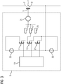
- FIG. 1 shows a circuit diagram of an IGBT 1 and a first embodiment of a gate driver 3 for an IGBT 1.
- the IGBT 1 has a gate 5, a collector 7 and an emitter 9.
- the gate driver 3 has a switch-on semiconductor switch 11, a switch-off semiconductor switch 13, a switch-on resistor 15, a switch-off resistor 17, a control logic 19, an optional current measuring device 21, a switch-on voltage source 23 and a switch-off voltage source 25.
- the switch-on semiconductor switch 11 is connected to the gate 5 of the IGBT 1 via the switch-on resistor 15.
- the switch-off semiconductor switch 13 is connected to the gate 5 of the IGBT 1 via the switch-off resistor 17.
- the switch-on semiconductor switch 11 and the switch-off semiconductor switch 13 can be controlled by the control logic 19.
- the switch-on semiconductor switch 11, the switch-on resistor 15, the switch-off semiconductor switch 13 and the switch-off resistor 17 form a half-bridge with a bridge branch which is connected to the gate 5 of the IGBT 1, a first bridge arm in which the switch-on semiconductor switch 11 and the switch-on resistor 15 are arranged, and a second bridge arm in which the switch-off semiconductor switch 13 and the switch-off resistor 17 are arranged.
- the current measuring device 21 is arranged in the bridge branch of the half-bridge.
- the switch-on voltage source 23 generates a switch-on supply voltage for the switch-on semiconductor switch 11.
- the switch-off voltage source 25 generates a switch-off supply voltage for the switch-off semiconductor switch 13.
- the switch-on semiconductor switch 11 and the switch-off semiconductor switch 13 are each designed as a metal-oxide-semiconductor field-effect transistor (MOSFET), more precisely as a normally blocking n-channel MOSFET, whose Gate connection is connected to the control logic 19.
- MOSFET metal-oxide-semiconductor field-effect transistor
- the source connection of the switch-on semiconductor switch 11 is connected to the switch-on resistor 15.
- the drain connection of the switch-off semiconductor switch 13 is connected to the switch-off resistor 17.
- a first pole of the switch-on voltage source 23 is connected to the drain connection of the switch-on semiconductor switch 11.
- a first pole of the switch-off voltage source 25 is connected to the source connection of the switch-off semiconductor switch 13.
- the second pole of the switch-on voltage source 23 and the second pole of the switch-off voltage source 25 are connected to one another and to the emitter 9 of the IGBT 1.
- the second poles of the switch-on voltage source 23 and the switch-off voltage source 25 are therefore at a common first electrical potential.
- the first pole of the switch-on voltage source 23 is at a second electrical potential that is higher than the first electrical potential.
- the first pole of the switch-off voltage source 25 is at a third electrical potential, which is lower than the first electrical potential.
- the switch-on supply voltage is therefore positive, the switch-off supply voltage is negative.
- FIG 2 illustrates the inventive method for operating an IGBT 1 with an in FIG. 1 shown gate driver 3 based on the course of a switching state S1 of the IGBT 1, one Switching state S2 of the switch-on semiconductor switch 11 and a switching state S3 of the switch-off semiconductor switch 13 as a function of a time t.
- Each switching state S1, S2, S3 alternately assumes the value one, which denotes an on state, and the value zero, which denotes an off state.
- a maximum stationary reverse voltage required for operation of the IGBT 1 a minimum removal charge, the removal of which at gate 5 of the IGBT 1 causes an electric field strength which enables the IGBT 1 to absorb the maximum stationary reverse voltage during stationary locking can, and a maximum removal charge, the removal of which causes an electric field strength at the gate 5, which leads to a dynamic avalanche.
- the IGBT 1 is switched on alternately for a switch-on duration T1 and switched off for a switch-off duration T2.
- the switch-on semiconductor switch 11 is switched on and the switch-off semiconductor switch 13 is switched off.
- the switch-on semiconductor switch 11 is switched off and the switch-off semiconductor switch 13 is first switched on for a charge removal period T3 and switched off after the charge removal period T3 has expired.
- the charge removal time T3 is defined by taking a predetermined removal charge, which is greater than the minimum removal charge and smaller than the maximum removal charge, from the gate 5 of the IGBT 1 during the charge removal time T3, that is to say the switch-off semiconductor switch 13 is switched off as soon as the Charge removed from the gate 5 reaches the removal charge.
- a current flowing in the gate is continuously detected with the current measuring device 21 and the charge removed from the gate is determined by means of the control logic 19 from the detected gate current by integrating the gate current over time after the switch-off semiconductor switch 13 has been switched on.
- turn off the semiconductor switch 13 between the gate 5 and the emitter 9 via the turn-off resistor 17 generates a turn-off voltage which generates a constant gate current
- the charge removal time T3 is defined by the quotient of the removal charge and the constant gate current.
- FIG 3 shows a circuit diagram of an IGBT 1 and a second embodiment of a gate driver 3 for an IGBT 1.
- the gate driver 3 differs from that in FIG. 1
- the exemplary embodiment shown is merely by means of a series connection of an additional switch-off semiconductor switch 27 and an additional switch-off resistor 29 connected in parallel to the switch-off semiconductor switch 13 and the switch-off resistor 17.
- the additional switch-off resistor 29 is larger than the switch-off resistor 17.
- the additional switch-off semiconductor switch 27 is designed as a normally blocking n-channel MOSFET.
- the gate connection of the additional switch-off semiconductor switch 27 is connected to the control logic 19, so that the additional switch-off semiconductor switch 27 can be controlled by the control logic 19.
- the drain connection of the additional switch-off semiconductor switch 27 is connected to the gate 5 of the IGBT 1 via the additional switch-off resistor 29.
- the source connection of the additional switch-off semiconductor switch 27 is connected to the first pole of the switch-off voltage source 25.
- FIG 4 illustrates the inventive method for operating an IGBT 1 with an in Figure 3 Gate driver 3 shown on the basis of time profiles of a switching state S1 of the IGBT 1, a switching state S2 of the switch-on semiconductor switch 11, a switching state S3 of the switch-off semiconductor switch 13 and a switching state S4 of the additional switch-off semiconductor switch 27.
- a maximum stationary reverse voltage required for operation of the IGBT 1 a minimum removal charge, the removal of which at the gate 5 of the IGBT 1 causes an electric field strength which enables the IGBT 1 to achieve the maximum stationary reverse voltage during stationary locking can record, and a maximum removal charge, the removal of which causes an electric field strength at the gate 5, which leads to a dynamic avalanche.
- the IGBT 1 is switched on alternately for a switch-on duration T1 and switched off for a switch-off duration T2.
- the switch-on semiconductor switch 11 is switched on and the switch-off semiconductor switch 13 and the additional switch-off semiconductor switch 27 are switched off.
- the switch-on semiconductor switch 11 is switched off, the switch-off semiconductor switch 13 is first switched on for a charge removal period T3 and is switched off after the charge withdrawal period T3 has expired, and the additional switch-off semiconductor switch 27 is switched on.
- the charge removal duration T3 is defined in that a removal charge which is greater than the minimum removal charge and less than the maximum removal charge is removed from the gate 5 of the IGBT 1 during a switch-off period T2.
- the described exemplary embodiment of the method according to the invention takes charge from the gate 5 by switching on the additional switch-off semiconductor switch 27 during the entire switch-off period T2. If the additional switch-off resistance 29 is sufficiently large, however, the charge withdrawn from the gate 5 after the switch-off semiconductor switch 13 has been switched off during the switch-off period T2, so that it can either be completely neglected, or the determination of the charge removal duration T3 is based on a maximum removal charge reduced by this charge placed.
- the switch-off behavior of the IGBT 1 can advantageously be stabilized.
- FIG 5 shows a circuit diagram of an IGBT 1 and a third embodiment of a gate driver 3 for an IGBT 1.
- the gate driver 3 differs from that in FIG. 1 illustrated embodiment in that instead of the series connection of the switch-off semiconductor switch 13 and Switch-off resistor 17 has a switch-off current source 31 for generating a constant gate current.
- the switch-off current source 31 is analogous to the switch-off semiconductor switch 13 in the on the basis of Figure 2
- the described embodiment of the method according to the invention is switched on during a switch-off period T2 of the IGBT 1 for a charge removal period T3.
- the charge removal time T3 is defined by the quotient of the removal charge and the constant gate current.
- the switch-off current source 31 is switched off.
- the switch-off current source 31 is realized by a series connection of a bipolar transistor 33 which can be controlled by the control logic 19 and a current source resistor 35.
- the control logic 19 controls the switch-off current source 31 to be controlled by the control logic 19.
- other designs of a switch-off current source 31 which can be controlled by the control logic 19 are also possible.
- FIG 6 shows a circuit diagram of a half-bridge circuit with two IGBT 1, 2, a first gate driver 3 for a first IGBT 1 and a second gate driver 4 for the second IGBT 2.
- Each IGBT 1, 2 is arranged in a bridge arm of a half-bridge. The bridge arms are connected to one another by a capacitor 37.
- a free-wheeling diode 39, 40 is connected in parallel to each IGBT 1, 2.
- Each gate driver 3, 4 is like the gate driver 3 of the in FIG. 1 or FIG 5 illustrated embodiment trained.
- FIG 7 illustrates the inventive method for operating two according to FIG 6 to a half-bridge connected IGBT 1, 2 on the basis of time profiles of a switching state S1 of the first IGBT 1, a switching state S2 of the switch-on semiconductor switch 11 of the first gate driver 3, a switching state S3 of the switch-off semiconductor switch 13 of the first gate driver 3, a switching state S5 of second IGBT 2, a switching state S6 of the switch-on semiconductor switch 11 of the second gate driver 4 and a switching state S7 of the switch-off semiconductor switch 13 of the second gate driver 4.
- the two IGBTs 1, 2 are switched on alternately for a duty cycle T1, two successive duty cycles T1 being separated from one another by a locking period T4 in which both IGBTs 1, 2 are switched off.
- the gate 5 of the IGBT 1, 2 is analogous to that based on FIG Figure 2 described method removed a removal load that is greater than the minimum removal load intended for him and smaller than the maximum removal load determined for him.
- the charge removal time T3 is divided into two charge removal time parts T31, T32 separated by a removal pause T5, a first charge removal time part T31 starting with the switching off of the IGBT 1, 2 and ending before the other IGBT 2, 1 is switched on, and the second charge removal time part T32 after the end of the first charge removal period T31 and before the other IGBT 2, 1 is switched on and ends with the switching on of the IGBT 1, 2.
Landscapes
- Power Conversion In General (AREA)
- Electronic Switches (AREA)
Abstract
Die Erfindung betrifft ein Verfahren zum Betreiben eines IGBT (1, 2), wobei eine für einen Betrieb des IGBT (1, 2) erforderliche maximale stationäre Sperrspannung bestimmt wird, eine minimale Entnahmeladung bestimmt wird, deren Entnahme am Gate (5) des IGBT (1, 2) eine elektrische Feldstärke bewirkt, die es ermöglicht, dass der IGBT (1, 2) beim stationären Sperren die maximale stationäre Sperrspannung aufnehmen kann, eine maximale Entnahmeladung bestimmt wird, deren Entnahme am Gate (5) eine elektrische Feldstärke bewirkt, die zu einem dynamischen Avalanche führt, und dem Gate (5) beim Ausschalten des IGBT (1, 2) während einer Ladungsentnahmedauer (T3) eine Entnahmeladung entnommen wird, die größer als die minimale Entnahmeladung und kleiner als die maximale Entnahmeladung ist.The invention relates to a method for operating an IGBT (1, 2), wherein a maximum stationary reverse voltage required for operation of the IGBT (1, 2) is determined, a minimum removal charge is determined, the removal of which at the gate (5) of the IGBT ( 1, 2) causes an electrical field strength that enables the IGBT (1, 2) to absorb the maximum stationary blocking voltage during stationary blocking, a maximum removal charge is determined, the removal of which at the gate (5) causes an electrical field strength that leads to a dynamic avalanche, and a removal charge which is greater than the minimum removal charge and smaller than the maximum removal charge is removed from the gate (5) when the IGBT (1, 2) is switched off during a charge removal period (T3).
Description
Die Erfindung betrifft ein Verfahren und einen Gate-Treiber zum Betreiben eines Bipolartransistors mit isolierter Gate-Elektrode (IGBT, englisch: insulated-gate bipolar transistor) .The invention relates to a method and a gate driver for operating a bipolar transistor with an insulated gate electrode (IGBT, English: insulated-gate bipolar transistor).
Bei dem Ausschalten eines IGBT treten in dem IGBT hohe elektrische Feldstärken auf, die zu dynamischem Avalance führen können. Dies kann zum spontanen Ausfall oder zu einer langfristigen Degeneration des IGBT führen. Besonders ausgeprägt ist dieses Problem bei hohen Sperrspannungen im Bereich von 3,3 kV und darüber. Im bekannten Stand der Technik wird das Problem beispielsweise dadurch gelöst, dass die Schaltgeschwindigkeit des IGBT reduziert wird. Die Reduktion der Schaltgeschwindigkeit reduziert die Feldstärkebelastung des IGBT und kann daher dynamischen Avalance verhindern. Allerdings vergrößert eine Reduktion der Schaltgeschwindigkeit die Ausschaltverluste beim Ausschalten des IGBT.When an IGBT is switched off, high electrical field strengths occur in the IGBT, which can lead to dynamic avalance. This can lead to spontaneous failure or long-term degeneration of the IGBT. This problem is particularly pronounced at high reverse voltages in the range of 3.3 kV and above. In the known prior art, the problem is solved, for example, by reducing the switching speed of the IGBT. The reduction of the switching speed reduces the field strength load of the IGBT and can therefore prevent dynamic avalance. However, a reduction in the switching speed increases the switch-off losses when the IGBT is switched off.
Der Erfindung liegt die Aufgabe zugrunde, dynamischen Avalance beim Ausschalten eines IGBT zu verhindern, ohne dabei die Schaltgeschwindigkeit des IGBT im Normalbetrieb zu reduzieren.The invention has for its object to prevent dynamic avalance when switching off an IGBT without reducing the switching speed of the IGBT in normal operation.
Die Aufgabe wird erfindungsgemäß durch ein Verfahren mit den Merkmalen des Anspruchs 1 und einen Gate-Treiber mit den Merkmalen des Anspruchs 8 gelöst.The object is achieved according to the invention by a method with the features of
Vorteilhafte Ausgestaltungen der Erfindung sind Gegenstand der abhängigen Ansprüche.Advantageous embodiments of the invention are the subject of the dependent claims.
Bei dem erfindungsgemäßen Verfahren zum Betreiben eines IGBT werden zunächst eine für einen Betrieb des IGBT erforderliche maximale stationäre Sperrspannung, eine minimale Entnahmeladung, deren Entnahme am Gate des IGBT eine elektrische Feldstärke bewirkt, die es ermöglicht, dass der IGBT beim stationären Sperren die maximale stationäre Sperrspannung aufnehmen kann, und eine maximale Entnahmeladung, deren Entnahme am Gate eine elektrische Feldstärke bewirkt, die zu einem dynamischen Avalanche führt, bestimmt. Dem Gate wird beim Ausschalten des IGBT während einer Ladungsentnahmedauer eine Entnahmeladung entnommen, die größer als die minimale Entnahmeladung und kleiner als die maximale Entnahmeladung ist.In the method according to the invention for operating an IGBT, first of all a maximum stationary reverse voltage required for operating the IGBT, a minimum removal charge, their removal at the gate of the IGBT causes an electric field strength that enables the IGBT to absorb the maximum stationary reverse voltage during stationary blocking, and determines a maximum removal charge, the removal of which at the gate causes an electric field strength that leads to a dynamic avalanche . When the IGBT is switched off, a removal charge which is greater than the minimum removal charge and smaller than the maximum removal charge is removed during a charge removal period.
Die Erfindung sieht vor, beim Ausschalten des IGBT eine Ladungsmenge zu steuern, die dem Gate des IGBT entnommen wird, um dynamischen Avalanche zu verhindern. Die Erfindung nutzt aus, dass die beim Ausschalten in dem IGBT auftretenden elektrischen Feldstärken von der Ladung abhängen, die dem Gate des IGBT beim Ausschalten entnommen wird. Die der Erfindung zugrunde liegende Idee ist, die dem Gate beim Ausschalten entnommene Ladungsmenge zu begrenzen, um dynamischen Avalanche zu verhindern. Dazu werden eine minimale Entnahmeladung, deren Entnahme am Gate die Aufnahme einer maximalen stationären Sperrspannung durch den IGBT ermöglicht, und eine maximale Entnahmeladung, deren Entnahme am Gate zu einem dynamischen Avalanche führt, bestimmt und dem Gate wird beim Ausschalten des IGBT eine Entnahmeladung entnommen, die zwischen der minimalen und der maximalen Entnahmeladung liegt. Dadurch wird beim Ausschalten des IGBT dynamischer Avalanche verhindert, ohne die Schaltgeschwindigkeit des IGBT im Nennbetrieb reduzieren zu müssen und dadurch die Ausschaltverluste beim Ausschalten des IGBT im Nennbetrieb zu erhöhen.The invention provides for a quantity of charge to be controlled when the IGBT is switched off and which is removed from the gate of the IGBT in order to prevent dynamic avalanche. The invention takes advantage of the fact that the electric field strengths that occur in the IGBT when it is switched off depend on the charge that is taken from the gate of the IGBT when it is turned off. The idea on which the invention is based is to limit the amount of charge removed from the gate when it is switched off in order to prevent dynamic avalanche. For this purpose, a minimum removal charge, the removal of which at the gate enables a maximum stationary reverse voltage to be picked up by the IGBT, and a maximum removal charge, the removal of which at the gate leads to a dynamic avalanche, and a removal charge which is removed from the gate when the IGBT is switched off lies between the minimum and the maximum removal load. This prevents dynamic avalanche when switching off the IGBT without having to reduce the switching speed of the IGBT in nominal operation and thereby increasing the switch-off losses when switching off the IGBT in nominal operation.
Bei einer Ausgestaltung der Erfindung wird die Entnahmeladung durch Anlegen einer Ausschaltspannung zwischen dem Gate und dem Emitter während der Ladungsentnahmedauer entnommen. Beispielsweise wird ferner während des Anlegens der Ausschaltspannung ein in dem Gate fließender Gatestrom gemessen, aus dem Gatestrom wird eine dem Gate entnommene Ladung ermittelt und ein Ende der Ladungsentnahmedauer wird dadurch definiert, dass die dem Gate entnommene Ladung die Entnahmeladung erreicht. Diese Ausgestaltung der Erfindung sieht also vor, die dem Gate beim Ausschalten des IGBT entnommene Ladung durch das Anlegen einer Gate-Emitter-Spannung während der Ladungsentnahmedauer zu steuern. Das Messen der dem Gate entnommenen Ladung ermöglicht die Begrenzung dieser Ladung auf die Entnahmeladung insbesondere auch dann, wenn der Gatestrom in dem Gate während der Ladungsentnahmedauer nicht konstant ist.In one embodiment of the invention, the removal charge is removed by applying a switch-off voltage between the gate and the emitter during the charge removal period. For example, a gate current flowing in the gate is also measured during the application of the switch-off voltage, a charge removed from the gate is determined from the gate current, and an end of the charge removal period is defined in that the charge removed from the gate reaches the removal charge. This embodiment of the invention therefore provides for the charge removed from the gate when the IGBT is switched off to be controlled by applying a gate-emitter voltage during the charge removal period. The measurement of the charge removed from the gate enables this charge to be limited to the removal charge, particularly when the gate current in the gate is not constant during the charge removal period.
Bei einer weiteren Ausgestaltung der Erfindung wird die Entnahmeladung durch Erzeugen eines während der Ladungsentnahmedauer in dem Gate fließenden konstanten Gatestroms entnommen. Diese Ausgestaltung der Erfindung ermöglicht die Definition der Ladungsentnahmedauer als den Quotienten der Entnahmeladung und des konstanten Gatestroms. Wenn der Gatestrom bekannt ist, wird dazu keine Messung des Gatestroms benötigt.In a further embodiment of the invention, the removal charge is removed by generating a constant gate current flowing in the gate during the charge removal period. This embodiment of the invention enables the charge removal time to be defined as the quotient of the removal charge and the constant gate current. If the gate current is known, no measurement of the gate current is required.
Bei einer weiteren Ausgestaltung der Erfindung wird ein Schwellenwert für die Gate-Emitter-Spannung des IGBT vorgegeben und die Entnahme von Ladung aus dem Gate wird abgebrochen, wenn die Gate-Emitter-Spannung den Schwellenwert erreicht. Diese Ausgestaltung der Erfindung verhindert, dass die Gate-Emitter-Spannung beim Ausschalten des IGBT zu niedrig wird und zu einer Beschädigung des IGBT führt.In a further embodiment of the invention, a threshold value for the gate-emitter voltage of the IGBT is specified and the removal of charge from the gate is interrupted when the gate-emitter voltage reaches the threshold value. This embodiment of the invention prevents the gate-emitter voltage from becoming too low when the IGBT is switched off and leading to damage to the IGBT.
Bei dem erfindungsgemäßen Verfahren zum Betreiben zweier zu einer Halbbrücke verschalteter IGBT wird jeder IGBT mit dem oben beschriebenen erfindungsgemäßen Verfahren oder einer seiner Ausgestaltungen betrieben. Die beiden IGBT werden abwechselnd für jeweils eine Einschaltdauer eingeschaltet, wobei je zwei aufeinander folgende Einschaltdauern durch eine Verriegelungsdauer, in der beide IGBT ausgeschaltet sind, voneinander getrennt sind. Die Ladungsentnahmedauer für jeden IGBT wird in zwei durch eine Entnahmepause voneinander getrennte Ladungsentnahmedauerteile aufgeteilt, wobei ein erster Ladungsentnahmedauerteil mit dem Ausschalten des IGBT beginnt und vor dem Einschalten des anderen IGBT endet und der zweite Ladungsentnahmedauerteil nach dem Ende des ersten Ladungsentnahmedauerteils und vor dem Einschalten des anderen IGBT beginnt und mit dem Einschalten des IGBT endet.In the method according to the invention for operating two IGBTs connected to form a half-bridge, each IGBT is operated using the method according to the invention described above or one of its refinements. The two IGBTs are switched on alternately for a duty cycle, two successive duty cycles being separated from one another by a locking period in which both IGBTs are switched off. The charge withdrawal period for each IGBT is divided into two charge withdrawal periods separated by a withdrawal pause, with a first charge withdrawal period beginning when the IGBT is switched off and ending before the other IGBT is switched on, and the second charge withdrawal period after the end of the first charge withdrawal period and starts before the other IGBT is switched on and ends with the switching on of the IGBT.
Das vorgenannte Verfahren berücksichtigt, dass es je nach dem Verhältnis zwischen der Millerkapazität und der Gate-Emitter-Kapazität in einem IGBT und der negativen treibenden Spannung der Ansteuerschaltung bei Anwendung des erfindungsgemäßen Verfahrens bei dem Ausschalten des IGBT dazu kommen kann, dass die Gate-Emitter-Spannung bereits die negative treibende Spannung erreicht hat, bevor die vorgesehene Entnahmeladung dem Gate entnommen werden konnte. Beim Einschalten des anderen IGBT nimmt der ausgeschaltete IGBT dann Spannung auf. Durch die Millerkapazität kann es daraufhin zu einem parasitären Einschalten des hochohmig angesteuerten, ausgeschalteten IGBT kommen. Bei dem vorgenannten Verfahren wird dies dadurch vermieden, dass die Ladungsentnahme aus dem Gate unterbrochen wird und nach der Unterbrechung vor dem Ablauf der Verriegelungszeit, aber nach dem Ablauf eines regulären Ausschaltvorgangs wieder aufgenommen wird und das Gate auf diese Weise auf niedrigem Potential unterhalb der Thresholdspannung des IGBT gehalten wird.The aforementioned method takes into account that, depending on the ratio between the miller capacitance and the gate-emitter capacitance in an IGBT and the negative driving voltage of the drive circuit when the method according to the invention is used when the IGBT is switched off, the gate-emitters can occur Voltage has already reached the negative driving voltage before the intended removal charge could be removed from the gate. When the other IGBT is switched on, the switched off IGBT then takes up voltage. The miller capacitance can then result in a parasitic switching on of the high-resistance controlled, switched-off IGBT. In the aforementioned method, this is avoided by interrupting the charge removal from the gate and resuming it after the interruption before the expiry of the locking time, but after the end of a regular switch-off process, and in this way the gate at a low potential below the threshold voltage of the IGBT is held.
Bei den vorgenannten erfindungsgemäßen Verfahren und deren Ausgestaltungen beträgt die Ladungsentnahmedauer beispielsweise zwischen einhundert Nanosekunden und zehn Mikrosekunden. Eine derartige Ladungsentnahmedauer ermöglicht in der Regel das Entnehmen einer Ladung aus dem Gate eines IGBT, die zwischen der minimalen und der maximalen Entnahmeladung liegt.In the aforementioned methods according to the invention and their configurations, the charge removal time is, for example, between one hundred nanoseconds and ten microseconds. Such a charge removal period generally enables a charge to be withdrawn from the gate of an IGBT that lies between the minimum and the maximum removal charge.
Ein erfindungsgemäßer Gate-Treiber für einen IGBT zur Durchführung des erfindungsgemäßen Verfahrens ist dazu ausgebildet, den IGBT abwechselnd für eine Einschaltdauer einzuschalten und für eine Ausschaltdauer auszuschalten und dem Gate des IGBT in jeder Ausschaltdauer die Entnahmeladung zu entnehmen.A gate driver according to the invention for an IGBT for carrying out the method according to the invention is designed to switch on the IGBT alternately for a switch-on period and switch it off for a switch-off period and to remove the removal charge from the gate of the IGBT in each switch-off period.
Eine Ausgestaltung des erfindungsgemäßen Gate-Treibers sieht einen ansteuerbaren Ausschalthalbleiterschalter, der zum Anlegen einer Ausschaltspannung zwischen dem Gate und dem Emitter des IGBT einschaltbar ist, einen zwischen den Ausschalthalbleiterschalter und das Gate geschalteten oder der Gate-Emitter-Strecke des IGBT nachgeschalteten Ausschaltwiderstand und eine Ansteuerlogik, die dazu ausgebildet ist, den Ausschalthalbleiterschalter für die Ladungsentnahmedauer einzuschalten, vor. Der Gate-Treiber kann ferner eine Strommessvorrichtung zum Messen eines in dem Gate fließenden Gatestroms aufweisen, wobei die Ansteuerlogik dazu ausgebildet ist, aus dem Gatestrom eine dem Gate entnommene Ladung zu ermitteln und ein Ende der Ladungsentnahmedauer dadurch zu definieren, dass die dem Gate entnommene Ladung die Entnahmeladung erreicht. Alternativ oder zusätzlich kann der Gate-Treiber eine zu dem Ausschalthalbleiterschalter und dem Ausschaltwiderstand parallel geschaltete Reihenschaltung eines Zusatzausschalthalbleiterschalters und eines Zusatzausschaltwiderstands aufweisen, wobei der Zusatzausschaltwiderstand größer als der Ausschaltwiderstand ist und der Zusatzausschalthalbleiterschalter zum Anlegen einer Zusatzausschaltspannung zwischen dem Gate und dem Emitter einschaltbar ist.An embodiment of the gate driver according to the invention provides a controllable switch-off semiconductor switch which can be switched on to apply a switch-off voltage between the gate and the emitter of the IGBT, a switch-off resistor connected between the switch-off semiconductor switch and the gate or connected downstream of the gate-emitter path of the IGBT and a control logic , which is designed to switch on the switch-off semiconductor switch for the charge removal period. The gate driver can furthermore have a current measuring device for measuring a gate current flowing in the gate, the drive logic being designed to determine a charge removed from the gate current from the gate current and to define an end of the charge removal period in that the charge removed from the gate reached the removal load. Alternatively or additionally, the gate driver can have a series connection of an additional switch-off semiconductor switch and an additional switch-off resistor connected in parallel with the switch-off semiconductor switch and the switch-off resistor, the additional switch-off resistance being greater than the switch-off resistance and the additional switch-off semiconductor switch being switchable for applying an additional switch-off voltage between the gate and the emitter.
Die vorgenannten Ausgestaltungen des erfindungsgemäßen Gate-Treibers ermöglichen die Ladungsentnahme aus dem Gate eines IGBT mittels eines Ausschalthalbleiterschalters und Ausschaltwiderstands sowie einer Ansteuerlogik zum Ansteuern des Ausschalthalbleiterschalters, um den Ausschalthalbleiterschalter für die Ladungsentnahme aus dem Gate einzuschalten und zum Beenden der Ladungsentnahme auszuschalten. Eine den Gatestrom messende Strommessvorrichtung ermöglicht die Bestimmung der dem Gate entnommenen Ladung durch Integration des Gatestroms über die Zeit und damit die Begrenzung der Ladungsentnahme auf die vorgesehene Entnahmeladung durch ein Beenden der Ladungsentnahme beim Erreichen der Entnahmeladung. Durch eine parallel zu dem Ausschalthalbleiterschalter und dem Ausschaltwiderstand geschaltete Reihenschaltung eines Zusatzausschalthalbleiterschalters und eines Zusatzausschaltwiderstands, der größer als der Ausschaltwiderstand ist, kann das Ausschaltverhalten des IGBT vorteilhaft stabilisiert werden, indem der Zusatzausschalthalbleiterschalter während der Ausschaltdauer des IGBT eingeschaltet wird. Durch die Wahl eines ausreichend großen Zusatzausschaltwiderstands kann dabei erreicht werden, dass dem Gate des IGBT durch das Einschalten des Zusatzausschalthalbleiterschalters nur wenig zusätzliche Ladung entnommen wird, so dass dem Gate die Entnahmeladung überwiegend durch das Einschalten des Ausschalthalbleiterschalters entnommen wird.The aforementioned embodiments of the gate driver according to the invention enable charge removal from the gate of an IGBT by means of a switch-off semiconductor switch and switch-off resistor, as well as a control logic for controlling the switch-off semiconductor switch, in order to switch on the switch-off semiconductor switch for removing charge from the gate and to switch it off when the charge is removed. A current measuring device measuring the gate current enables the charge removed from the gate to be determined by integrating the gate current over time and thus limiting the charge removal to the intended removal charge by terminating the charge removal when the removal charge is reached. Through a series connection of an additional switch-off semiconductor switch and an additional switch-off resistor connected in parallel with the switch-off semiconductor switch and the switch-off resistor, which is greater than the switch-off resistance, the switch-off behavior of the IGBT can advantageously be stabilized by switching on the additional switch-off semiconductor switch during the switch-off period of the IGBT. By choosing a sufficiently large additional switch-off resistance, it can be achieved that only a little additional charge is removed from the gate of the IGBT by switching on the additional switch-off semiconductor switch, so that the removal charge is withdrawn from the gate predominantly by switching on the switch-off semiconductor switch.
Eine weitere Ausgestaltung des erfindungsgemäßen Gate-Treibers sieht eine ansteuerbare Ausschaltstromquelle, die zum Erzeugen eines konstanten Gatestroms in dem Gate einschaltbar ist, und eine Ansteuerlogik, die dazu ausgebildet ist, die Ausschaltstromquelle für die Ladungsentnahmedauer einzuschalten, vor. Diese Ausgestaltung des erfindungsgemäßen Gate-Treibers ermöglicht eine Definition der Ladungsentnahmedauer durch den Quotienten aus der Entnahmeladung und dem konstanten Gatestrom, so dass bei einem bekannten konstanten Gatestrom insbesondere keine Strommessvorrichtung zum Messen des Gatestroms erforderlich ist.Another embodiment of the gate driver according to the invention provides a controllable switch-off current source that can be switched on to generate a constant gate current in the gate, and a control logic that is designed to switch on the switch-off current source for the charge removal duration. This configuration of the gate driver according to the invention enables the charge removal duration to be defined by the quotient of the removal charge and the constant gate current, so that, in particular, with a known constant gate current no current measuring device is required to measure the gate current.
Die oben beschriebenen Eigenschaften, Merkmale und Vorteile dieser Erfindung sowie die Art und Weise, wie diese erreicht werden, werden klarer und deutlicher verständlich im Zusammenhang mit der folgenden Beschreibung von Ausführungsbeispielen, die im Zusammenhang mit den Zeichnungen näher erläutert werden. Dabei zeigen:
- FIG 1
- einen Schaltplan eines IGBT und eines ersten Ausführungsbeispiels eines Gate-Treibers für einen IGBT,
- FIG 2
- zeitliche Verläufe von Schaltzuständen des IGBT und des Gate-Treibers, die in
Figur 1 - FIG 3
- einen Schaltplan eines IGBT und eines zweiten Ausführungsbeispiels eines Gate-Treibers für einen IGBT,
- FIG 4
- zeitliche Verläufe von Schaltzuständen des IGBT und des Gate-Treibers, die in
FIG 3 gezeigt sind, - FIG 5
- einen Schaltplan eines IGBT und eines dritten Ausführungsbeispiels eines Gate-Treibers für einen IGBT,
- FIG 6
- einen Schaltplan einer Halbbrückenschaltung mit zwei IGBT und einem Gate-Treiber für jeden IGBT,
- FIG 7
- zeitliche Verläufe von Schaltzuständen der IGBT und Gate-Treiber, die in
FIG 6 gezeigt sind.
- FIG. 1
- 1 shows a circuit diagram of an IGBT and a first exemplary embodiment of a gate driver for an IGBT,
- FIG 2
- temporal courses of switching states of the IGBT and the gate driver, which in
Figure 1 are shown - FIG 3
- 1 shows a circuit diagram of an IGBT and a second exemplary embodiment of a gate driver for an IGBT,
- FIG 4
- temporal courses of switching states of the IGBT and the gate driver, which in
FIG 3 are shown - FIG 5
- 1 shows a circuit diagram of an IGBT and a third exemplary embodiment of a gate driver for an IGBT,
- FIG 6
- a circuit diagram of a half-bridge circuit with two IGBT and a gate driver for each IGBT,
- FIG 7
- temporal courses of switching states of the IGBT and gate drivers that are in
FIG 6 are shown.
Einander entsprechende Teile sind in den Figuren mit denselben Bezugszeichen versehen.Corresponding parts are provided with the same reference symbols in the figures.
Der IGBT 1 weist ein Gate 5, einen Kollektor 7 und einen Emitter 9 auf.The
Der Gate-Treiber 3 weist einen Einschalthalbleiterschalter 11, einen Ausschalthalbleiterschalter 13, einen Einschaltwiderstand 15, einen Ausschaltwiderstand 17, eine Ansteuerlogik 19, eine optionale Strommessvorrichtung 21, eine Einschaltspannungsquelle 23 und eine Ausschaltspannungsquelle 25 auf.The gate driver 3 has a switch-on semiconductor switch 11, a switch-off
Der Einschalthalbleiterschalter 11 ist über den Einschaltwiderstand 15 mit dem Gate 5 des IGBT 1 verbunden. Der Ausschalthalbleiterschalter 13 ist über den Ausschaltwiderstand 17 mit dem Gate 5 des IGBT 1 verbunden. Der Einschalthalbleiterschalter 11 und der Ausschalthalbleiterschalter 13 sind von der Ansteuerlogik 19 ansteuerbar. Der Einschalthalbleiterschalter 11, der Einschaltwiderstand 15, der Ausschalthalbleiterschalter 13 und der Ausschaltwiderstand 17 sind zu einer Halbbrücke mit einem Brückenzweig, der mit dem Gate 5 des IGBT 1 verbunden ist, einem ersten Brückenarm, in dem der Einschalthalbleiterschalter 11 und der Einschaltwiderstand 15 angeordnet sind, und einem zweiten Brückenarm, in dem der Ausschalthalbleiterschalter 13 und der Ausschaltwiderstand 17 angeordnet sind, verschaltet. Die Strommessvorrichtung 21 ist in dem Brückenzweig der Halbbrücke angeordnet.The switch-on semiconductor switch 11 is connected to the gate 5 of the
Die Einschaltspannungsquelle 23 erzeugt eine Einschaltversorgungsspannung für den Einschalthalbleiterschalter 11. Die Ausschaltspannungsquelle 25 erzeugt eine Ausschaltversorgungsspannung für den Ausschalthalbleiterschalter 13.The switch-on
In dem in
Bei dem Verfahren werden zunächst eine für einen Betrieb des IGBT 1 erforderliche maximale stationäre Sperrspannung, eine minimale Entnahmeladung, deren Entnahme am Gate 5 des IGBT 1 eine elektrische Feldstärke bewirkt, die es ermöglicht, dass der IGBT 1 beim stationären Sperren die maximale stationäre Sperrspannung aufnehmen kann, und eine maximale Entnahmeladung, deren Entnahme am Gate 5 eine elektrische Feldstärke bewirkt, die zu einem dynamischen Avalanche führt, bestimmt.In the method, a maximum stationary reverse voltage required for operation of the
Der IGBT 1 wird abwechselnd für eine Einschaltdauer T1 eingeschaltet und für eine Ausschaltdauer T2 ausgeschaltet. Während jeder Einschaltdauer T1 wird der Einschalthalbleiterschalter 11 eingeschaltet und der Ausschalthalbleiterschalter 13 wird ausgeschaltet. Während jeder Ausschaltdauer T2 wird der Einschalthalbleiterschalter 11 ausgeschaltet und der Ausschalthalbleiterschalter 13 wird zunächst für eine Ladungsentnahmedauer T3 eingeschaltet und nach dem Ablauf der Ladungsentnahmedauer T3 ausgeschaltet. Die Ladungsentnahmedauer T3 wird dadurch definiert, dass dem Gate 5 des IGBT 1 während der Ladungsentnahmedauer T3 eine vorher bestimmte Entnahmeladung, die größer als die minimale Entnahmeladung und kleiner als die maximale Entnahmeladung ist, entnommen wird, das heißt der Ausschalthalbleiterschalter 13 wird ausgeschaltet, sobald die dem Gate 5 entnommene Ladung die Entnahmeladung erreicht. Dazu wird beispielsweise mit der Strommessvorrichtung 21 laufend ein in dem Gate fließender Gatestrom erfasst und mittels der Ansteuerlogik 19 aus dem erfassten Gatestrom die dem Gate entnommene Ladung ermittelt, indem der Gatestrom nach dem Einschalten des Ausschalthalbleiterschalters 13 über die Zeit integriert wird. Alternativ wird mit dem Ausschalthalbleiterschalter 13 zwischen dem Gate 5 und dem Emitter 9 über den Ausschaltwiderstand 17 eine Ausschaltspannung erzeugt, die einen konstanten Gatestrom erzeugt, und die Ladungsentnahmedauer T3 durch den Quotienten aus der Entnahmeladung und dem konstanten Gatestrom definiert.The
Wiederum werden eine für einen Betrieb des IGBT 1 erforderliche maximale stationäre Sperrspannung, eine minimale Entnahmeladung, deren Entnahme am Gate 5 des IGBT 1 eine elektrische Feldstärke bewirkt, die es ermöglicht, dass der IGBT 1 beim stationären Sperren die maximale stationäre Sperrspannung aufnehmen kann, und eine maximale Entnahmeladung, deren Entnahme am Gate 5 eine elektrische Feldstärke bewirkt, die zu einem dynamischen Avalanche führt, bestimmt.In turn, a maximum stationary reverse voltage required for operation of the
Der IGBT 1 wird abwechselnd für eine Einschaltdauer T1 eingeschaltet und für eine Ausschaltdauer T2 ausgeschaltet. Während jeder Einschaltdauer T1 wird der Einschalthalbleiterschalter 11 eingeschaltet und der Ausschalthalbleiterschalter 13 und der Zusatzausschalthalbleiterschalter 27 werden ausgeschaltet. Während jeder Ausschaltdauer T2 wird der Einschalthalbleiterschalter 11 ausgeschaltet, der Ausschalthalbleiterschalter 13 wird zunächst für eine Ladungsentnahmedauer T3 eingeschaltet und nach dem Ablauf der Ladungsentnahmedauer T3 ausgeschaltet und der Zusatzausschalthalbleiterschalter 27 wird eingeschaltet. Die Ladungsentnahmedauer T3 wird dadurch definiert, dass dem Gate 5 des IGBT 1 während einer Ausschaltdauer T2 eine Entnahmeladung, die größer als die minimale Entnahmeladung und kleiner als die maximale Entnahmeladung ist, entnommen wird. Im Unterschied zu dem anhand von
Für jeden IGBT 1, 2 wird eine für dessen Betrieb erforderliche maximale stationäre Sperrspannung, eine minimale Entnahmeladung, deren Entnahme am Gate 5 des IGBT 1, 2 eine elektrische Feldstärke bewirkt, die es ermöglicht, dass der IGBT 1 beim stationären Sperren die maximale stationäre Sperrspannung aufnehmen kann, und eine maximale Entnahmeladung, deren Entnahme am Gate 5 eine elektrische Feldstärke bewirkt, die zu einem dynamischen Avalanche führt, bestimmt.For each
Die beiden IGBT 1, 2 werden abwechselnd für jeweils eine Einschaltdauer T1 eingeschaltet, wobei je zwei aufeinander folgende Einschaltdauern T1 durch eine Verriegelungsdauer T4 voneinander getrennt sind, in der beide IGBT 1, 2 ausgeschaltet sind.The two
Während jeder Ausschaltdauer T2 jedes IGBT 1, 2 wird dem Gate 5 des IGBT 1, 2 während einer Ladungsentnahmedauer T3 analog zu dem anhand von
Das anhand von
Obwohl die Erfindung im Detail durch bevorzugte Ausführungsbeispiele näher illustriert und beschrieben wurde, so ist die Erfindung nicht durch die offenbarten Beispiele eingeschränkt und andere Variationen können vom Fachmann hieraus abgeleitet werden, ohne den Schutzumfang der Erfindung zu verlassen.Although the invention has been illustrated and described in detail by preferred exemplary embodiments, the invention is not restricted by the disclosed examples and other variations can be derived therefrom by a person skilled in the art without departing from the scope of protection of the invention.
Claims (12)
Priority Applications (5)
| Application Number | Priority Date | Filing Date | Title |
|---|---|---|---|
| EP18191128.0A EP3618278A1 (en) | 2018-08-28 | 2018-08-28 | Driving of a bipolar transistor having insulated gate electrode |
| US17/272,118 US11211923B2 (en) | 2018-08-28 | 2019-08-20 | Operating a bipolar transistor having an insulated gate electrode |
| CN201980057092.8A CN112640307B (en) | 2018-08-28 | 2019-08-20 | Method for operating an IGBT and gate driver |
| PCT/EP2019/072200 WO2020043540A1 (en) | 2018-08-28 | 2019-08-20 | Operating a bipolar transistor having an insulated gate electrode |
| EP19766181.2A EP3804136B1 (en) | 2018-08-28 | 2019-08-20 | Driving of a bipolar transistor having insulated gate electrode |
Applications Claiming Priority (1)
| Application Number | Priority Date | Filing Date | Title |
|---|---|---|---|
| EP18191128.0A EP3618278A1 (en) | 2018-08-28 | 2018-08-28 | Driving of a bipolar transistor having insulated gate electrode |
Publications (1)
| Publication Number | Publication Date |
|---|---|
| EP3618278A1 true EP3618278A1 (en) | 2020-03-04 |
Family
ID=63442446
Family Applications (2)
| Application Number | Title | Priority Date | Filing Date |
|---|---|---|---|
| EP18191128.0A Withdrawn EP3618278A1 (en) | 2018-08-28 | 2018-08-28 | Driving of a bipolar transistor having insulated gate electrode |
| EP19766181.2A Active EP3804136B1 (en) | 2018-08-28 | 2019-08-20 | Driving of a bipolar transistor having insulated gate electrode |
Family Applications After (1)
| Application Number | Title | Priority Date | Filing Date |
|---|---|---|---|
| EP19766181.2A Active EP3804136B1 (en) | 2018-08-28 | 2019-08-20 | Driving of a bipolar transistor having insulated gate electrode |
Country Status (4)
| Country | Link |
|---|---|
| US (1) | US11211923B2 (en) |
| EP (2) | EP3618278A1 (en) |
| CN (1) | CN112640307B (en) |
| WO (1) | WO2020043540A1 (en) |
Citations (2)
| Publication number | Priority date | Publication date | Assignee | Title |
|---|---|---|---|---|
| JP2002153043A (en) * | 2000-11-14 | 2002-05-24 | Fuji Electric Co Ltd | Gate drive device for voltage driven semiconductor device |
| DE102013223135B3 (en) * | 2013-11-13 | 2014-11-20 | Infineon Technologies Ag | Control circuit for power semiconductor switch |
Family Cites Families (14)
| Publication number | Priority date | Publication date | Assignee | Title |
|---|---|---|---|---|
| JP4144541B2 (en) * | 2004-03-19 | 2008-09-03 | 日産自動車株式会社 | Driver circuit for voltage-driven semiconductor device |
| JP5138287B2 (en) * | 2007-06-27 | 2013-02-06 | 三菱電機株式会社 | Gate drive device |
| JP5056955B2 (en) * | 2010-07-30 | 2012-10-24 | トヨタ自動車株式会社 | Driving device for driving voltage-driven element |
| WO2012146992A1 (en) * | 2011-04-28 | 2012-11-01 | Koninklijke Philips Electronics N.V. | Digitally controlled high speed high voltage gate driver circuit |
| CN102893525B (en) * | 2011-05-19 | 2013-12-25 | 丰田自动车株式会社 | Drive device for driving voltage-driven element |
| DE102012207147B4 (en) * | 2012-04-27 | 2016-01-21 | Infineon Technologies Ag | Method for driving power semiconductor switches |
| DE102013015723B3 (en) * | 2013-09-20 | 2014-09-04 | Hochschule Reutlingen | Improved control of power semiconductors |
| JP6362996B2 (en) * | 2014-10-24 | 2018-07-25 | 株式会社日立製作所 | Semiconductor drive device and power conversion device using the same |
| EP3012977A1 (en) * | 2014-10-24 | 2016-04-27 | ABB Technology AG | Method for switching a semiconductor module, semiconductor module and half-bridge |
| JP6402591B2 (en) * | 2014-10-31 | 2018-10-10 | 富士電機株式会社 | Semiconductor device |
| KR102404605B1 (en) * | 2014-11-11 | 2022-05-31 | 마쉬넨파브릭 레인하우센 게엠베하 | Resistor emulation and gate boost |
| US9496864B2 (en) * | 2014-12-18 | 2016-11-15 | General Electric Company | Gate drive circuit and method of operating same |
| US9793890B2 (en) * | 2015-05-07 | 2017-10-17 | Infineon Technologies Austria Ag | System and method for a switch transistor driver |
| DE102017117888A1 (en) * | 2017-08-07 | 2019-02-07 | Infineon Technologies Austria Ag | Electronic circuit with a half-bridge circuit and a voltage clamping element |
-
2018
- 2018-08-28 EP EP18191128.0A patent/EP3618278A1/en not_active Withdrawn
-
2019
- 2019-08-20 EP EP19766181.2A patent/EP3804136B1/en active Active
- 2019-08-20 CN CN201980057092.8A patent/CN112640307B/en active Active
- 2019-08-20 US US17/272,118 patent/US11211923B2/en active Active
- 2019-08-20 WO PCT/EP2019/072200 patent/WO2020043540A1/en unknown
Patent Citations (2)
| Publication number | Priority date | Publication date | Assignee | Title |
|---|---|---|---|---|
| JP2002153043A (en) * | 2000-11-14 | 2002-05-24 | Fuji Electric Co Ltd | Gate drive device for voltage driven semiconductor device |
| DE102013223135B3 (en) * | 2013-11-13 | 2014-11-20 | Infineon Technologies Ag | Control circuit for power semiconductor switch |
Also Published As
| Publication number | Publication date |
|---|---|
| WO2020043540A1 (en) | 2020-03-05 |
| EP3804136B1 (en) | 2023-11-15 |
| US11211923B2 (en) | 2021-12-28 |
| EP3804136A1 (en) | 2021-04-14 |
| US20210313978A1 (en) | 2021-10-07 |
| CN112640307A (en) | 2021-04-09 |
| CN112640307B (en) | 2024-05-28 |
Similar Documents
| Publication | Publication Date | Title |
|---|---|---|
| EP2412096B1 (en) | Jfet-mosfet cascode circuit | |
| EP2638623B1 (en) | Method for controlling two electrically series-connected reverse conductive igbts of a half bridge | |
| DE102009029694B4 (en) | Control of a transistor with variable drive current | |
| EP0797301B1 (en) | Method for controlling the turn-on of an IGBT and device for carrying out the method | |
| DE10334832A1 (en) | Control circuit for driving a power semiconductor component | |
| DE102013207224B4 (en) | Circuit for driving a transistor | |
| DE102009030740A1 (en) | Commutation method of a converter phase with reverse conducting IGBTs | |
| DE102014108451B3 (en) | Circuit and method for driving a power semiconductor switch | |
| DE4012382C2 (en) | ||
| DE19527736C1 (en) | Control circuit for MOSFET in series with switched load | |
| DE102015110513B3 (en) | Power semiconductor circuit with a field effect transistor | |
| WO2020120312A1 (en) | Discharging an inverter intermediate circuit capacitor by means of bridge short-circuit pulses | |
| EP3317967B1 (en) | Circuit assembly for driving a transistor | |
| EP1071210B1 (en) | Cicuit arrangement | |
| EP3804136B1 (en) | Driving of a bipolar transistor having insulated gate electrode | |
| DE3510450A1 (en) | CIRCUIT FOR SELF-COMMUTED SWITCHING OFF OF A POWER SWITCHING DEVICE | |
| DE102013015723B3 (en) | Improved control of power semiconductors | |
| EP3552310B1 (en) | Control device for actuating a bipolar switchable power semiconductor device, semiconductor module, and method | |
| DE102015206031B4 (en) | Device for limiting a drop across a circuit breaker voltage, voltage source converter and method | |
| DE3338627C2 (en) | ||
| DE19726765C2 (en) | Gate voltage limitation for a circuit arrangement | |
| DE102010032717A1 (en) | Method for operating of power semiconductor component e.g. insulated gate bipolar transistor (IGBT) , involves limiting gate-emitter voltage of power semiconductor component to critical voltage during starting phase of component | |
| DE102018107474B4 (en) | Control device for a power semiconductor switch | |
| DE102006043900B4 (en) | Apparatus and method for operating a plasma system | |
| DE3229426C2 (en) | Series connection of two power semiconductor switches |
Legal Events
| Date | Code | Title | Description |
|---|---|---|---|
| PUAI | Public reference made under article 153(3) epc to a published international application that has entered the european phase |
Free format text: ORIGINAL CODE: 0009012 |
|
| AK | Designated contracting states |
Kind code of ref document: A1 Designated state(s): AL AT BE BG CH CY CZ DE DK EE ES FI FR GB GR HR HU IE IS IT LI LT LU LV MC MK MT NL NO PL PT RO RS SE SI SK SM TR |
|
| AX | Request for extension of the european patent |
Extension state: BA ME |
|
| STAA | Information on the status of an ep patent application or granted ep patent |
Free format text: STATUS: THE APPLICATION IS DEEMED TO BE WITHDRAWN |
|
| 18D | Application deemed to be withdrawn |
Effective date: 20200905 |