EP1580716A2 - Anzeigegerät - Google Patents
Anzeigegerät Download PDFInfo
- Publication number
- EP1580716A2 EP1580716A2 EP05101817A EP05101817A EP1580716A2 EP 1580716 A2 EP1580716 A2 EP 1580716A2 EP 05101817 A EP05101817 A EP 05101817A EP 05101817 A EP05101817 A EP 05101817A EP 1580716 A2 EP1580716 A2 EP 1580716A2
- Authority
- EP
- European Patent Office
- Prior art keywords
- video signal
- correction
- magnitude
- luminance level
- pixel
- Prior art date
- Legal status (The legal status is an assumption and is not a legal conclusion. Google has not performed a legal analysis and makes no representation as to the accuracy of the status listed.)
- Withdrawn
Links
Images


Classifications
-
- G—PHYSICS
- G09—EDUCATION; CRYPTOGRAPHY; DISPLAY; ADVERTISING; SEALS
- G09G—ARRANGEMENTS OR CIRCUITS FOR CONTROL OF INDICATING DEVICES USING STATIC MEANS TO PRESENT VARIABLE INFORMATION
- G09G3/00—Control arrangements or circuits, of interest only in connection with visual indicators other than cathode-ray tubes
- G09G3/20—Control arrangements or circuits, of interest only in connection with visual indicators other than cathode-ray tubes for presentation of an assembly of a number of characters, e.g. a page, by composing the assembly by combination of individual elements arranged in a matrix no fixed position being assigned to or needed to be assigned to the individual characters or partial characters
- G09G3/2007—Display of intermediate tones
-
- G—PHYSICS
- G09—EDUCATION; CRYPTOGRAPHY; DISPLAY; ADVERTISING; SEALS
- G09G—ARRANGEMENTS OR CIRCUITS FOR CONTROL OF INDICATING DEVICES USING STATIC MEANS TO PRESENT VARIABLE INFORMATION
- G09G3/00—Control arrangements or circuits, of interest only in connection with visual indicators other than cathode-ray tubes
- G09G3/20—Control arrangements or circuits, of interest only in connection with visual indicators other than cathode-ray tubes for presentation of an assembly of a number of characters, e.g. a page, by composing the assembly by combination of individual elements arranged in a matrix no fixed position being assigned to or needed to be assigned to the individual characters or partial characters
- G09G3/2007—Display of intermediate tones
- G09G3/2018—Display of intermediate tones by time modulation using two or more time intervals
- G09G3/2022—Display of intermediate tones by time modulation using two or more time intervals using sub-frames
-
- G—PHYSICS
- G09—EDUCATION; CRYPTOGRAPHY; DISPLAY; ADVERTISING; SEALS
- G09G—ARRANGEMENTS OR CIRCUITS FOR CONTROL OF INDICATING DEVICES USING STATIC MEANS TO PRESENT VARIABLE INFORMATION
- G09G2320/00—Control of display operating conditions
- G09G2320/02—Improving the quality of display appearance
- G09G2320/0223—Compensation for problems related to R-C delay and attenuation in electrodes of matrix panels, e.g. in gate electrodes or on-substrate video signal electrodes
-
- G—PHYSICS
- G09—EDUCATION; CRYPTOGRAPHY; DISPLAY; ADVERTISING; SEALS
- G09G—ARRANGEMENTS OR CIRCUITS FOR CONTROL OF INDICATING DEVICES USING STATIC MEANS TO PRESENT VARIABLE INFORMATION
- G09G2320/00—Control of display operating conditions
- G09G2320/02—Improving the quality of display appearance
- G09G2320/0233—Improving the luminance or brightness uniformity across the screen
-
- G—PHYSICS
- G09—EDUCATION; CRYPTOGRAPHY; DISPLAY; ADVERTISING; SEALS
- G09G—ARRANGEMENTS OR CIRCUITS FOR CONTROL OF INDICATING DEVICES USING STATIC MEANS TO PRESENT VARIABLE INFORMATION
- G09G2320/00—Control of display operating conditions
- G09G2320/02—Improving the quality of display appearance
- G09G2320/0261—Improving the quality of display appearance in the context of movement of objects on the screen or movement of the observer relative to the screen
-
- G—PHYSICS
- G09—EDUCATION; CRYPTOGRAPHY; DISPLAY; ADVERTISING; SEALS
- G09G—ARRANGEMENTS OR CIRCUITS FOR CONTROL OF INDICATING DEVICES USING STATIC MEANS TO PRESENT VARIABLE INFORMATION
- G09G2320/00—Control of display operating conditions
- G09G2320/02—Improving the quality of display appearance
- G09G2320/0271—Adjustment of the gradation levels within the range of the gradation scale, e.g. by redistribution or clipping
-
- G—PHYSICS
- G09—EDUCATION; CRYPTOGRAPHY; DISPLAY; ADVERTISING; SEALS
- G09G—ARRANGEMENTS OR CIRCUITS FOR CONTROL OF INDICATING DEVICES USING STATIC MEANS TO PRESENT VARIABLE INFORMATION
- G09G2320/00—Control of display operating conditions
- G09G2320/06—Adjustment of display parameters
- G09G2320/0606—Manual adjustment
-
- G—PHYSICS
- G09—EDUCATION; CRYPTOGRAPHY; DISPLAY; ADVERTISING; SEALS
- G09G—ARRANGEMENTS OR CIRCUITS FOR CONTROL OF INDICATING DEVICES USING STATIC MEANS TO PRESENT VARIABLE INFORMATION
- G09G2320/00—Control of display operating conditions
- G09G2320/06—Adjustment of display parameters
- G09G2320/0626—Adjustment of display parameters for control of overall brightness
-
- G—PHYSICS
- G09—EDUCATION; CRYPTOGRAPHY; DISPLAY; ADVERTISING; SEALS
- G09G—ARRANGEMENTS OR CIRCUITS FOR CONTROL OF INDICATING DEVICES USING STATIC MEANS TO PRESENT VARIABLE INFORMATION
- G09G2360/00—Aspects of the architecture of display systems
- G09G2360/16—Calculation or use of calculated indices related to luminance levels in display data
-
- G—PHYSICS
- G09—EDUCATION; CRYPTOGRAPHY; DISPLAY; ADVERTISING; SEALS
- G09G—ARRANGEMENTS OR CIRCUITS FOR CONTROL OF INDICATING DEVICES USING STATIC MEANS TO PRESENT VARIABLE INFORMATION
- G09G3/00—Control arrangements or circuits, of interest only in connection with visual indicators other than cathode-ray tubes
- G09G3/20—Control arrangements or circuits, of interest only in connection with visual indicators other than cathode-ray tubes for presentation of an assembly of a number of characters, e.g. a page, by composing the assembly by combination of individual elements arranged in a matrix no fixed position being assigned to or needed to be assigned to the individual characters or partial characters
- G09G3/22—Control arrangements or circuits, of interest only in connection with visual indicators other than cathode-ray tubes for presentation of an assembly of a number of characters, e.g. a page, by composing the assembly by combination of individual elements arranged in a matrix no fixed position being assigned to or needed to be assigned to the individual characters or partial characters using controlled light sources
- G09G3/28—Control arrangements or circuits, of interest only in connection with visual indicators other than cathode-ray tubes for presentation of an assembly of a number of characters, e.g. a page, by composing the assembly by combination of individual elements arranged in a matrix no fixed position being assigned to or needed to be assigned to the individual characters or partial characters using controlled light sources using luminous gas-discharge panels, e.g. plasma panels
- G09G3/288—Control arrangements or circuits, of interest only in connection with visual indicators other than cathode-ray tubes for presentation of an assembly of a number of characters, e.g. a page, by composing the assembly by combination of individual elements arranged in a matrix no fixed position being assigned to or needed to be assigned to the individual characters or partial characters using controlled light sources using luminous gas-discharge panels, e.g. plasma panels using AC panels
Definitions
- the present invention relates to a display device equipped with a display panel.
- a plasma display device having a plasma display panel (referred to hereinbelow as "PDP") as thin color display panel of a large surface area are presently at a stage of manufactured products.
- PDP plasma display panel
- a front glass substrate serving as a display surface and a rear substrate are disposed opposite each other via a discharge space enclosing a discharge gas.
- a plurality of stripe-like row electrodes extending in the row direction on the display surface are formed on the inner surface (surface facing the rear substrate) of the front glass substrate.
- a plurality of stripe-like column electrodes extending in the column direction on the display surface are formed on the rear substrate.
- a pair of adjacent row electrodes (referred to hereinbelow as "row electrode pair”) serve as one display line.
- a wall charge is selectively formed inside each discharge cell according to pixel data of each pixel. Then, a sustaining pulse is repeatedly applied to the row electrodes of the PDP, thereby inducing a repeated sustained discharge in discharge cells where the wall charge has been formed and sustaining the light emission state following this discharge.
- each row electrode has different quantity of sustained discharge current and voltage drop, the difference depending on the total number of discharge cells where the sustained discharge has been initiated on the row electrode.
- the voltage drop is larger than in the display lines with a small number of such discharge cells. Therefore, the light emission luminance following the sustained discharge decreases.
- the resultant problem is that luminance nonuniformity occurs within one screen.
- the display device comprises a display panel having formed therein a plurality of pixel cells corresponding to pixels on each of a plurality of display lines and light emission drive portion for causing each pixel cell to emit light by applying a drive pulse to each display line according to a video signal, this display device having load magnitude measurement portion for measuring for each display line a magnitude of load corresponding to the light emission state of each pixel cell on one display line based on the video signal and correction portion for conducting the correction of luminance level according to the magnitude of load corresponding to the display line with respect to an interval of the video signal that corresponds to each display line.
- the display device comprises a display panel having formed therein a plurality of pixel cells corresponding to pixels on each of a plurality of display lines and light emission drive portion for causing each pixel cell to emit light by applying a drive pulse to each display line according to a video signal, this display device having load magnitude measurement portion for measuring for each pixel cell a magnitude of load corresponding to the light emission state of each pixel cell based on the video signal and correction portion for conducting the correction of luminance level according to the magnitude of load corresponding to the pixel cell with respect to an interval of the video signal that corresponds to each display line.
- the display device comprises a display panel having formed therein a plurality of pixel cells corresponding to pixels on each of a plurality of display lines and light emission drive portion for causing each pixel cell to emit light by applying a drive pulse to each display line according to a video signal, this display device having load magnitude measurement portion for measuring a magnitude of load corresponding to the light emission state of each pixel cell based on the video signal and correction portion for correcting a luminance level in the video signal according to the magnitude of load when an on-screen image signal is superimposed on the video signal or when the video signal is a computer video signal.
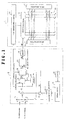
- FIG. 1 illustrates the configuration of a plasma display device as a display device in accordance with the present invention.
- the plasma display device comprises a display unit 1 and a video signal processing unit 2.
- the display unit 1 comprises a PDP 10 as a plasma display panel, an X electrode driver 11, an Y electrode driver 12, an address data driver 13, and a light emission drive control circuit 14.
- Row electrodes D 1 -D m extending in the vertical direction in the display screen are formed in the PDP 10. Further, row electrodes X 1 -X n and row electrodes Y 1 -Y n extending in the horizontal direction of the display screen are also formed with an X-Y alternating configuration in the PDP 10. In this case, the row electrode pairs (Y 1 , X 1 ) , (Y 2 , X 2 ), (Y 3 , X 3 ), ... (Y n , X n ) , in which two adjacent electrodes form a pair, correspond to respective first display line to n-th display line in the PDP 10. A pixel cell PC is formed in the intersections of each display line and each column electrode D 1 -D m .
- the pixel cells PC 1 , 1 to PC 1, m that belong to the first display line, the pixel cells PC 2, 1 to PC 2, m that belong to the second display line, ..., and the pixel cells PC n, 1 to PC n, m that belong to the n-th display line are arranged as a matrix.
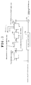
- a light emission drive control circuit 14 controls the X electrode driver 11, Y electrode driver 12, and address data driver 13 so as to light emission drive the PDP 10 according to the light emission drive sequence employing a sub-field method, for example, as shown in FIG. 2.
- each field (or frame) of a video signal comprises 15 sub-fields SF1-SF15 each comprising an address step Wc and a light emission sustained step Ic.
- the Y electrode driver 12 successively applies a scanning pulse SP to row electrodes Y 1 through Y n .
- the address data driver 13 applies to the column electrodes D 1 -D m of the PDP 10 the respective m pixel data pulses DP 1 -DP m having a voltage corresponding to respective pixel drive data bits of one display line supplied from the memory 31.
- Such an operation sets each pixel cell PC 1, 1 to PC n, m of the PDP 10 into either a light emission mode in which light is emitted in the light emission sustained step Ic or a quenching mode in which a quenched state is assumed in the light emission sustained step Ic, according to the pixel drive data bit DB.
- the X electrode driver 11 applies to each row electrode X 1 -X n of the PDP 10 a sustaining pulse with the repetition frequency corresponding to the weight of the sub-field SF.
- the Y electrode driver 12 applies to each row electrode Y 1 -Y n of the PDP 10 a sustaining pulse with the repetition frequency corresponding to the weight of the sub-field.
- the video image processing unit 2 comprises an input selector 21, a display control circuit 22, an adder 23, an OSD (On Screen Display) image signal generation circuit 24, a switch 25, an operation unit 26, an APL detection circuit 27, a luminance adjustment circuit 28, a luminance correction circuit 29, a pixel drive data generation circuit 30, and a memory 31.
- OSD On Screen Display
- the input selector 21 selects either the inputted television video signal (referred to hereinbelow as “TV video signal”) or the inputted computer video signal (referred to hereinbelow as “PC video signal”) according to the selection signal supplied from the display control circuit 22 and supplies the selected signal to the adder 23.
- the OSD image signal generation circuit 24 generates an OSD image signal (on screen image signal) corresponding to the control image designated in the display control circuit 22 and supplies the generated signal to the switch 25.
- the switch 25 is switched ON when the OSD image display command signal OS is supplied from the display control circuit 22 and supplies this OSD image signal to the adder 23.
- the adder 23 adds the OSD image signal supplied from the switch 25 to the video signal (TV video signal or PC video signal) supplied from the input selector 21 and supplies the obtained video signal VS to the light emission drive control circuit 14, APL detection circuit 27, and luminance adjustment circuit 28.
- the operation unit 26 receives the operation instructions from the user and generates various command signals corresponding to those operations. For example, if the user executes the operation so as to display a television video, the operation unit 26 supplies a television video display command signal to the display control circuit 22. At this time, the display control circuit 22 supplies to the input selector 21 the selection signal S for selecting the TV video signals. Further, if the user executes the operation so as to display a computer video, the operation unit 26 supplies a computer video display command signal to the display control circuit 22. At this time, the display control circuit 22 supplies to the input selector 21 the selection signal S for selecting the computer video signals.
- the operation unit 26 supplies to the display control circuit 22 a command requesting the generation of an OSD image signal for screen size switching control and supplies the OSD image display command signal OS to the switch 25.
- the adder 23 superimposes, for example, the OSD image signal for screen size switching control on the video signal (TV video signal or PC video signal) selected by the input selector 21 and outputs the obtained video signal VS. If the user conducted no command operation requesting the display of OSD images, the switch 25 assumes an OFF state. At this time, the adder 23 directly outputs the video signal selected by the input selector 21 as the video signal VS.
- the APL detection circuit 27 finds an average luminance level in this video signal VS for each one field (frame) and supplies it as the average luminance level APL to the luminance adjustment circuit 28.
- the luminance adjustment circuit 28 executes with respect to this video signal VS the adjustment so as to reduce the luminance level of the video signal VS at a reduction rate increasing with the increase in the average luminance level APL and supplies the luminance-adjusted video signal VSc thus obtained to the luminance correction circuit 29.
- the luminance correction circuit 29 conducts the correction processing (described hereinbelow) of the luminance level with respect to the luminance-adjusted video signal VSc so as to correct the luminance nonuniformity resulting from the fact that the magnitude of load corresponding to the total number of pixel cells assuming the light emission state in one display line is different for each pixel line and supplies the luminance-corrected video signal VC thus obtained to the pixel drive data generation circuit 30.
- the pixel drive data generation circuit 30 generates pixel drive data GD 1, 1 - GD n, m designating whether to set the pixel cells PC 1, 1 - PC n, m into a light emission mode or a quenching mode in the address step Wc of each sub-field SFI-SF15 shown in FIG. 2 based on the luminance-corrected video signal VC and supplies those data to the memory 31.
- Each of the pixel drive data GD 1, 1 - GD n, m comprises 15 bits corresponding to sub-fields SF1-SF15.
- the pixel cell PC 1 , 1 is set to the light emission mode in the address step Wc of the sub-field SF1.
- the pixel cell PC 1, 1 is set to the quenching mode in the address step Wc of the sub-field SF1.
- the pixel cell PC 1, 1 is set to the light emission mode in the address step Wc of the sub-field SF15, but when this fifteenth bit is a logical level 0, the pixel cell PC 1, 1 is set to the quenching mode in the address step Wc of the sub-field SF15.
- the memory 31 stores the pixel drive data GD 1,1 -GD n,m supplied from the pixel drive data generation circuit 30 and reads them separately for the columns with identical bits. Thus, the memory 31 reads the pixel drive data GD for each stored pixel cell PC as pixel drive data bits DB1-DB15 as follows:
- the memory 31 reads the pixel drive data bits during execution of the address steps Wc of respective sub-fields as follows:
- FIG. 3 shows the inner configuration of the luminance correction circuit 29.
- a pixel drive data generation circuit 291 first, converts the afore-mentioned luminance-adjusted video signal VSc into pixel data PD 1 -PD m corresponding to each of m pixels located in a display line for each one display line. Then, the pixel drive data generation circuit 291 generates pixel drive data GDD 1 -GDD m each composed of 15 bits for designating the setting state (light emission or quenching mode) of a pixel cell PC in the address steps Wc of corresponding sub-fields SF1-SF15 based on the pixel data PD 1 -PD m .
- the pixel cell PC 1,1 is set to the light emission mode in the address step Wc of the sub-field SF1.
- the pixel cell PC 1,1 is set to a quenching mode in the address step Wc of the sub-field SF1.
- the third bit of the pixel drive data GDD 2 corresponding to the first display line is a logical level 1
- the pixel cell PC 1 , 2 is set to a light emission mode in the address step Wc of the sub-field SF3.
- a light-emitting cell number measurement circuit 292 finds as a light-emitting cell number LN the number of pixel cells PC that will be set to the light emission mode for each sub-field SF1-SF15 based on the pixel drive data GDD 1 -GDD m for one display line. Further, the light-emitting cell number measurement circuit 292 supplies the light-emitting cell numbers LN1-LN15 relating to each sub-field SF1-SF15 to a SF correction coefficient computation circuit 293.
- the SF correction coefficient computation circuit 293 finds the SF correction coefficients SG1-SG15 corresponding to each sub-field SF1-SF15 by the following formula and supplies the SF correction coefficients to a pixel correction coefficient computation circuit 294.
- SG 1 - ⁇ ⁇ [ (m - LN)/m] 2 , where ⁇ : prescribed coefficient; m: total number of pixel cells PC belonging to one display line; LN: number of light-emitting cells in one display line.
- a one display line delay memory 296 delays by one display line the luminance-adjusted video signals supplied from the luminance adjustment circuit 28 and then successively sends them to a multiplier 295.
- the multiplier 295 successively multiplies the pixel correction coefficients G 1 , G 2 , G 3 , ... G m by the luminance level indicated by the luminance-adjusted video signals VSc successively supplied from the one display line delay memory 296 and outputs the multiplication results as luminance-corrected video signals VC.
- the multiplier 295 conducts the correction of the luminance level by successively multiplying the pixel correction coefficients G 1 , G 2 , G 3 , ... G m corresponding to the pixel with respect to the intervals corresponding to each pixel in the luminance-adjusted video signals VSc.
- SF correction coefficients SG1-SG15 corresponding to the number of pixel cell PC that are set in the light emission mode within each display line are found for each sub-field SF1-SF15. Then, weighting addition is executed by adding a weight determined by the number of light emission cycles K1-K15 of each sub-field with respect to each SF correction coefficient SG1-SG15, as shown by the numerator term of the equation Eq.1. At this time, the SF correction coefficient SG that is the object of weighting addition is determined for each pixel based on the pixel drive data GDD (B1-B15) corresponding to the pixel.
- the SF correction coefficient SF of the sub-field SF corresponding to this bit position becomes the object of weighting addition.
- the SF correction coefficient SG of the sub-field SF corresponding to the bit position with a logical level 0 that sets the pixel cell into the quenching mode is outside the range of objects of the above-described weighting addition.
- the luminance correction circuit 29 finds the pixel correction coefficient G of each pixel by dividing the weighting addition results by the total number of light emission cycles within one field based on the pixel drive data GDD, as shown by the equation Eq.1 above.
- the luminance correction circuit 29 generates a luminance-corrected video signal VC, which was subjected to luminance correction, by multiplying the luminance-adjusted video signal VSc by the pixel correction coefficient G of each pixel.
- the magnitude of load of each display line is found by measuring the number of pixel cells PC assuming the light emission state (or quenching state), and the luminance level of the luminance-adjusted video signal VSc corresponding to each pixel cell belonging to the display line is corrected according to this magnitude of load.
- the number pf pixel cell PC assuming the light emission state in each display line decreases, the current consumption in the display lines decreases and the voltage drop also decreases. Therefore, as the number of pixel cells PC assuming the light emission state (on each display line) decreases, the correction is conducted that has to reduce the luminance level of the luminance-adjusted video signal VSc.
- Such a correction reduces the difference in luminance of the pixel cells between a display line where the voltage drop increases because of a large number of pixel cells assuming the light emission state and a display line where the voltage drop is small due to a small number of pixel cells assuming the light emission state.
- the difference in luminance between the display lines can be reduced without conducting a complex control such as changing for each display line the number of sustaining pulses that have to be applied to the PDP 10.
- the SF correction coefficient computation circuit 293 of the luminance correction circuit 29 finds the SF correction coefficients SG1-SG15 corresponding to each one sub-field SF1-SF15 by the following formula.
- SG 1 + ⁇ ⁇ [LN/m] 2 , where ⁇ : prescribed coefficient; m: total number of pixel cells PC on one display line; LN: number of light-emitting cells in one display line.
- the SF correction coefficient SG decreases by the respective number and the pixel correction coefficient G becomes large (1 or more).
- the luminance correction circuit 29 conducts the correction so as to increase the luminance level of the luminance-adjusted video signal VSc.
- the difference in luminance between the display lines is less noticeable than in the case where a bright image is displayed.
- the correction quantity relating to the luminance-adjusted video signal VSc may be decreased by comparison with the case where the average luminance level within one screen is higher than the prescribed level.
- the pixel correction coefficient computation circuit 294 supplies to the multiplier 295 a pixel correction coefficient GG in which the correction quantity relating to the luminance-adjusted video signal VSc was reduced by conducting computation, for example, by the below-described formula, with respect to the pixel correction coefficient G, instead of the pixel correction coefficient G found by the above-described equation Eq.1.
- the pixel correction coefficient computation circuit 294 may fixedly supply "1" at which the correction quantity is 0 to the multiplier 295, instead of the pixel correction coefficient G found by the above-described equation Eq.1.
- the difference in luminance between the display lines is less noticeable than in the case where an OSD image is displayed with superposition on the input video signal, or the case where the input video signal is a PC video signal.
- the pixel correction coefficient computation circuit 294 supplies to the multiplier 295 the pixel correction coefficient GG, in which the correction quantity relating to the luminance-adjusted video signal VSc is less than that in the pixel correction coefficient G, instead of the pixel correction coefficient G found by the above-described equation Eq.1.
- the pixel correction coefficient computation circuit 294 may fixedly supply "1" at which the correction quantity is 0 to the multiplier 295, instead of the pixel correction coefficient G found by the above-described equation Eq.1.
- the magnitude of load is measured for each display line based on the light emission state of each pixel cell on a display line, and the correction of the luminance level according to the magnitude of load corresponding to this display line is conducted with respect to the interval in the video signal that corresponds to each display line.
- the difference in luminance sometimes occurs depending on the mutual arrangement of the pixel cells PC assuming the light emission state.
- the light emission luminance decreases in the pixel cells PC positioned at the left or right end with respect to the central portion of the display line.
- FIG. 4 shows another internal configuration of the luminance correction circuit 29 provided in view of this issue.
- a circuit 298 for measuring the distance between light-emitting cells and a SF correction coefficient generation circuit 299 are used instead of the light-emitting cell number measurement circuit 292 and SF correction coefficient computation circuit 293 shown in FIG. 3.
- Other components are identical to those shown in FIG. 3.
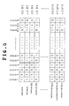
- the circuit 298 for measuring the distance between light-emitting cells measures for each sub-field SF1-SF15 the distance from each pixel cell to the pixel cell in the light emission mode state that is located in the position closest thereto (within one display line) based on the pixel drive data GDD 1 -GDD m of each display line. For example, when the pixel drive data GDD 1 -GDD m have logical levels as shown in FIG. 5, the pixel cells of the first column are set to a light-emission mode in the sub-field SF1 because the first bit B1 of the pixel drive data GDD 1 is a logical level 1.
- both the second bit B2 and the third bit B3 of the pixel drive data GDD 1 corresponding to each image cell of the second column adjacent to the pixel cells of the first column and the third column are a logical level 0, but the fourth bit B4 of the pixel drive data GDD 1 corresponding to the image cell of the fourth column is a logical level 1.
- the pixel cell in the light emission mode state that is located in the position closest to the pixel cell of the first column becomes the pixel cell of the fourth column.
- the circuit 298 for measuring the distance between light-emitting cells.
- the pixel cell in the light emission mode state that is located in the closest position becomes the pixel cell of the first column and, therefore, the distance "1" from this pixel cell of the second column to the pixel cell of the first column will be measured by the circuit 298 for measuring the distance between light-emitting cells.
- the circuit 298 for measuring the distance between light-emitting cells.
- the circuit 298 for measuring the distance between light-emitting cells measures the distance to the light-emitting pixel cell located in the closest position in the same display line for each pixel cell correspondingly to each sub-field SF1-SF15 and supplies the data LD indicating the distance between the light-emitting cells to the SF correction coefficient generation circuit 299.
- the SF correction coefficient generation circuit 299 finds the SF correction coefficients SG1-SG15 having values according to the data LD relating to the distance between the light-emitting cells that correspond to each sub-field SF1-SF15 for each pixel cell and supplies those SF correction coefficients to the pixel correction coefficient computation circuit.
Landscapes
- Engineering & Computer Science (AREA)
- Physics & Mathematics (AREA)
- Computer Hardware Design (AREA)
- General Physics & Mathematics (AREA)
- Theoretical Computer Science (AREA)
- Control Of Indicators Other Than Cathode Ray Tubes (AREA)
- Transforming Electric Information Into Light Information (AREA)
- Control Of Gas Discharge Display Tubes (AREA)
- Control Of El Displays (AREA)
Applications Claiming Priority (2)
| Application Number | Priority Date | Filing Date | Title |
|---|---|---|---|
| JP2004065578 | 2004-03-09 | ||
| JP2004065578A JP2005257754A (ja) | 2004-03-09 | 2004-03-09 | 表示装置 |
Publications (2)
| Publication Number | Publication Date |
|---|---|
| EP1580716A2 true EP1580716A2 (de) | 2005-09-28 |
| EP1580716A3 EP1580716A3 (de) | 2009-09-09 |
Family
ID=34858328
Family Applications (1)
| Application Number | Title | Priority Date | Filing Date |
|---|---|---|---|
| EP05101817A Withdrawn EP1580716A3 (de) | 2004-03-09 | 2005-03-09 | Anzeigegerät |
Country Status (3)
| Country | Link |
|---|---|
| US (1) | US7701415B2 (de) |
| EP (1) | EP1580716A3 (de) |
| JP (1) | JP2005257754A (de) |
Cited By (1)
| Publication number | Priority date | Publication date | Assignee | Title |
|---|---|---|---|---|
| CN102656622A (zh) * | 2009-12-16 | 2012-09-05 | 松下电器产业株式会社 | 等离子显示装置和等离子显示面板的驱动方法 |
Families Citing this family (15)
| Publication number | Priority date | Publication date | Assignee | Title |
|---|---|---|---|---|
| KR100805105B1 (ko) * | 2006-02-28 | 2008-02-21 | 삼성에스디아이 주식회사 | 플라즈마 표시 장치 및 그 구동 방법 |
| JP2007328036A (ja) * | 2006-06-06 | 2007-12-20 | Pioneer Electronic Corp | プラズマディスプレイパネルの駆動方法 |
| JP5134264B2 (ja) * | 2007-03-02 | 2013-01-30 | パナソニック株式会社 | プラズマディスプレイパネルの駆動方法 |
| KR100863964B1 (ko) | 2007-04-12 | 2008-10-16 | 삼성에스디아이 주식회사 | 플라즈마 표시 장치 및 그 구동 방법 |
| JP5191724B2 (ja) * | 2007-12-14 | 2013-05-08 | 株式会社日立製作所 | アドレス駆動回路及びプラズマディスプレイ装置 |
| JP2011149969A (ja) * | 2008-05-14 | 2011-08-04 | Panasonic Corp | プラズマディスプレイ装置およびプラズマディスプレイパネルの駆動方法 |
| JP5188891B2 (ja) * | 2008-06-26 | 2013-04-24 | 篠田プラズマ株式会社 | 発光管アレイ型表示装置及び輝度補正方法 |
| US8576260B2 (en) | 2008-11-12 | 2013-11-05 | Panasonic Corporation | Plasma display device and plasma display panel driving method |
| KR101246413B1 (ko) * | 2008-11-13 | 2013-03-22 | 파나소닉 주식회사 | 플라즈마 디스플레이 장치 및 플라즈마 디스플레이 패널의 구동 방법 |
| US8471786B2 (en) | 2008-11-13 | 2013-06-25 | Panasonic Corporation | Plasma display device and plasma display panel driving method |
| JPWO2011030548A1 (ja) * | 2009-09-11 | 2013-02-04 | パナソニック株式会社 | プラズマディスプレイパネルの駆動方法およびプラズマディスプレイ装置 |
| KR20120060241A (ko) * | 2009-12-14 | 2012-06-11 | 파나소닉 주식회사 | 플라즈마 디스플레이 장치 및 플라즈마 디스플레이 패널의 구동 방법 |
| JP2013003238A (ja) * | 2011-06-14 | 2013-01-07 | Sony Corp | 映像信号処理回路、映像信号処理方法、表示装置、及び、電子機器 |
| CN108269516B (zh) * | 2018-01-24 | 2022-01-25 | 京东方科技集团股份有限公司 | 驱动负载补偿单元、方法、模组和显示装置 |
| CN113077755A (zh) * | 2020-01-06 | 2021-07-06 | 京东方科技集团股份有限公司 | 电致发光显示面板及其驱动方法和显示装置 |
Family Cites Families (23)
| Publication number | Priority date | Publication date | Assignee | Title |
|---|---|---|---|---|
| JP2745548B2 (ja) * | 1988-07-28 | 1998-04-28 | 日本電気株式会社 | プラズマディスプレイの駆動方法 |
| JPH0291687A (ja) * | 1988-09-28 | 1990-03-30 | Nec Corp | 表示装置 |
| JPH0535205A (ja) * | 1991-07-29 | 1993-02-12 | Nec Corp | プラズマデイスプレイの駆動方式 |
| JPH0832903A (ja) * | 1994-07-18 | 1996-02-02 | Pioneer Electron Corp | プラズマディスプレイ装置 |
| JP2757795B2 (ja) * | 1994-12-02 | 1998-05-25 | 日本電気株式会社 | プラズマディスプレイの輝度補償方法及びプラズマディスプレイ装置 |
| JP2964922B2 (ja) * | 1995-07-21 | 1999-10-18 | 株式会社富士通ゼネラル | ディスプレイ装置の駆動回路 |
| JP3103018B2 (ja) | 1995-07-26 | 2000-10-23 | 日立造船株式会社 | 被破壊物の破壊装置および破壊方法 |
| JP3611377B2 (ja) * | 1995-09-01 | 2005-01-19 | 富士通株式会社 | 画像表示装置 |
| JP3636573B2 (ja) | 1997-06-27 | 2005-04-06 | パイオニア株式会社 | 輝度制御装置 |
| US6496194B1 (en) * | 1998-07-30 | 2002-12-17 | Fujitsu Limited | Halftone display method and display apparatus for reducing halftone disturbances occurring in moving image portions |
| JP2000122606A (ja) * | 1998-10-19 | 2000-04-28 | Mitsubishi Electric Corp | Pdp表示装置 |
| JP3642689B2 (ja) * | 1998-12-08 | 2005-04-27 | 富士通株式会社 | プラズマディスプレイパネル装置 |
| EP1049068A1 (de) * | 1999-04-28 | 2000-11-02 | THOMSON multimedia S.A. | Verfahren und Vorrichtung zur Videosignalverarbeitung |
| JP3695737B2 (ja) * | 1999-07-01 | 2005-09-14 | パイオニア株式会社 | プラズマディスプレイパネルの駆動装置 |
| US6559816B1 (en) * | 1999-07-07 | 2003-05-06 | Lg Electronics Inc. | Method and apparatus for erasing line in plasma display panel |
| JP2001067041A (ja) * | 1999-08-31 | 2001-03-16 | Nec Corp | プラズマディスプレイの駆動装置、プラズマディスプレイのサブフィールド変換方法、およびプラズマディスプレイ装置 |
| TW490701B (en) * | 2001-04-04 | 2002-06-11 | Acer Display Tech Inc | Brightness compensation method for plasma display |
| US6630796B2 (en) * | 2001-05-29 | 2003-10-07 | Pioneer Corporation | Method and apparatus for driving a plasma display panel |
| JP4851663B2 (ja) * | 2001-07-19 | 2012-01-11 | パナソニック株式会社 | 表示パネルの輝度制御方法 |
| JP3995504B2 (ja) * | 2002-03-22 | 2007-10-24 | 三洋電機株式会社 | 有機elディスプレイ装置 |
| JP4055679B2 (ja) * | 2003-08-25 | 2008-03-05 | セイコーエプソン株式会社 | 電気光学装置、電気光学装置の駆動方法及び電子機器 |
| KR100563462B1 (ko) * | 2003-10-21 | 2006-03-23 | 엘지전자 주식회사 | 플라즈마 디스플레이 패널의 구동장치 및 방법 |
| KR20050075216A (ko) * | 2004-01-16 | 2005-07-20 | 엘지전자 주식회사 | 플라즈마 표시 패널에서의 로드 이펙트 상쇄 장치 |
-
2004
- 2004-03-09 JP JP2004065578A patent/JP2005257754A/ja active Pending
-
2005
- 2005-03-07 US US11/072,648 patent/US7701415B2/en not_active Expired - Fee Related
- 2005-03-09 EP EP05101817A patent/EP1580716A3/de not_active Withdrawn
Cited By (1)
| Publication number | Priority date | Publication date | Assignee | Title |
|---|---|---|---|---|
| CN102656622A (zh) * | 2009-12-16 | 2012-09-05 | 松下电器产业株式会社 | 等离子显示装置和等离子显示面板的驱动方法 |
Also Published As
| Publication number | Publication date |
|---|---|
| US7701415B2 (en) | 2010-04-20 |
| EP1580716A3 (de) | 2009-09-09 |
| JP2005257754A (ja) | 2005-09-22 |
| US20050200571A1 (en) | 2005-09-15 |
Similar Documents
| Publication | Publication Date | Title |
|---|---|---|
| EP1580716A2 (de) | Anzeigegerät | |
| JP4165710B2 (ja) | プラズマディスプレイパネルの画像表示方法およびその装置 | |
| KR100647688B1 (ko) | 플라즈마 디스플레이 패널 구동방법 | |
| KR20090058822A (ko) | 삼차원 영상에 대한 디스플레이 장치 및 디스플레이 방법 | |
| KR100603297B1 (ko) | 패널 구동 방법, 패널 구동 장치 및 디스플레이 패널 | |
| JP2000035774A (ja) | 表示装置 | |
| JP4611880B2 (ja) | プラズマ表示装置およびプラズマ表示装置の画像処理方法 | |
| US7453422B2 (en) | Plasma display panel having an apparatus and method for displaying pictures | |
| KR100521471B1 (ko) | 서브필드 위치 변동 방지를 위한 플라즈마 디스플레이패널의 구동 방법 및 그 장치 | |
| JP2000347620A (ja) | 表示装置 | |
| JP4965825B2 (ja) | 表示装置 | |
| JP2005078098A (ja) | プラズマディスプレイパネルのアドレス電力制御方法及びその装置 | |
| KR100898299B1 (ko) | 플라즈마 표시 장치 및 그 구동 방법 | |
| JP4165108B2 (ja) | プラズマディスプレイ装置 | |
| KR100590102B1 (ko) | 플라즈마 표시 장치 및 그 구동 방법 | |
| KR100578917B1 (ko) | 플라즈마 디스플레이 패널의 구동 장치, 플라즈마디스플레이 패널의 화상 처리 방법 및 플라즈마디스플레이 패널 | |
| JP2006301556A (ja) | 表示装置 | |
| KR100551058B1 (ko) | 플라즈마 디스플레이 패널의 구동 장치 및 그 구동 방법 | |
| JP4887363B2 (ja) | プラズマディスプレイ装置 | |
| KR100529104B1 (ko) | 플라즈마 디스플레이 패널 및 그의 구동 방법 | |
| KR100536220B1 (ko) | 플라즈마 디스플레이 패널의 구동 장치, 플라즈마디스플레이 패널의 화상 처리 방법 및 플라즈마디스플레이 패널 | |
| KR100560486B1 (ko) | 플라즈마 표시 장치 및 그 화상 처리 방법 | |
| KR100626084B1 (ko) | 디스플레이 패널의 구동방법 및 그 장치 | |
| KR100553767B1 (ko) | 플라즈마 디스플레이 패널의 구동방법 및 구동장치 | |
| KR20040082802A (ko) | 플라즈마 디스플레이 패널의 구동 장치 및 그 방법 |
Legal Events
| Date | Code | Title | Description |
|---|---|---|---|
| PUAI | Public reference made under article 153(3) epc to a published international application that has entered the european phase |
Free format text: ORIGINAL CODE: 0009012 |
|
| AK | Designated contracting states |
Kind code of ref document: A2 Designated state(s): AT BE BG CH CY CZ DE DK EE ES FI FR GB GR HU IE IS IT LI LT LU MC NL PL PT RO SE SI SK TR |
|
| AX | Request for extension of the european patent |
Extension state: AL BA HR LV MK YU |
|
| PUAL | Search report despatched |
Free format text: ORIGINAL CODE: 0009013 |
|
| RAP1 | Party data changed (applicant data changed or rights of an application transferred) |
Owner name: PANASONIC CORPORATION |
|
| AK | Designated contracting states |
Kind code of ref document: A3 Designated state(s): AT BE BG CH CY CZ DE DK EE ES FI FR GB GR HU IE IS IT LI LT LU MC NL PL PT RO SE SI SK TR |
|
| AX | Request for extension of the european patent |
Extension state: AL BA HR LV MK YU |
|
| 17P | Request for examination filed |
Effective date: 20100309 |
|
| AKX | Designation fees paid |
Designated state(s): DE FR GB |
|
| 17Q | First examination report despatched |
Effective date: 20100503 |
|
| STAA | Information on the status of an ep patent application or granted ep patent |
Free format text: STATUS: THE APPLICATION IS DEEMED TO BE WITHDRAWN |
|
| 18D | Application deemed to be withdrawn |
Effective date: 20131001 |