EP1579487B1 - Verfahren zur herstellung eines halbleiterbauelements - Google Patents
Verfahren zur herstellung eines halbleiterbauelements Download PDFInfo
- Publication number
- EP1579487B1 EP1579487B1 EP03813689A EP03813689A EP1579487B1 EP 1579487 B1 EP1579487 B1 EP 1579487B1 EP 03813689 A EP03813689 A EP 03813689A EP 03813689 A EP03813689 A EP 03813689A EP 1579487 B1 EP1579487 B1 EP 1579487B1
- Authority
- EP
- European Patent Office
- Prior art keywords
- layer
- silicon
- monocrystalline
- region
- arsenic
- Prior art date
- Legal status (The legal status is an assumption and is not a legal conclusion. Google has not performed a legal analysis and makes no representation as to the accuracy of the status listed.)
- Expired - Lifetime
Links
Images

Classifications
-
- H—ELECTRICITY
- H10—SEMICONDUCTOR DEVICES; ELECTRIC SOLID-STATE DEVICES NOT OTHERWISE PROVIDED FOR
- H10P—GENERIC PROCESSES OR APPARATUS FOR THE MANUFACTURE OR TREATMENT OF DEVICES COVERED BY CLASS H10
- H10P14/00—Formation of materials, e.g. in the shape of layers or pillars
- H10P14/20—Formation of materials, e.g. in the shape of layers or pillars of semiconductor materials
- H10P14/34—Deposited materials, e.g. layers
- H10P14/3402—Deposited materials, e.g. layers characterised by the chemical composition
- H10P14/3404—Deposited materials, e.g. layers characterised by the chemical composition being Group IVA materials
- H10P14/3408—Silicon carbide
-
- H—ELECTRICITY
- H10—SEMICONDUCTOR DEVICES; ELECTRIC SOLID-STATE DEVICES NOT OTHERWISE PROVIDED FOR
- H10P—GENERIC PROCESSES OR APPARATUS FOR THE MANUFACTURE OR TREATMENT OF DEVICES COVERED BY CLASS H10
- H10P14/00—Formation of materials, e.g. in the shape of layers or pillars
- H10P14/20—Formation of materials, e.g. in the shape of layers or pillars of semiconductor materials
- H10P14/27—Formation of materials, e.g. in the shape of layers or pillars of semiconductor materials using selective deposition, e.g. simultaneous growth of monocrystalline and non-monocrystalline semiconductor materials
- H10P14/271—Formation of materials, e.g. in the shape of layers or pillars of semiconductor materials using selective deposition, e.g. simultaneous growth of monocrystalline and non-monocrystalline semiconductor materials characterised by the preparation of substrate for selective deposition
- H10P14/272—Formation of materials, e.g. in the shape of layers or pillars of semiconductor materials using selective deposition, e.g. simultaneous growth of monocrystalline and non-monocrystalline semiconductor materials characterised by the preparation of substrate for selective deposition using mask materials other than SiO2 or SiN
-
- H—ELECTRICITY
- H10—SEMICONDUCTOR DEVICES; ELECTRIC SOLID-STATE DEVICES NOT OTHERWISE PROVIDED FOR
- H10P—GENERIC PROCESSES OR APPARATUS FOR THE MANUFACTURE OR TREATMENT OF DEVICES COVERED BY CLASS H10
- H10P14/00—Formation of materials, e.g. in the shape of layers or pillars
- H10P14/20—Formation of materials, e.g. in the shape of layers or pillars of semiconductor materials
- H10P14/34—Deposited materials, e.g. layers
- H10P14/3402—Deposited materials, e.g. layers characterised by the chemical composition
- H10P14/3404—Deposited materials, e.g. layers characterised by the chemical composition being Group IVA materials
- H10P14/3411—Silicon, silicon germanium or germanium
Definitions
- the invention relates to a method of manufacturing a semiconductor device, in which on a region of silicon oxide situated next to a region of monocrystalline silicon at a surface of a semiconductor body, a non-monocrystalline auxiliary layer is formed.
- Said region of silicon oxide may in this case be, for example, a layer of silicon oxide situated on the semiconductor body or a silicon oxide region, such as a field insulation region, recessed in the semiconductor body.
- the auxiliary layer is useful, in particular, in processes where a silicon-containing layer is deposited and where it is desirable that this layer grows as a monocrystalline layer on the region of monocrystalline silicon, and as an amorphous or polycrystalline layer on the region of silicon oxide.
- Said auxiliary layer enhances the growth of the silicon-containing layer on the region of silicon oxide, as a result of which the deposition process can be carried out at such a low temperature that it is precluded that in the course of this deposition process, atoms of dopants provided in the active regions move as a result of diffusion. This is important, in particular, for the manufacture of semiconductor devices with extremely small transistors.
- the silicon-containing layer may be a layer that contains only silicon, but it may also be a layer that, in addition to silicon, contains germanium. Said silicon-containing layer may also comprise sub-layers which are deposited one on top of the other, one sub-layer comprising, for example, only silicon and the other sub-layer comprising, in addition to silicon, germanium. Moreover, the layer or one or more of the sub-layers may be doped with atoms of a customary dopant.
- the base of a bipolar transistor may be formed, which base can be electrically contacted by the adjoining amorphous or polycrystalline layer formed on the regions of silicon oxide.
- WO 00/17423 describes a method of the type mentioned in the opening paragraph wherein a layer of silicon nitride is used as the auxiliary layer.
- Said auxiliary layer is provided by covering the entire surface of the silicon body, on which border regions of monocrystalline silicon, here active semiconductor regions, and regions of silicon oxide, here field insulation regions, with a layer of silicon nitride, after which a photoresist mask is provided having windows within which the active regions are not covered, and by subsequently etching away the parts of the silicon nitride layer that are not covered by the photoresist mask.
- a layer of silicon is deposited on the surface, which silicon layer grows as a monocrystalline layer on the region of monocrystalline silicon, and as a polycrystalline layer on the region of silicon oxide.
- the method in accordance with the invention is characterized in that the auxiliary layer is formed in two process steps, in which, in the course of the first process step, a layer of arsenic is formed on the region of monocrystalline silicon by heating the semiconductor body in an atmosphere with an arsenic compound, and, in the course of the second process step, a layer of non-monocrystalline silicon is formed as an auxiliary layer on the region of silicon oxide by heating the semiconductor body in an atmosphere comprising a gaseous silicon compound instead of a gaseous arsenic compound.
- a layer of non-monocrystalline silicon is formed as an auxiliary layer on the region of silicon oxide by heating the semiconductor body in an atmosphere without gaseous arsenic compound but with a gaseous silicon compound
- the deposition of an amorphous or polycrystalline layer of silicon on the region of silicon oxide starts immediately, while during a certain nucleation time, no deposition takes place on the arsenic-covered region of monocrystalline silicon.
- An auxiliary layer of amorphous or polycrystalline silicon can thus be formed in a self-aligning manner, which completely covers the silicon oxide region and leaves the monocrystalline silicon region completely exposed. If a silicon-containing layer is subsequently deposited on a surface thus prepared, then growth starts immediately on the monocrystalline silicon region as well as on the silicon oxide region. The monocrystalline and non-monocrystalline layers then deposited blend seamlessly.
- a simple method is obtained if during the formation of the auxiliary layer, the semiconductor body is heated during the first process step in an atmosphere comprising, in addition to the gaseous arsenic compound, the gaseous silicon compound used during the second process step.
- the semiconductor body is heated during the first process step in an atmosphere comprising, in addition to the gaseous arsenic compound, the gaseous silicon compound used during the second process step.
- the supply of gaseous arsenic compound has to be stopped.
- this silicon compound does not influence the formation of the layer of arsenic.
- the second process step is ended before deposition from the silicon compound takes place on the arsenic layer formed on the regions of monocrystalline silicon.
- the deposition process of the auxiliary layer is stopped before the nucleation time has ended. After this nucleation time, a layer starts forming also on the regions of monocrystalline silicon. These must be etched away since they would hamper the growth of monocrystalline silicon. It is simpler to stop the deposition process in time, i.e. within said nucleation time.
- the semiconductor body is heated during both process steps at a temperature in the range between 400 and 600 °C in an atmosphere with a pressure below 67 Pa (500 mTorr), then the above-mentioned nucleation time is more than approximately 5 minutes, during which period of time an approximately 10 nm thick auxiliary layer of low-amorphous silicon can be formed.
- the monoatomic layer of arsenic can be removed before a silicon-containing layer is deposited.
- a silicon-containing layer can be deposited on the layer of arsenic and the adjacent auxiliary layer of non-monocrystalline silicon without the growth of such a layer being adversely affected by the presence of the layer of arsenic.
- a layer of Si i-x Ge x where 0.05 ⁇ x ⁇ 0.20 and to which less than 0.2 at.% carbon has been added, can be directly deposited on the layer of arsenic and the adjoining auxiliary layer by heating the semiconductor body in an atmosphere with a silicon compound and a germanium compound.
- an n-type semiconductor zone is formed in the region of monocrystalline silicon, then the arsenic layer is formed on the n-type semiconductor zone.
- a semiconductor zone is formed having a relatively heavily doped surface. This is advantageous, in particular, if an n-type collector zone of a bipolar transistor is formed in the regions of monocrystalline silicon and, in the monocrystalline layer deposited thereon, a p-type base zone of this transistor is formed. In absolute terms, the p-type base zone is more heavily doped than the n-type collector zone formed in the active regions.
- the pn-junction will be situated between collector and base in the deposited monocrystalline layer. Without said arsenic layer, this pn-junction would be formed below the deposited monocrystalline layer in the collector zone, as a result of which a thicker base and hence a slower transistor would be formed.
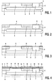
- Figs. 1 through 8 are diagrammatic, cross-sectional views of several stages in the manufacture of a semiconductor device with a bipolar npn-transistor. For simplicity, the Figures merely show the manufacture of a single transistor. It will be understood that, in practice, a semiconductor device with an integrated circuit may comprise very many such transistors as well as transistors of different types.
- a semiconductor body of silicon 1 is taken as a basis, which as shown in Fig. 1 is provided with an epitaxially grown layer 2 that is n-type doped with approximately 5.10 15 atoms per cm 3 .
- a region of monocrystalline silicon, here an active region 4, and silicon oxide regions, here field insulation regions 5, bordering on said active region 4 are formed in said layer 2 so as to border on a surface 3 thereof.
- a buried layer 6 that is n-type doped with approximately 10 20 atoms per cm 3 and a contact zone 7 bordering on the surface 3 and n-type doped with approximately 10 19 atoms per cm 3 are formed in a customary manner.
- n-type doping with approximately 10 18 atoms per cm 3 (not shown). This reaches as far as the buried layer 6 but leaves the doping of the epitaxially formed layer 2 unchanged near the surface 3. This doping serves to improve the contacting to the transistor's collector to be formed near the surface 3.
- a silicon-containing layer will be deposited on the surface 3, which silicon-containing layer grows in a monocrystalline manner on the monocrystalline active region 4 and in a non-monocrystalline (amorphous or polycrystalline) manner on the insulation regions 5.
- this layer may also comprise germanium.
- This layer may further comprise sub-layers deposited one on top of the other, in which case, for example, one sub-layer comprises only silicon and the other sub-layer comprises silicon and germanium.
- an auxiliary layer 8 is formed on the insulation regions to enhance the growth of the silicon-containing layer there.
- the deposition process can be carried out at a comparatively low temperature below 700 °C. It is thus precluded that atoms of dopants provided in the active regions migrate as a result of diffusion, as would occur, for example, in the case of the n-type doping provided in the active region 4 to improve the contacting to the collector zone to be formed.
- the auxiliary layer 8 is formed in two steps by means of a customary LPCVD process at a temperature between 400 and 600 °C and a pressure below 93.3 Pa (700 mTorr), in this example a temperature of 550 °C and a pressure of 80.0 Pa (600 mTorr).
- the semiconductor body 1 is heated in an atmosphere comprising a gaseous arsenic compound and, in this example, also a gaseous silicon compound, and during the second step it is heated in an atmosphere without gaseous arsenic compound but with the same gaseous silicon compound as during the first step.
- the slice 1 is placed in a reaction chamber through which, during the first step, a gas mixture is passed for three minutes which, as well as a non-reactive carrier gas such as nitrogen, comprises arsine and silane, and during the second step, a gas mixture comprising, in addition to a non-reactive carrier gas, only silane is passed through said reaction chamber for approximately 10 minutes.
- a gas mixture is passed for three minutes which, as well as a non-reactive carrier gas such as nitrogen, comprises arsine and silane
- a gas mixture comprising, in addition to a non-reactive carrier gas, only silane is passed through said reaction chamber for approximately 10 minutes.
- the gas mixture that is passed through the reaction chamber would not have to contain a silicon compound. This compound, however, does not influence the deposition of arsenic. In this example a simpler deposition process has been chosen in which, after the first step, the supply of the arsenic compound only has to be stopped.
- a layer of arsenic forms on the monocrystalline silicon of the active region 4 and the contact region 7, as schematically indicated in Fig. 2 by means of dashed line 9, while no arsenic is deposited on the insulation regions of silicon oxide 5.
- This process stops automatically when a closed monoatomic layer of arsenic has formed in approximately 3 minutes on the active region 4 and the contact region 7.
- the deposition of amorphous silicon on the insulation regions 5 starts immediately, while during a certain nucleation time of approximately 10 minutes, no deposition takes place on the arsenic-coated active regions 4 and 7. In this manner, the auxiliary layer 8 is formed only on the insulation regions 5 in a self-aligning manner.
- the second step is terminated prior to the deposition of silicon on the arsenic layer 9 formed on the active region 4 in the first step.
- the deposition process of the auxiliary layer is then stopped before the nucleation time has ended. After this nucleation time a layer of amorphous silicon starts forming also on the active regions. Within said ten minutes of nucleation time, as shown in Fig. 3 , an approximately 10 nm thick auxiliary layer of amorphous silicon is formed on the insulation regions 5.
- a silicon-containing double layer 10, 11 and 13, 14 is deposited, as shown in Fig. 4 , in a customary manner at a temperature below 700 °C and a pressure below 6.7 kPa (50 Torr).
- a silicon-containing double layer 10, 11 and 13, 14 is deposited, as shown in Fig. 4 , in a customary manner at a temperature below 700 °C and a pressure below 6.7 kPa (50 Torr).
- a silicon-containing double layer 10, 11 and 13, 14 is deposited, as shown in Fig. 4 , in a customary manner at a temperature below 700 °C and a pressure below 6.7 kPa (50 Torr).
- a gas mixture comprising, in addition to a non-reactive carrier gas, silane, germanium and carbon dioxide.
- diborane is added to this gas mixture for a short period of time.
- a layer 10, 11 is thus deposited which, as indicated by means of a dashed line 12, is provided with an intermediate layer which is p-type doped with boron ions.
- a monocrystalline layer 10 is formed on the active region 4; a polycrystalline layer 11 is formed on the auxiliary layer 8 formed on the insulation regions 5.
- a monocrystalline layer 10 is formed also on the contact regions 7.
- an approximately 30 nm thick layer 13, 14 of silicon is subsequently deposited in this example.
- a gas mixture comprising, in addition to a non-reactive carrier gas, silane is passed through the reaction chamber.
- a monocrystalline layer of silicon 13 is formed, and on the polycrystalline layer 11 formed on the auxiliary layer 8, a polycrystalline layer of silicon 14 is formed.
- a monocrystalline layer of silicon 13 is formed on the contact regions 7, also a monocrystalline layer of silicon 13 is formed.
- the growth on the active regions 4 and the insulation regions 5 starts at the same time.
- the monocrystalline layer 10 and non-monocrystalline layer 11 thus formed are deposited in a substantially equal thickness and thus blend seamlessly. Also the layers 13 and 14 formed thereon blend seamlessly.
- a layer of silicon oxide 15 is deposited, as shown in Fig. 5 , wherein a window 16 is etched in a customary manner at the location of the active region 4, within which window the deposited layer of monocrystalline silicon 11 is exposed.
- a conductor track 17 of n-type doped polycrystalline silicon is subsequently provided, which contacts the layer 13 through the window 16.
- the insulating layer of silicon oxide 15 is etched away, using the conductor track 17 as a mask, and boron ions are implanted in the silicon layer 13, 14, as indicated by means of a dashed line 18, using the conductor track 17 as a mask.
- the deposited layers 10, 11, 13, 14 are subsequently patterned in a customary manner. Above the active region 4 and above an edge of the insulating regions 5 bordering on said region, the layers 10, 11, 13, 14 are maintained, while they are removed from the surface 3 at locations next to said edge.
- a base zone 19 and a base connection 20, as shown in Fig. 8 are formed by diffusion of, respectively, the ions 12 and 18 provided in the layers 10, 11, 13, 14.
- an emitter zone 21 is formed in the layer of monocrystalline silicon 13.
- the part of the active region 4 situated just below the surface 3 forms the collector zone 22 of the transistor.
- the conductor track 17, the base connection zone 20 and the contact zone 7 are provided with a top layer of titanium disilicide, not shown, after which a relatively thick layer of silicon oxide 23 is deposited on the structure thus formed, as shown in Fig. 8 , in which windows 24, 25 and 26 are subsequently formed for contacting, respectively, the base zone 19 (via the base connection zone 20), the emitter zone 21 and the collector zone 22 (via the buried layer 6 and the contact zone 7).
- the monoatomic layer of arsenic 9 can be removed. This does not take place in this example.
- the silicon-containing double layer 10, 11; 13, 14 is deposited on the monoatomic arsenic layer 9.
- the active region 4 bordering on the surface 3 and forming the collector zone 22 of the transistor obtains a comparatively high n-type doping.
- the p-type base zone 19 is higher doped than the n-type collector zone 22.
Landscapes
- Bipolar Transistors (AREA)
- Recrystallisation Techniques (AREA)
- Glass Compositions (AREA)
- Transition And Organic Metals Composition Catalysts For Addition Polymerization (AREA)
- Mechanical Treatment Of Semiconductor (AREA)
Claims (7)
- Verfahren zur Herstellung einer Halbleitervorrichtung, bei dem auf einem Gebiet aus Siliziumoxids, das benachbart zu einem Gebiet monokristallinen Siliziums an einer Oberfläche eines Halbleiterkörpers angeordnet ist, eine nichtmonokristalline Zusatzschicht ausgebildet wird, dadurch gekennzeichnet, dass die Zusatzschicht in zwei Prozessschritten ausgebildet wird, in denen im Verlauf des ersten Prozessschritts eine Schicht aus Arsen nur auf dem Gebiet aus monokristallinem Silizium durch Erhitzen des Halbleiterkörpers in einer Atmosphäre mit einer Arsenverbindung ausgebildet wird, und im Verlauf des zweiten Prozessschritts eine Schicht aus nicht-monokristallinem Silizium als Zusatzschicht nur auf dem Gebiet aus Siliziumoxid mittels Erhitzen des Halbleiterkörpers in einer Atmosphäre, die eine gasförmige Siliziumverbindung anstelle einer gasförmigen Arsenverbindung umfasst, ausgebildet wird.
- Verfahren nach Anspruch 1, dadurch gekennzeichnet, dass während der Ausbildung der Zusatzschicht der Halbleiterkörper während des ersten Prozessschritts in einer Atmosphäre erhitzt wird, die zusätzlich zu der gasförmigen Arsenverbindung die gasförmige Siliziumverbindung enthält, die während des zweiten Prozessschritts verwendet wird.
- Verfahren nach Anspruch 1 oder 2, dadurch gekennzeichnet, dass der zweite Prozessschritt beendet ist, bevor ein Ablagern der Siliziumverbindung auf der auf dem Gebiet des monokristallinen Siliziums gebildeten Arsenschicht stattfindet.
- Verfahren nach Anspruch 1 , 2 oder 3, dadurch gekennzeichnet, dass während des Ausbildens der Zusatzschicht der Halbleiterkörper während beider Prozessschritte bei einer Temperatur im Bereich zwischen 400 und 600 °C in einer Atmosphäre mit einem Druck unterhalb von 67 Pa erhitzt wird.
- Verfahren nach irgendeinem der vorangehenden Ansprüche, dadurch gekennzeichnet, dass nach dem Ausbilden der Zusatzschicht eine siliziumhaltige Schicht auf der Arsenschicht und der Zusatzschicht abgelagert wird, indem der Halbleiterkörper in einer Atmosphäre erhitzt wird, die eine Siliziumverbindung enthält.
- Verfahren nach Anspruch 5, dadurch gekennzeichnet, dass als siliziumhaltige Schicht eine Schicht aus Si1-xGex abgelagert wird, wobei 0,05 < x < 0,20 gilt, zu der weniger als 0,2 Atomprozent Kohlenstoff hinzugefügt ist, indem der Halbleiterkörper in einer Atmosphäre erhitzt wird, die eine Siliziumverbindung und eine Germaniumverbindung umfasst.
- Verfahren nach Anspruch 5 oder 6, dadurch gekennzeichnet, dass im Gebiet aus monokristallinen Silizium eine n-Typ-Kollektorzone eines Bipolartransistors ausgebildet wird, wobei in der monokristallinen Schicht aus Si1-xGex, die darauf abgelagert wird, eine p-Typ-Basiszone dieses Transistors ausgebildet wird.
Priority Applications (1)
| Application Number | Priority Date | Filing Date | Title |
|---|---|---|---|
| EP03813689A EP1579487B1 (de) | 2002-12-20 | 2003-12-16 | Verfahren zur herstellung eines halbleiterbauelements |
Applications Claiming Priority (4)
| Application Number | Priority Date | Filing Date | Title |
|---|---|---|---|
| EP02080509 | 2002-12-20 | ||
| EP02080509 | 2002-12-20 | ||
| PCT/IB2003/006017 WO2004057654A2 (en) | 2002-12-20 | 2003-12-16 | Method of manufacturing a semiconductor device |
| EP03813689A EP1579487B1 (de) | 2002-12-20 | 2003-12-16 | Verfahren zur herstellung eines halbleiterbauelements |
Publications (2)
| Publication Number | Publication Date |
|---|---|
| EP1579487A2 EP1579487A2 (de) | 2005-09-28 |
| EP1579487B1 true EP1579487B1 (de) | 2009-09-23 |
Family
ID=32668808
Family Applications (1)
| Application Number | Title | Priority Date | Filing Date |
|---|---|---|---|
| EP03813689A Expired - Lifetime EP1579487B1 (de) | 2002-12-20 | 2003-12-16 | Verfahren zur herstellung eines halbleiterbauelements |
Country Status (10)
| Country | Link |
|---|---|
| US (1) | US7794540B2 (de) |
| EP (1) | EP1579487B1 (de) |
| JP (1) | JP2006511084A (de) |
| KR (1) | KR20050084387A (de) |
| CN (1) | CN100358110C (de) |
| AT (1) | ATE443925T1 (de) |
| AU (1) | AU2003303274A1 (de) |
| DE (1) | DE60329421D1 (de) |
| TW (1) | TW200501267A (de) |
| WO (1) | WO2004057654A2 (de) |
Family Cites Families (28)
| Publication number | Priority date | Publication date | Assignee | Title |
|---|---|---|---|---|
| JPS61242073A (ja) * | 1985-04-19 | 1986-10-28 | Fujitsu Ltd | 半導体装置の製造方法 |
| JPS63274175A (ja) * | 1987-05-01 | 1988-11-11 | Nippon Telegr & Teleph Corp <Ntt> | ヘテロ接合素子及びその製造方法 |
| JPS6477167A (en) * | 1987-09-18 | 1989-03-23 | Nippon Telegraph & Telephone | Hetero-bipolar transistor |
| JPS6476763A (en) * | 1987-09-18 | 1989-03-22 | Nec Corp | Manufacture of semiconductor device |
| JP2694957B2 (ja) * | 1988-01-14 | 1997-12-24 | 株式会社東芝 | 半導体装置の製造方法 |
| JPH01191412A (ja) * | 1988-01-27 | 1989-08-01 | Oki Electric Ind Co Ltd | 半導体装置の製造方法 |
| JPH0268935A (ja) * | 1988-09-05 | 1990-03-08 | Nippon Telegr & Teleph Corp <Ntt> | 半導体装置 |
| DE4102888A1 (de) * | 1990-01-31 | 1991-08-01 | Toshiba Kawasaki Kk | Verfahren zur herstellung eines miniaturisierten heterouebergang-bipolartransistors |
| US5110757A (en) * | 1990-12-19 | 1992-05-05 | North American Philips Corp. | Formation of composite monosilicon/polysilicon layer using reduced-temperature two-step silicon deposition |
| DE59010916D1 (de) * | 1990-12-21 | 2000-11-30 | Siemens Ag | Verfahren zur Herstellung einer mit Arsen dotierten glatten polykristallinen Siliziumschicht für höchstintegrierte Schaltungen |
| JP3158259B2 (ja) * | 1992-01-29 | 2001-04-23 | 株式会社東芝 | 成膜方法 |
| JPH05251347A (ja) * | 1992-01-29 | 1993-09-28 | Toshiba Corp | 成膜方法 |
| JPH05217916A (ja) * | 1992-01-31 | 1993-08-27 | Nec Corp | 半導体装置の製造方法 |
| US5491107A (en) * | 1993-01-21 | 1996-02-13 | Micron Technology, Inc. | Semiconductor processing method for providing large grain polysilicon films |
| JP2655052B2 (ja) * | 1993-10-07 | 1997-09-17 | 日本電気株式会社 | 半導体装置およびその製造方法 |
| JPH07142505A (ja) * | 1993-11-22 | 1995-06-02 | Sanyo Electric Co Ltd | 半導体装置の製造方法 |
| JP3172031B2 (ja) * | 1994-03-15 | 2001-06-04 | 株式会社東芝 | 半導体装置の製造方法 |
| JP2788984B2 (ja) * | 1995-10-18 | 1998-08-20 | 工業技術院長 | 有機単分子薄膜の製造方法 |
| US5792700A (en) * | 1996-05-31 | 1998-08-11 | Micron Technology, Inc. | Semiconductor processing method for providing large grain polysilicon films |
| FR2774509B1 (fr) * | 1998-01-30 | 2001-11-16 | Sgs Thomson Microelectronics | Procede de depot d'une region de silicium monocristallin |
| FR2779571B1 (fr) * | 1998-06-05 | 2003-01-24 | St Microelectronics Sa | Procede de dopage selectif du collecteur intrinseque d'un transistor bipolaire vertical a base epitaxiee |
| FR2779572B1 (fr) * | 1998-06-05 | 2003-10-17 | St Microelectronics Sa | Transistor bipolaire vertical a faible bruit et procede de fabrication correspondant |
| JP3549408B2 (ja) * | 1998-09-03 | 2004-08-04 | 松下電器産業株式会社 | バイポーラトランジスタ |
| DE19845792A1 (de) | 1998-09-21 | 2000-03-23 | Inst Halbleiterphysik Gmbh | Verfahren zur Erzeugung einer amorphen oder polykristallinen Schicht auf einem Isolatorgebiet |
| US6344673B1 (en) * | 1999-07-01 | 2002-02-05 | International Business Machines Corporation | Multilayered quantum conducting barrier structures |
| KR101027485B1 (ko) * | 2001-02-12 | 2011-04-06 | 에이에스엠 아메리카, 인코포레이티드 | 반도체 박막 증착을 위한 개선된 공정 |
| US6586297B1 (en) * | 2002-06-01 | 2003-07-01 | Newport Fab, Llc | Method for integrating a metastable base into a high-performance HBT and related structure |
| US6847089B2 (en) * | 2003-04-03 | 2005-01-25 | Texas Instruments Incorporated | Gate edge diode leakage reduction |
-
2003
- 2003-12-16 CN CNB2003801071112A patent/CN100358110C/zh not_active Expired - Fee Related
- 2003-12-16 AT AT03813689T patent/ATE443925T1/de not_active IP Right Cessation
- 2003-12-16 JP JP2004561870A patent/JP2006511084A/ja active Pending
- 2003-12-16 US US10/539,549 patent/US7794540B2/en active Active
- 2003-12-16 KR KR1020057011210A patent/KR20050084387A/ko not_active Ceased
- 2003-12-16 WO PCT/IB2003/006017 patent/WO2004057654A2/en not_active Ceased
- 2003-12-16 AU AU2003303274A patent/AU2003303274A1/en not_active Abandoned
- 2003-12-16 EP EP03813689A patent/EP1579487B1/de not_active Expired - Lifetime
- 2003-12-16 DE DE60329421T patent/DE60329421D1/de not_active Expired - Lifetime
- 2003-12-17 TW TW092135803A patent/TW200501267A/zh unknown
Also Published As
| Publication number | Publication date |
|---|---|
| WO2004057654A3 (en) | 2004-10-14 |
| EP1579487A2 (de) | 2005-09-28 |
| JP2006511084A (ja) | 2006-03-30 |
| WO2004057654A2 (en) | 2004-07-08 |
| US7794540B2 (en) | 2010-09-14 |
| CN1729555A (zh) | 2006-02-01 |
| DE60329421D1 (de) | 2009-11-05 |
| KR20050084387A (ko) | 2005-08-26 |
| CN100358110C (zh) | 2007-12-26 |
| US20060148257A1 (en) | 2006-07-06 |
| AU2003303274A1 (en) | 2004-07-14 |
| TW200501267A (en) | 2005-01-01 |
| ATE443925T1 (de) | 2009-10-15 |
Similar Documents
| Publication | Publication Date | Title |
|---|---|---|
| US9508824B2 (en) | Method for fabricating a bipolar transistor having self-aligned emitter contact | |
| US6436781B2 (en) | High speed and low parasitic capacitance semiconductor device and method for fabricating the same | |
| US6756604B2 (en) | Si-Ge base heterojunction bipolar device | |
| US6812545B2 (en) | Epitaxial base bipolar transistor with raised extrinsic base | |
| US5846867A (en) | Method of producing Si-Ge base heterojunction bipolar device | |
| US5620908A (en) | Manufacturing method of semiconductor device comprising BiCMOS transistor | |
| KR100486304B1 (ko) | 자기정렬을 이용한 바이씨모스 제조방법 | |
| US20020003286A1 (en) | Vertical bipolar transistor including an extrinsic base with reduced roughness, and fabrication process | |
| US7105415B2 (en) | Method for the production of a bipolar transistor | |
| US5420053A (en) | Method for manufacturing semiconductor device having bipolar transistor and polycrystalline silicon resistor | |
| WO2000013227A2 (en) | Method of manufacturing a semiconductor device with a bipolar transistor | |
| EP2038918B1 (de) | Verfahren zur herstellung eines bipolaren transistors und in diesem verfahren hergestellter bipolarer transistor | |
| US6417058B1 (en) | SiGe/poly for low resistance extrinsic base npn transistor | |
| US6744080B2 (en) | Method of manufacturing a bipolar transistor of double-polysilicon, heterojunction-base type and corresponding transistor | |
| US6228733B1 (en) | Non-selective epitaxial depostion technology | |
| US5523614A (en) | Bipolar transistor having enhanced high speed operation through reduced base leakage current | |
| US20010005035A1 (en) | Bipolar transistor having lightly doped epitaxial collector region constant in dopant impurity and process of fabrication thereof | |
| EP1579487B1 (de) | Verfahren zur herstellung eines halbleiterbauelements | |
| US12068402B2 (en) | Dopant profile control in heterojunction bipolar transistor (HBT) | |
| US6806170B2 (en) | Method for forming an interface free layer of silicon on a substrate of monocrystalline silicon | |
| JP3142336B2 (ja) | 半導体装置及びその製造方法 | |
| US5175117A (en) | Method for making buried isolation | |
| JP3456864B2 (ja) | 半導体装置及びその製造方法 | |
| JPWO2001004960A1 (ja) | 半導体装置およびその製造方法 |
Legal Events
| Date | Code | Title | Description |
|---|---|---|---|
| PUAI | Public reference made under article 153(3) epc to a published international application that has entered the european phase |
Free format text: ORIGINAL CODE: 0009012 |
|
| 17P | Request for examination filed |
Effective date: 20050720 |
|
| AK | Designated contracting states |
Kind code of ref document: A2 Designated state(s): AT BE BG CH CY CZ DE DK EE ES FI FR GB GR HU IE IT LI LU MC NL PT RO SE SI SK TR |
|
| AX | Request for extension of the european patent |
Extension state: AL LT LV MK |
|
| DAX | Request for extension of the european patent (deleted) | ||
| RAP1 | Party data changed (applicant data changed or rights of an application transferred) |
Owner name: NXP B.V. Owner name: INTERUNIVERSITAIR MICRO-ELEKTRONICA CENTRUM VZW |
|
| GRAP | Despatch of communication of intention to grant a patent |
Free format text: ORIGINAL CODE: EPIDOSNIGR1 |
|
| GRAS | Grant fee paid |
Free format text: ORIGINAL CODE: EPIDOSNIGR3 |
|
| RAP1 | Party data changed (applicant data changed or rights of an application transferred) |
Owner name: IMEC Owner name: NXP B.V. |
|
| GRAC | Information related to communication of intention to grant a patent modified |
Free format text: ORIGINAL CODE: EPIDOSCIGR1 |
|
| GRAA | (expected) grant |
Free format text: ORIGINAL CODE: 0009210 |
|
| AK | Designated contracting states |
Kind code of ref document: B1 Designated state(s): AT BE BG CH CY CZ DE DK EE ES FI FR GB GR HU IE IT LI LU MC NL PT RO SE SI SK TR |
|
| REG | Reference to a national code |
Ref country code: GB Ref legal event code: FG4D |
|
| REG | Reference to a national code |
Ref country code: CH Ref legal event code: EP |
|
| REG | Reference to a national code |
Ref country code: IE Ref legal event code: FG4D |
|
| REF | Corresponds to: |
Ref document number: 60329421 Country of ref document: DE Date of ref document: 20091105 Kind code of ref document: P |
|
| PG25 | Lapsed in a contracting state [announced via postgrant information from national office to epo] |
Ref country code: SE Free format text: LAPSE BECAUSE OF FAILURE TO SUBMIT A TRANSLATION OF THE DESCRIPTION OR TO PAY THE FEE WITHIN THE PRESCRIBED TIME-LIMIT Effective date: 20090923 Ref country code: FI Free format text: LAPSE BECAUSE OF FAILURE TO SUBMIT A TRANSLATION OF THE DESCRIPTION OR TO PAY THE FEE WITHIN THE PRESCRIBED TIME-LIMIT Effective date: 20090923 |
|
| PG25 | Lapsed in a contracting state [announced via postgrant information from national office to epo] |
Ref country code: SI Free format text: LAPSE BECAUSE OF FAILURE TO SUBMIT A TRANSLATION OF THE DESCRIPTION OR TO PAY THE FEE WITHIN THE PRESCRIBED TIME-LIMIT Effective date: 20090923 |
|
| NLV1 | Nl: lapsed or annulled due to failure to fulfill the requirements of art. 29p and 29m of the patents act | ||
| PG25 | Lapsed in a contracting state [announced via postgrant information from national office to epo] |
Ref country code: CY Free format text: LAPSE BECAUSE OF FAILURE TO SUBMIT A TRANSLATION OF THE DESCRIPTION OR TO PAY THE FEE WITHIN THE PRESCRIBED TIME-LIMIT Effective date: 20090923 |
|
| PG25 | Lapsed in a contracting state [announced via postgrant information from national office to epo] |
Ref country code: PT Free format text: LAPSE BECAUSE OF FAILURE TO SUBMIT A TRANSLATION OF THE DESCRIPTION OR TO PAY THE FEE WITHIN THE PRESCRIBED TIME-LIMIT Effective date: 20100125 Ref country code: EE Free format text: LAPSE BECAUSE OF FAILURE TO SUBMIT A TRANSLATION OF THE DESCRIPTION OR TO PAY THE FEE WITHIN THE PRESCRIBED TIME-LIMIT Effective date: 20090923 Ref country code: ES Free format text: LAPSE BECAUSE OF FAILURE TO SUBMIT A TRANSLATION OF THE DESCRIPTION OR TO PAY THE FEE WITHIN THE PRESCRIBED TIME-LIMIT Effective date: 20100103 Ref country code: RO Free format text: LAPSE BECAUSE OF FAILURE TO SUBMIT A TRANSLATION OF THE DESCRIPTION OR TO PAY THE FEE WITHIN THE PRESCRIBED TIME-LIMIT Effective date: 20090923 Ref country code: CZ Free format text: LAPSE BECAUSE OF FAILURE TO SUBMIT A TRANSLATION OF THE DESCRIPTION OR TO PAY THE FEE WITHIN THE PRESCRIBED TIME-LIMIT Effective date: 20090923 |
|
| PG25 | Lapsed in a contracting state [announced via postgrant information from national office to epo] |
Ref country code: SK Free format text: LAPSE BECAUSE OF FAILURE TO SUBMIT A TRANSLATION OF THE DESCRIPTION OR TO PAY THE FEE WITHIN THE PRESCRIBED TIME-LIMIT Effective date: 20090923 |
|
| PG25 | Lapsed in a contracting state [announced via postgrant information from national office to epo] |
Ref country code: BE Free format text: LAPSE BECAUSE OF FAILURE TO SUBMIT A TRANSLATION OF THE DESCRIPTION OR TO PAY THE FEE WITHIN THE PRESCRIBED TIME-LIMIT Effective date: 20090923 Ref country code: AT Free format text: LAPSE BECAUSE OF FAILURE TO SUBMIT A TRANSLATION OF THE DESCRIPTION OR TO PAY THE FEE WITHIN THE PRESCRIBED TIME-LIMIT Effective date: 20090923 |
|
| PG25 | Lapsed in a contracting state [announced via postgrant information from national office to epo] |
Ref country code: DK Free format text: LAPSE BECAUSE OF FAILURE TO SUBMIT A TRANSLATION OF THE DESCRIPTION OR TO PAY THE FEE WITHIN THE PRESCRIBED TIME-LIMIT Effective date: 20090923 Ref country code: NL Free format text: LAPSE BECAUSE OF FAILURE TO SUBMIT A TRANSLATION OF THE DESCRIPTION OR TO PAY THE FEE WITHIN THE PRESCRIBED TIME-LIMIT Effective date: 20090923 Ref country code: MC Free format text: LAPSE BECAUSE OF NON-PAYMENT OF DUE FEES Effective date: 20100701 |
|
| PLBE | No opposition filed within time limit |
Free format text: ORIGINAL CODE: 0009261 |
|
| REG | Reference to a national code |
Ref country code: CH Ref legal event code: PL |
|
| STAA | Information on the status of an ep patent application or granted ep patent |
Free format text: STATUS: NO OPPOSITION FILED WITHIN TIME LIMIT |
|
| 26N | No opposition filed |
Effective date: 20100624 |
|
| PG25 | Lapsed in a contracting state [announced via postgrant information from national office to epo] |
Ref country code: GR Free format text: LAPSE BECAUSE OF FAILURE TO SUBMIT A TRANSLATION OF THE DESCRIPTION OR TO PAY THE FEE WITHIN THE PRESCRIBED TIME-LIMIT Effective date: 20091224 Ref country code: CH Free format text: LAPSE BECAUSE OF NON-PAYMENT OF DUE FEES Effective date: 20091231 Ref country code: IE Free format text: LAPSE BECAUSE OF NON-PAYMENT OF DUE FEES Effective date: 20091216 Ref country code: LI Free format text: LAPSE BECAUSE OF NON-PAYMENT OF DUE FEES Effective date: 20091231 |
|
| PG25 | Lapsed in a contracting state [announced via postgrant information from national office to epo] |
Ref country code: BG Free format text: LAPSE BECAUSE OF FAILURE TO SUBMIT A TRANSLATION OF THE DESCRIPTION OR TO PAY THE FEE WITHIN THE PRESCRIBED TIME-LIMIT Effective date: 20091231 Ref country code: IT Free format text: LAPSE BECAUSE OF FAILURE TO SUBMIT A TRANSLATION OF THE DESCRIPTION OR TO PAY THE FEE WITHIN THE PRESCRIBED TIME-LIMIT Effective date: 20090923 |
|
| PG25 | Lapsed in a contracting state [announced via postgrant information from national office to epo] |
Ref country code: LU Free format text: LAPSE BECAUSE OF NON-PAYMENT OF DUE FEES Effective date: 20091216 |
|
| PG25 | Lapsed in a contracting state [announced via postgrant information from national office to epo] |
Ref country code: HU Free format text: LAPSE BECAUSE OF FAILURE TO SUBMIT A TRANSLATION OF THE DESCRIPTION OR TO PAY THE FEE WITHIN THE PRESCRIBED TIME-LIMIT Effective date: 20100324 |
|
| PG25 | Lapsed in a contracting state [announced via postgrant information from national office to epo] |
Ref country code: TR Free format text: LAPSE BECAUSE OF FAILURE TO SUBMIT A TRANSLATION OF THE DESCRIPTION OR TO PAY THE FEE WITHIN THE PRESCRIBED TIME-LIMIT Effective date: 20090923 |
|
| REG | Reference to a national code |
Ref country code: FR Ref legal event code: PLFP Year of fee payment: 13 |
|
| REG | Reference to a national code |
Ref country code: FR Ref legal event code: PLFP Year of fee payment: 14 |
|
| REG | Reference to a national code |
Ref country code: FR Ref legal event code: PLFP Year of fee payment: 15 |
|
| PGFP | Annual fee paid to national office [announced via postgrant information from national office to epo] |
Ref country code: GB Payment date: 20201123 Year of fee payment: 18 Ref country code: DE Payment date: 20201119 Year of fee payment: 18 Ref country code: FR Payment date: 20201120 Year of fee payment: 18 |
|
| REG | Reference to a national code |
Ref country code: DE Ref legal event code: R119 Ref document number: 60329421 Country of ref document: DE |
|
| GBPC | Gb: european patent ceased through non-payment of renewal fee |
Effective date: 20211216 |
|
| PG25 | Lapsed in a contracting state [announced via postgrant information from national office to epo] |
Ref country code: GB Free format text: LAPSE BECAUSE OF NON-PAYMENT OF DUE FEES Effective date: 20211216 Ref country code: DE Free format text: LAPSE BECAUSE OF NON-PAYMENT OF DUE FEES Effective date: 20220701 |
|
| PG25 | Lapsed in a contracting state [announced via postgrant information from national office to epo] |
Ref country code: FR Free format text: LAPSE BECAUSE OF NON-PAYMENT OF DUE FEES Effective date: 20211231 |