EP1575168A2 - Halbleiterschaltung - Google Patents
Halbleiterschaltung Download PDFInfo
- Publication number
- EP1575168A2 EP1575168A2 EP05002820A EP05002820A EP1575168A2 EP 1575168 A2 EP1575168 A2 EP 1575168A2 EP 05002820 A EP05002820 A EP 05002820A EP 05002820 A EP05002820 A EP 05002820A EP 1575168 A2 EP1575168 A2 EP 1575168A2
- Authority
- EP
- European Patent Office
- Prior art keywords
- detection
- semiconductor layer
- transistor
- semiconductor device
- current
- Prior art date
- Legal status (The legal status is an assumption and is not a legal conclusion. Google has not performed a legal analysis and makes no representation as to the accuracy of the status listed.)
- Withdrawn
Links
- 239000004065 semiconductor Substances 0.000 title claims abstract description 115
- 238000001514 detection method Methods 0.000 claims abstract description 107
- 230000003247 decreasing effect Effects 0.000 claims abstract description 10
- 239000012535 impurity Substances 0.000 claims description 21
- 230000005669 field effect Effects 0.000 claims description 14
- 238000009792 diffusion process Methods 0.000 description 11
- 230000007423 decrease Effects 0.000 description 8
- 239000000758 substrate Substances 0.000 description 8
- 230000015556 catabolic process Effects 0.000 description 5
- 238000010586 diagram Methods 0.000 description 5
- 238000009413 insulation Methods 0.000 description 4
- 238000000034 method Methods 0.000 description 4
- 230000005856 abnormality Effects 0.000 description 3
- 238000005516 engineering process Methods 0.000 description 2
- 238000004519 manufacturing process Methods 0.000 description 2
- 230000002159 abnormal effect Effects 0.000 description 1
- XAGFODPZIPBFFR-UHFFFAOYSA-N aluminium Chemical compound [Al] XAGFODPZIPBFFR-UHFFFAOYSA-N 0.000 description 1
- 229910052782 aluminium Inorganic materials 0.000 description 1
- 229910052796 boron Inorganic materials 0.000 description 1
- -1 boron ions Chemical class 0.000 description 1
- 239000003795 chemical substances by application Substances 0.000 description 1
- 230000000694 effects Effects 0.000 description 1
- 238000010438 heat treatment Methods 0.000 description 1
- 150000002500 ions Chemical class 0.000 description 1
- 238000012544 monitoring process Methods 0.000 description 1
Images





Classifications
-
- H—ELECTRICITY
- H03—ELECTRONIC CIRCUITRY
- H03K—PULSE TECHNIQUE
- H03K17/00—Electronic switching or gating, i.e. not by contact-making and –breaking
- H03K17/08—Modifications for protecting switching circuit against overcurrent or overvoltage
- H03K17/082—Modifications for protecting switching circuit against overcurrent or overvoltage by feedback from the output to the control circuit
- H03K17/0822—Modifications for protecting switching circuit against overcurrent or overvoltage by feedback from the output to the control circuit in field-effect transistor switches
Definitions
- the present invention relates to a semiconductor device, and more particularly to a semiconductor device having a load short circuit protection function.
- a semiconductor device having an over-current protection function for protecting a semiconductor device from over-current that flows when load is shorted is in practical use.
- This over-current protection function is for suppressing the power consumption of the semiconductor device and protecting the semiconductor device from breakdown by controlling the current that flows through the semiconductor device when such an abnormality as a load short circuit occurs.
- Fig. 10 shows a circuit configuration of a conventional semiconductor device disclosed in US Patent Gazette No. 4553084.
- this gate voltage is applied to the gates of the output MOSFET 101 and detection MOSFET 104 for monitoring the output current via the gate register 103, main current flows through the output MOSFET 101, and detection current flows through the detection MOSFET 104.
- This detection current is set to a value that is about 1/1000 - 1/10000 of the main current. If the circuits connected to the output MOSFET 101 are in normal status, the detection voltage based on the detection of the detection resistor 105 is kept smaller than the threshold voltage of the over-current protection MOSFET 106, and MOSFET 106 is kept in OFF status.
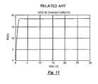
- Fig. 11 shows the drain current ID, which is a main current with respect to the voltage VDS between the source and drain of the output MOSFET 101 in this status.
- the detection current that flows through the detection MOSFET 104 increases, and detection voltage, based on the drop in voltage of the detection resistor 105, also increases. And if the detection voltage exceeds the threshold voltage of the over-current protection MOSFET 106, the MOSFET 106 turns ON and the input to the output MOSFET 101 is divided by the gate resistor 103 and the over-current protection MOSFET 106, so the potential at the potential point A dramatically drops.
- the potential at the potential point A drops, the main current of the output MOSFET 101 and the detection current of the detection MOSFET 104 also decrease as the gate voltage drops, and a breakdown of the output MOSFET 101 by the over-current is prevented. In this case, the potential of the potential point A drops according to the magnitude of the detection voltage to be applied to the gate of the over-current protection MOSFET 106.
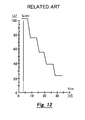
- FIG. 12 shows the current limiting characteristics of a conventional semiconductor device stated in "Smart Highside Power Switch", Data sheet BTS 6143D, p.13, Figure 3a, Infineon Technologies AG in Germany, October 1, 2003, which is disclosed on internet and found by searching on February 17, 2004 at URL: http://www.infineon.com/cmc_upload/documents/014/444/BTS6143D _20030925.pdf.
- a double diffusion type field effect transistor composed of cells shown in Fig. 13 and Fig. 14, is normally used for the output MOSFET 101 and the detection MOSFET 104 shown in Fig. 10.
- Fig. 13 is a plain view of a vertical MOSFET and
- Fig. 14 is a cross-sectional view along the XIV-XIV line in Fig. 13.
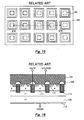
- This vertical MOSFET has a structure where a plurality of unit cells, in which one source electrode 107 is surrounded by the gate electrode 108, and an epitaxial layer 110 having low density n-type impurities (n-) is formed on a semiconductor substrate 109 having high density n-type impurities (n+), and using these as a drain area, a double diffusion area which is composed of a base area 111 having p-type impurities and a source area 112 having high density n-type impurities is formed in the epitaxial layer 110, and the gate electrode 108, source electrode 107 and drain electrode 113 are formed respectively, as shown in Fig. 14.
- Fig. 15 is a plain view of a conventional semiconductor device
- Fig. 16 is a cross-sectional view along the XVI-XVI line in Fig. 15.
- This conventional semiconductor device is a semiconductor device with a trench structure where the gate electrode 108 is buried in the base area 111 and epitaxial layer 110.
- a merit of using a double diffusion type field effect transistor of which the ON resistance per unit area is low is that the size of the output MOSFET can be decreased.
- the conventional semiconductor device shown in Fig. 10 has the following problem. That is, unless the current limit value is decreased for the amount of the decreased size of the output MOSFET, the heating value when such an abnormality as a load short circuit occurs increases, which makes it easier for the semiconductor device to breakdown, and if the current limit value is decreased, the semiconductor device cannot be used for high output applications where large current flows.
- the current limit value is increased in an area where voltage is low, that is a safe operation area, and the current limit value is decreased in an area where voltage is high, that is outside the safe operation area.
- the structure of the technique disclosed in “Smart Highside Power Switch” requires a voltage detection circuit and a circuit to change the current limit value for each stage, so the circuit scale is about five times larger than the semiconductor device in Fig. 10, which is the downside of this approach.
- a semiconductor device comprising an output transistor for controlling current that flows between a first terminal and a second terminal, a detection transistor connected in parallel with the output transistor, a detection resistor connected in series with the detection transistor, for detecting current that flows through the detection transistor as detection voltage and of which the resistance value is set in proportion to the potential difference between the first terminal and the second terminal and an over-current protection transistor for decreasing the ON current of the output transistor and the detection transistor according to the increase of the detection voltage.
- a semiconductor device comprising a drive circuit for controlling drive current that flows through a load, a detection resistor to which detection current for detecting the drive current is supplied and of which the resistance value changes based on a predetermined potential of the drive circuit on a route where the drive current flows and a control circuit for controlling the drive status of the drive circuit based on the voltage of the detection resistor.
- a semiconductor device comprising an output transistor of which drain is connected to a first power supply via a load and source is connected to a second power supply, a detection transistor of which drain is connected to the drain of said output transistor and gate is connected to the gate of the output transistor, a detection resistor of which one end is connected to the source of the detection transistor and the other end is connected to the source of the output transistor, and of which resistance value changes based on the drain voltage of the output transistor and an over-current protection transistor of which drain is connected to the gate of the output transistor, source is connected to the source of the output transistor, and gate is connected to the source of the detection transistor.
- the resistance value of the detection resistor increases and the current of the output transistor (drain current) decreases as the voltage of the output transistor (drain voltage) increases. Therefore the flow of over-current is limited and power consumption can be deceased when load is abnormal, and the semiconductor device can be protected from breakdown. Also it is not necessary to dispose a plurality of over-current detection circuits and current control circuits, therefore the circuit scale and the area of the semiconductor chip can be decreased.
- Fig. 1 is a circuit diagram showing the configuration of the semiconductor device according to the first embodiment of the present invention.
- This semiconductor device comprises a detection resistor 5 of which the resistance value changes depending on the drain voltage, instead of the detection resistor 105, which has a fixed resistance value, of the conventional art in Fig. 10.
- the output MOSFET 1, detection MOSFET 4 and detection resistor 5 in Fig. 1 are formed on a same semiconductor substrate, and the output MOSFET 1 and detection MOSFET 4 have a vertical double diffusion type field effect transistor structure composed of the cell configuration in Fig. 13 and Fig. 14, or a structure burying the gate electrode 107 in Fig. 15 and Fig. 16 as a structure where the ON resistance is smaller.
- Components other than the detection resistor 5 are formed in a conventional structure by a conventional manufacturing method.
- the semiconductor device has the output MOSFET 1 constituting the main current switch.
- the drain of the output MOSFET 1 is connected to the first terminal 7 and the source is connected to the second terminal 8.
- the semiconductor device also has a current limiting circuit comprising the detection MOSFET 4, detection resistor 5 and over-current protection MOSFET 6.
- the detection MOSFET 4 is connected with the output MOSFET 1 in parallel, the drain is connected to the first terminal 7, the gate is connected with the gate of the output MOSFET 1 at the potential point A and is connected to the control terminal 2 via the gate resistor 3, and the source is connected to one terminal of the detection resistor 5 and the gate of the over-current protection MOSFET 6.
- the output MOSFET 1 is a drive circuit for controlling drive current that flows through the load circuit 16.
- the detection resistor 5 is a resistor to which detection current for detecting the drive current is supplied and of which the resistance value changes based on a predetermined potential (the potential of the first terminal 7) of the output MOSFET 1 on a route where the drive current flows.
- the over-current protection MOSFET 6 is a control circuit for controlling the drive status of the output MOSFET 1 based on the voltage of the detection resistor 5.
- Fig. 2 is a plain view of the detection resistor 5 in Fig. 1
- Fig. 3 and Fig. 4 are cross-sectional views along the III-III line and the IV-IV line respectively in Fig. 2.
- the epitaxial layer 10 having low density n-type impurities is formed on the semiconductor substrate 9 having high density n-type impurities.
- the semiconductor substrate 9 and the epitaxial layer 10 become a part of the drain area of the output MOSFET 1.
- the semiconductor layer 11 having low density p-type impurities and the contact layers 12a and 12b having p-type impurities are formed in the epitaxial layer 10, and the insulation film 13 including an oxide film is formed on these layers and the epitaxial layer 10, and the electrodes 14a and 14b which are electrically connected with the contact layers 12a and 12b are formed on the contact layers 12a and 12b.
- the semiconductor layer 11 is a first semiconductor layer.
- a combination of the semiconductor substrate 9 and the epitaxial layer 10 is a second semiconductor layer.
- the electrodes 14a and 14b are connected to the source electrode of the output MOSFET 1 and source electrode of detection MOSFET 4 respectively. A drain voltage is applied from the bottom to the semiconductor substrate 9.
- the same voltage as the voltage VDS between the drain and source of the output MOSFET 1 is applied to the detection resistor 5. Therefore if the drain voltage is increased, the amount of electric charges to flow decreases since the depletion layer where many carries do not exist, spread in the semiconductor layer 11, and the resistance value of the semiconductor layer 11 increases.
- the first terminal 7 of the semiconductor device is connected to the power supply 17 via the load circuit 16, and the second terminal 8 is grounded.
- this gate voltage is applied to the gates of the output MOSFET 1 and the detection MOSFET 4 via the gate resistor 3, and main current flows through the first terminal 7 which is the drain of the output MOSFET 1 and the second terminal 7 which is the source thereof, and detection current flows through the detection MOSFET 4 at the same time.
- the detection current is set to a value about 1/1000 - 1/10000 of the main current.
- the detection current flows through the detection resistor 5 which is connected to the detection MOSFET 4 in series, and detection voltage is detected by the drop in voltage generated in the detection resistor 5.
- the over-current protection MOSFET 6 turns ON and is shorted via the ON resistor of the over-current protection MOSFET 6, and gate voltage at the potential point A drops dramatically. This gate voltage drops according to the magnitude of the detection voltage to be applied to the gate of the over-current protection MOSFET 6. If the gate voltage at the potential point A drops, the main current of the output MOSFET 1 and the current of the detection MOSFET 4 also decrease according to the drop in the gate voltage.
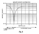
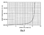
- the drain voltage to be applied to the detection resistor 5 is 16.5V
- the entire semiconductor layer 11 is depleted
- the resistance value of the detection resistor 5 becomes infinite.
- the sheet resistance of the semiconductor layer 11, with respect to the drain voltage becomes the value shown in Fig. 6.
- the drain current characteristic, with respect to the drain - source voltage VDS of the output MOSFET 1 becomes as shown in Fig. 7, where as the drain - source voltage VDS of the output MOSFET 1 increases, the drain current ID decreases, and the drain current ID stops flowing at voltage 16.5V at which the entire semiconductor 11 is depleted.
- the voltage at which the drain current ID stops flowing can be changed by the impurity density and the depth of the junctions of the semiconductor layer 11, but must be set to a value that is higher than the load drive voltage.
- the configuration of the present invention with which the drain current ID that can flow is limited and decreased if the drain voltage rises, can decrease the power consumption when such an abnormality as a load short circuit occurs, and prevent the semiconductor device from breakdown, and also increase the current limit value in an area where voltage is low, which is a safe operation area, so a semiconductor device which can be used for high current can be implemented using a current limiting circuit with a small circuit scale.
- the manufacturing method for the detection resistor portion of the semiconductor device according to the first embodiment will be described with reference to Fig. 3.
- the epitaxial layer 10 having low density n-type impurities is formed by epitaxial growth as a drain area of the output MOSFET 1 on the semiconductor substrate 9 having high density n-type impurities.
- boron ions at a 12 to 13 power order per 1 cm 2 are implanted into a partial area of this epitaxial layer 10 by an ion implanter, then thermal processing is performed for several hours at a 1100 - 1200 °C temperature to form a semiconductor layer 11 having low density p-type impurities.
- contact layers 12a and 12b having p-type impurities are formed so as to be connected to opposite ends of the semiconductor layer 11 respectively.
- an insulation film 13 including oxide film is formed on the surface.
- the insulation film at the center part of the contact layers 12a and 12b is removed, and the electrodes 14a and 14b made of aluminum are formed, and a semiconductor device having a detection resistor 5, of which the resistance value changes depending on the drain voltage of the output MOSFET 1, is created.
- Fig. 8 is a circuit diagram showing the configuration of the semiconductor device according to the second embodiment of the present invention, where composing elements the same as the first embodiment in Fig. 1 are denoted with the same reference symbols.
- the difference from the first embodiment is that a resistor 15 having a fixed resistance value is connected in parallel to the detection resistor 5.
- the resistance value between the source of the output MOSFET 1 and the source of the detection MOSFET 4 does not become infinite even if the drain current ID according to the fixed resistance value of the resistor 15 flows, and the drain voltage of the detection resistor 5 becomes a value with which the entire semiconductor layer 11 is depleted.
- a MOSFET was described as an example of a transistor, but this is not limited to MOSFET, since a similar effect can be exhibited merely if the transistor is one of which the ON current is controlled according to the control voltage, such as an insulation gate bi-polar transistor.
Landscapes
- Metal-Oxide And Bipolar Metal-Oxide Semiconductor Integrated Circuits (AREA)
- Semiconductor Integrated Circuits (AREA)
- Logic Circuits (AREA)
- Electronic Switches (AREA)
Applications Claiming Priority (2)
| Application Number | Priority Date | Filing Date | Title |
|---|---|---|---|
| JP2004070536A JP2005260658A (ja) | 2004-03-12 | 2004-03-12 | 半導体装置 |
| JP2004070536 | 2004-03-12 |
Publications (1)
| Publication Number | Publication Date |
|---|---|
| EP1575168A2 true EP1575168A2 (de) | 2005-09-14 |
Family
ID=34824623
Family Applications (1)
| Application Number | Title | Priority Date | Filing Date |
|---|---|---|---|
| EP05002820A Withdrawn EP1575168A2 (de) | 2004-03-12 | 2005-02-10 | Halbleiterschaltung |
Country Status (4)
| Country | Link |
|---|---|
| US (1) | US7259951B2 (de) |
| EP (1) | EP1575168A2 (de) |
| JP (1) | JP2005260658A (de) |
| CN (1) | CN100442193C (de) |
Families Citing this family (15)
| Publication number | Priority date | Publication date | Assignee | Title |
|---|---|---|---|---|
| JP5022668B2 (ja) * | 2006-10-25 | 2012-09-12 | オンセミコンダクター・トレーディング・リミテッド | Dc/dcコンバータ |
| US7672102B2 (en) * | 2006-12-31 | 2010-03-02 | Texas Instruments Incorporated | Electrical overstress protection |
| JP2008235856A (ja) * | 2007-02-22 | 2008-10-02 | Matsushita Electric Ind Co Ltd | 半導体装置 |
| JP5129701B2 (ja) * | 2008-09-12 | 2013-01-30 | ルネサスエレクトロニクス株式会社 | 過電流検出回路 |
| JP5352500B2 (ja) | 2010-03-02 | 2013-11-27 | ルネサスエレクトロニクス株式会社 | 半導体装置 |
| JP5811803B2 (ja) * | 2011-11-22 | 2015-11-11 | 住友電気工業株式会社 | 半導体装置及び半導体装置の製造方法 |
| CN104124742B (zh) * | 2013-04-26 | 2016-05-18 | 立锜科技股份有限公司 | 电源供应控制方法 |
| JP6520102B2 (ja) * | 2014-12-17 | 2019-05-29 | 富士電機株式会社 | 半導体装置および電流制限方法 |
| US10079599B2 (en) * | 2016-10-14 | 2018-09-18 | Infineon Technologies Ag | Controlling at least two transistors |
| JP6983527B2 (ja) * | 2017-03-30 | 2021-12-17 | Koa株式会社 | 電流検出用抵抗器 |
| FR3082052B1 (fr) * | 2018-06-04 | 2020-06-26 | Stmicroelectronics Sa | Dispositif electronique integre destine a fonctionner dans des environnements a temperature variable |
| CN111371080B (zh) * | 2018-12-25 | 2022-08-30 | 上海睿驱微电子科技有限公司 | 一种具有过流限制功能的设备及其构建方法 |
| US11362504B2 (en) * | 2020-07-20 | 2022-06-14 | Analog Devices International Unlimited Company | Over current sensing scheme for switch applications |
| CN112531650A (zh) * | 2020-12-07 | 2021-03-19 | 华羿微电子股份有限公司 | 一种自带短路保护的功率mosfet |
| CN116760400B (zh) * | 2023-08-16 | 2023-11-07 | 青岛嘉展力芯半导体有限责任公司 | 串叠结构及电子装置 |
Family Cites Families (9)
| Publication number | Priority date | Publication date | Assignee | Title |
|---|---|---|---|---|
| US4553084A (en) * | 1984-04-02 | 1985-11-12 | Motorola, Inc. | Current sensing circuit |
| US4893158A (en) * | 1987-06-22 | 1990-01-09 | Nissan Motor Co., Ltd. | MOSFET device |
| US5115188A (en) * | 1987-07-16 | 1992-05-19 | Peter Norton | Resistance sensor and switch |
| JPH07113861B2 (ja) * | 1988-01-29 | 1995-12-06 | 株式会社日立製作所 | 半導体素子の状態検出及び保護回路とそれを用いたインバータ回路 |
| DE69311921T2 (de) * | 1992-02-03 | 1998-01-29 | Philips Electronics Nv | Anordnung zum Ein- und Ausschalten eines Leistungstransistors |
| JPH07146722A (ja) * | 1993-10-01 | 1995-06-06 | Fuji Electric Co Ltd | トランジスタ用過電流保護装置 |
| JPH1014099A (ja) * | 1996-06-21 | 1998-01-16 | Nec Corp | 過電流検出回路 |
| JP2001282372A (ja) * | 2000-03-31 | 2001-10-12 | Seiko Instruments Inc | レギュレータ |
| JP3610556B1 (ja) * | 2003-10-21 | 2005-01-12 | ローム株式会社 | 定電圧電源装置 |
-
2004
- 2004-03-12 JP JP2004070536A patent/JP2005260658A/ja active Pending
-
2005
- 2005-02-10 EP EP05002820A patent/EP1575168A2/de not_active Withdrawn
- 2005-03-10 US US11/075,861 patent/US7259951B2/en not_active Expired - Fee Related
- 2005-03-14 CN CNB2005100527754A patent/CN100442193C/zh not_active Expired - Fee Related
Also Published As
| Publication number | Publication date |
|---|---|
| US20050200398A1 (en) | 2005-09-15 |
| CN1667540A (zh) | 2005-09-14 |
| JP2005260658A (ja) | 2005-09-22 |
| US7259951B2 (en) | 2007-08-21 |
| CN100442193C (zh) | 2008-12-10 |
Similar Documents
| Publication | Publication Date | Title |
|---|---|---|
| US7259951B2 (en) | Semiconductor device | |
| US6804159B2 (en) | Semiconductor device having fuse and its manufacture method | |
| CN103178059B (zh) | 功率集成电路器件 | |
| JP5585593B2 (ja) | 半導体装置 | |
| TW285768B (de) | ||
| EP2187441A1 (de) | Schaltvorrichtung für einen elektrischen schaltkreis | |
| US8143673B1 (en) | Circuit with electrostatic discharge protection | |
| JP4960540B2 (ja) | 半導体装置 | |
| US5500547A (en) | Integrated semiconductor device with temperature sensing circuit and method for operating same | |
| US7187034B2 (en) | Distributed power MOSFET | |
| JP2006032543A (ja) | 半導体集積回路装置 | |
| US20050285200A1 (en) | Device for electrostatic discharge protection | |
| US5821586A (en) | Semiconductor device including a protective element having negative resistance characteristic | |
| US20180240792A1 (en) | Semiconductor device | |
| EP0580242A1 (de) | Halbleiterbauelement mit einem Schutzmittel | |
| US8148785B2 (en) | Semiconductor device | |
| US10490656B2 (en) | Charge-compensation semiconductor device and a manufacturing method therefor | |
| EP4369414A2 (de) | Transistor mit integriertem kurzschlussschutz | |
| JP4547790B2 (ja) | 半導体装置 | |
| JP2004031980A (ja) | 複合型mosfet | |
| JP5267510B2 (ja) | 半導体装置 | |
| US8217460B2 (en) | Semiconductor device with electrostatic protection device | |
| JP2009124085A (ja) | 半導体装置 | |
| TW202404023A (zh) | 具有多對pn條帶之靜電放電保護裝置及其製造方法 | |
| JP2007258346A (ja) | 半導体装置 |
Legal Events
| Date | Code | Title | Description |
|---|---|---|---|
| PUAI | Public reference made under article 153(3) epc to a published international application that has entered the european phase |
Free format text: ORIGINAL CODE: 0009012 |
|
| AK | Designated contracting states |
Kind code of ref document: A2 Designated state(s): AT BE BG CH CY CZ DE DK EE ES FI FR GB GR HU IE IS IT LI LT LU MC NL PL PT RO SE SI SK TR |
|
| AX | Request for extension of the european patent |
Extension state: AL BA HR LV MK YU |
|
| STAA | Information on the status of an ep patent application or granted ep patent |
Free format text: STATUS: THE APPLICATION HAS BEEN WITHDRAWN |
|
| 18W | Application withdrawn |
Effective date: 20051010 |