EP1566883A2 - Oscillateur LC - Google Patents
Oscillateur LC Download PDFInfo
- Publication number
- EP1566883A2 EP1566883A2 EP05103450A EP05103450A EP1566883A2 EP 1566883 A2 EP1566883 A2 EP 1566883A2 EP 05103450 A EP05103450 A EP 05103450A EP 05103450 A EP05103450 A EP 05103450A EP 1566883 A2 EP1566883 A2 EP 1566883A2
- Authority
- EP
- European Patent Office
- Prior art keywords
- conductor
- inductor
- substrate
- oscillator
- conductors
- Prior art date
- Legal status (The legal status is an assumption and is not a legal conclusion. Google has not performed a legal analysis and makes no representation as to the accuracy of the status listed.)
- Withdrawn
Links
Images






Classifications
-
- H—ELECTRICITY
- H03—ELECTRONIC CIRCUITRY
- H03B—GENERATION OF OSCILLATIONS, DIRECTLY OR BY FREQUENCY-CHANGING, BY CIRCUITS EMPLOYING ACTIVE ELEMENTS WHICH OPERATE IN A NON-SWITCHING MANNER; GENERATION OF NOISE BY SUCH CIRCUITS
- H03B5/00—Generation of oscillations using amplifier with regenerative feedback from output to input
- H03B5/18—Generation of oscillations using amplifier with regenerative feedback from output to input with frequency-determining element comprising distributed inductance and capacitance
- H03B5/1841—Generation of oscillations using amplifier with regenerative feedback from output to input with frequency-determining element comprising distributed inductance and capacitance the frequency-determining element being a strip line resonator
-
- H—ELECTRICITY
- H01—ELECTRIC ELEMENTS
- H01F—MAGNETS; INDUCTANCES; TRANSFORMERS; SELECTION OF MATERIALS FOR THEIR MAGNETIC PROPERTIES
- H01F17/00—Fixed inductances of the signal type
- H01F17/0006—Printed inductances
-
- H—ELECTRICITY
- H03—ELECTRONIC CIRCUITRY
- H03B—GENERATION OF OSCILLATIONS, DIRECTLY OR BY FREQUENCY-CHANGING, BY CIRCUITS EMPLOYING ACTIVE ELEMENTS WHICH OPERATE IN A NON-SWITCHING MANNER; GENERATION OF NOISE BY SUCH CIRCUITS
- H03B5/00—Generation of oscillations using amplifier with regenerative feedback from output to input
- H03B5/08—Generation of oscillations using amplifier with regenerative feedback from output to input with frequency-determining element comprising lumped inductance and capacitance
- H03B5/12—Generation of oscillations using amplifier with regenerative feedback from output to input with frequency-determining element comprising lumped inductance and capacitance active element in amplifier being semiconductor device
- H03B5/1203—Generation of oscillations using amplifier with regenerative feedback from output to input with frequency-determining element comprising lumped inductance and capacitance active element in amplifier being semiconductor device the amplifier being a single transistor
-
- H—ELECTRICITY
- H03—ELECTRONIC CIRCUITRY
- H03B—GENERATION OF OSCILLATIONS, DIRECTLY OR BY FREQUENCY-CHANGING, BY CIRCUITS EMPLOYING ACTIVE ELEMENTS WHICH OPERATE IN A NON-SWITCHING MANNER; GENERATION OF NOISE BY SUCH CIRCUITS
- H03B5/00—Generation of oscillations using amplifier with regenerative feedback from output to input
- H03B5/08—Generation of oscillations using amplifier with regenerative feedback from output to input with frequency-determining element comprising lumped inductance and capacitance
- H03B5/12—Generation of oscillations using amplifier with regenerative feedback from output to input with frequency-determining element comprising lumped inductance and capacitance active element in amplifier being semiconductor device
- H03B5/1231—Generation of oscillations using amplifier with regenerative feedback from output to input with frequency-determining element comprising lumped inductance and capacitance active element in amplifier being semiconductor device the amplifier comprising one or more bipolar transistors
-
- H—ELECTRICITY
- H03—ELECTRONIC CIRCUITRY
- H03B—GENERATION OF OSCILLATIONS, DIRECTLY OR BY FREQUENCY-CHANGING, BY CIRCUITS EMPLOYING ACTIVE ELEMENTS WHICH OPERATE IN A NON-SWITCHING MANNER; GENERATION OF NOISE BY SUCH CIRCUITS
- H03B5/00—Generation of oscillations using amplifier with regenerative feedback from output to input
- H03B5/08—Generation of oscillations using amplifier with regenerative feedback from output to input with frequency-determining element comprising lumped inductance and capacitance
- H03B5/12—Generation of oscillations using amplifier with regenerative feedback from output to input with frequency-determining element comprising lumped inductance and capacitance active element in amplifier being semiconductor device
- H03B5/1237—Generation of oscillations using amplifier with regenerative feedback from output to input with frequency-determining element comprising lumped inductance and capacitance active element in amplifier being semiconductor device comprising means for varying the frequency of the generator
- H03B5/124—Generation of oscillations using amplifier with regenerative feedback from output to input with frequency-determining element comprising lumped inductance and capacitance active element in amplifier being semiconductor device comprising means for varying the frequency of the generator the means comprising a voltage dependent capacitance
- H03B5/1243—Generation of oscillations using amplifier with regenerative feedback from output to input with frequency-determining element comprising lumped inductance and capacitance active element in amplifier being semiconductor device comprising means for varying the frequency of the generator the means comprising a voltage dependent capacitance the means comprising voltage variable capacitance diodes
-
- H—ELECTRICITY
- H10—SEMICONDUCTOR DEVICES; ELECTRIC SOLID-STATE DEVICES NOT OTHERWISE PROVIDED FOR
- H10W—GENERIC PACKAGES, INTERCONNECTIONS, CONNECTORS OR OTHER CONSTRUCTIONAL DETAILS OF DEVICES COVERED BY CLASS H10
- H10W20/00—Interconnections in chips, wafers or substrates
- H10W20/40—Interconnections external to wafers or substrates, e.g. back-end-of-line [BEOL] metallisations or vias connecting to gate electrodes
-
- H—ELECTRICITY
- H10—SEMICONDUCTOR DEVICES; ELECTRIC SOLID-STATE DEVICES NOT OTHERWISE PROVIDED FOR
- H10W—GENERIC PACKAGES, INTERCONNECTIONS, CONNECTORS OR OTHER CONSTRUCTIONAL DETAILS OF DEVICES COVERED BY CLASS H10
- H10W20/00—Interconnections in chips, wafers or substrates
- H10W20/40—Interconnections external to wafers or substrates, e.g. back-end-of-line [BEOL] metallisations or vias connecting to gate electrodes
- H10W20/497—Inductive arrangements or effects of, or between, wiring layers
-
- H—ELECTRICITY
- H01—ELECTRIC ELEMENTS
- H01F—MAGNETS; INDUCTANCES; TRANSFORMERS; SELECTION OF MATERIALS FOR THEIR MAGNETIC PROPERTIES
- H01F17/00—Fixed inductances of the signal type
- H01F17/0006—Printed inductances
- H01F17/0013—Printed inductances with stacked layers
-
- H—ELECTRICITY
- H01—ELECTRIC ELEMENTS
- H01F—MAGNETS; INDUCTANCES; TRANSFORMERS; SELECTION OF MATERIALS FOR THEIR MAGNETIC PROPERTIES
- H01F17/00—Fixed inductances of the signal type
- H01F17/0006—Printed inductances
- H01F2017/0046—Printed inductances with a conductive path having a bridge
-
- H—ELECTRICITY
- H01—ELECTRIC ELEMENTS
- H01F—MAGNETS; INDUCTANCES; TRANSFORMERS; SELECTION OF MATERIALS FOR THEIR MAGNETIC PROPERTIES
- H01F27/00—Details of transformers or inductances, in general
- H01F27/34—Special means for preventing or reducing unwanted electric or magnetic effects, e.g. no-load losses, reactive currents, harmonics, oscillations, leakage fields
-
- H—ELECTRICITY
- H01—ELECTRIC ELEMENTS
- H01F—MAGNETS; INDUCTANCES; TRANSFORMERS; SELECTION OF MATERIALS FOR THEIR MAGNETIC PROPERTIES
- H01F27/00—Details of transformers or inductances, in general
- H01F27/34—Special means for preventing or reducing unwanted electric or magnetic effects, e.g. no-load losses, reactive currents, harmonics, oscillations, leakage fields
- H01F27/38—Auxiliary core members; Auxiliary coils or windings
-
- H—ELECTRICITY
- H03—ELECTRONIC CIRCUITRY
- H03B—GENERATION OF OSCILLATIONS, DIRECTLY OR BY FREQUENCY-CHANGING, BY CIRCUITS EMPLOYING ACTIVE ELEMENTS WHICH OPERATE IN A NON-SWITCHING MANNER; GENERATION OF NOISE BY SUCH CIRCUITS
- H03B2201/00—Aspects of oscillators relating to varying the frequency of the oscillations
- H03B2201/02—Varying the frequency of the oscillations by electronic means
- H03B2201/0208—Varying the frequency of the oscillations by electronic means the means being an element with a variable capacitance, e.g. capacitance diode
Definitions
- the present invention relates to an LC oscillator that can be formed on various kinds of substrates such as a semiconductor substrate.
- the present invention is achieved in view of such a point. Its object is to provide an LC oscillator that can perform oscillation even if the LC oscillator is formed on a substrate.
- An inductor element included in an LC oscillator of the present invention has two conductors that are formed in piles on a substrate in the state where they are mutually insulated, and are connected with each other at both odd ends. While one conductor separating from the substrate is used as an inductor conductor, a lead wire of this inductor conductor is led out through a gap between another conductor, being near the substrate, and the substrate. It is experimentally confirmed that an inductor element that has such structure has predetermined inductance without losing an inductance component by eddy currents etc. even if the inductor element is formed on a substrate.
- this inductor element as a part of an LC oscillator, oscillation can be performed even if the LC oscillator is formed on the substrate.
- this inductor conductor included in the inductor element by leading out the lead wire of this inductor conductor included in the inductor element from between another conductor and the substrate, it becomes possible to preventing the flow of the effective magnetic flux, generated by the inductor conductor, to the minimum from being interrupted. Hence good characteristics can be obtained.
- the inductor element described above has three or more layers of metal layers formed on the substrate, it is desirable to form the two conductors described above and lead wires respectively with using different metal layers which are mutually apart by one or more layers. Since the inductor conductor can be made to be apart from the lead wires by at least two or more layers by adopting such constitution of the inductor element included in the LC oscillator, it is possible to further reduce the influence of the electric current that flows in the lead wires.
- an inductor element included in the LC oscillator of the present invention has two conductors that are formed in piles on a substrate in the state where they are mutually insulated, and are connected with each other at both odd ends. While using one conductor apart from the substrate as an inductor conductor, one end of another conductor not connected to the inductor conductor is terminated with a predetermined impedance element. Although electric current flows also in another conductor by the effective magnetic flux generated by the inductor conductor in the inductor element, it becomes possible to prevent unnecessary reflection in this portion and to improve characteristics of the inductor element by terminating the end of the free side of another conductor with the impedance element.
- oscillation can be performed reliably by the LC oscillator comprising the inductor element.
- it is possible to adjust frequency characteristics or the like of another conductor by forming the impedance element described above with using any of a resistor, a capacitor, and an inductor or combining these.
- termination conditions by making it possible to change at least one device constant of a resistor, a capacitor, and an inductor, which constitute the impedance element described above, and making this device constant variable.
- a device constant of the whole impedance element that is, characteristics of the inductor element by a change of termination conditions. It also becomes possible to adjust finely an oscillation frequency.
- the substrate described above is a semiconductor substrate
- the substrate described above is a semiconductor substrate, it is desirable to form a variable resister made of an FET whose channel is used as a resistor.
- variable resistor made of the FET formed with using the semiconductor substrate it becomes possible to reduce a cost for manufacturing LC oscillator by simplifying manufacturing process in comparison with the case where external parts are attached thereafter, and wiring etc. are performed.
- an inductor which constitutes the impedance element, by a conductive layer formed on the substrate in predetermined shape. Since high Q is not required of the inductor used for terminating one end of a conductor, it is possible to realize the inductor with a conductor pattern on the substrate. Moreover, since it becomes possible to form this conductor pattern at the same process with using a metal layer for performing various kinds of wiring etc., it becomes possible to perform miniaturization of entire LC oscillator, simplification of process, and cost reduction.
- each configuration parts of LC oscillator it is preferable to use a semiconductor substrate, and to form each configuration parts of LC oscillator on the substrate. If the inductor element that effectively functions can be formed on a semiconductor substrate, it is possible to form each configuration parts for LC oscillator, including the inductor element, on the semiconductor substrate. Hence it becomes possible to form the whole of the LC oscillator on the semiconductor substrate without using any external parts.
- the conductor is desirable to form two conductors, described above, in the substantially same shape or long shape. Since an upper conductor never directly faces the front side of the substrate owing to making the two conductors the same in shapes, it is possible to reduce the eddy currents that are generated on the substrate when the upper conductor directly faces the substrate. In addition, it is possible to give predetermined inductance to the upper conductor by making the shapes of the two conductors be long. In particular, since it is possible to give large inductance to a conductor when the conductor is formed in one or more turns of spiral shape or a meander shape, the conductor is suitable for being built in an LC oscillator having comparatively low frequency.
- the conductor is suitable for being built in an LC oscillator having comparatively high frequency.
- the inductor element described above is suitable for use as a compound element that also has a capacitance component besides an inductance component. Since this inductor element has two conductors, mutually superimposed, and a capacitance component is also included in its characteristics, the characteristics of this inductor element can be effectively used by using this inductor element as one part of the LC oscillator where an inductor and a capacitor are used in combination.
- a LC oscillator uses an inductor element formed on a substrate, whereby the inductor element has two conductors that are formed in piles on the substrate in the state where they are mutually insulated, and are mutually connected at both odd ends, and whereby one of the conductors apart from the substrate is used as an inductor conductor, and further, an end that is an end of another one of the conductors and is not connected to the inductor conductor is terminated with a predetermined impedance element.
- the substrate is a semiconductor substrate
- the capacitor is formed of a variable capacitance diode made of a semiconductor layer formed in the inside or outside of the semiconductor substrate.
- the resistor is formed of a channel of an FET made of a semiconductor layer formed in the inside or outside of the semiconductor substrate. It is also possible that the components are formed on the substrate in which the inductor element is formed.
- the two conductors have substantially the same shape and, in particular, they have long shapes, and one end of one conductor in a longitudinal direction is connected with one end of the other in the longitudinal direction.
- the two conductors can also have circular shapes less than one turn, and one end of one conductor is connected with one end of the other.
- the two conductors can have spiral shapes each number of turns of which is one or more, and one end of one conductor is connected with one end of the other.
- the two conductors may be formed in substantially linear shapes, and one end of one conductor is connected with one end of the other.
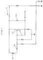
- FIG. 1 is a circuit diagram showing a configuration of an LC oscillator according to a first embodiment
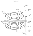
- FIG. 2 is a schematic diagram showing a planar structure of an inductor element included in the LC oscillator shown in FIG. 1;
- FIG. 3 is a drawing showing an upper layer of conductor included in the inductor element shown in FIG. 2;
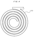
- FIG. 4 is a drawing showing a shape of a lower layer of conductor included in the inductor element shown in FIG. 2;
- FIG. 5 is a schematic diagram showing a connection state of two conductors included in an inductor conductor
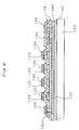
- FIG. 6 is an enlarged sectional view taken on line VI-VI in FIG. 2;
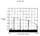
- FIG. 7 is a chart showing measurement result of an output characteristic of an LC oscillator
- FIG. 8 is a chart showing measurement result of an output characteristic of an LC oscillator
- FIG. 9 is a chart showing measurement result of an output characteristic of an LC oscillator
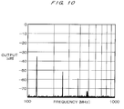
- FIG. 10 is a chart showing measurement result of an output characteristic of an LC oscillator
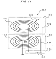
- FIG. 11 is a schematic diagram showing a structure of an inductor element according to a second embodiment
- FIG. 12 is a drawing showing the structure in the case of connecting a variable capacitance diode to the inner circumferential end of a lower layer of conductor;
- FIG. 13 is a drawing showing the cross-sectional structure in the case of forming the variable capacitance diode, shown in FIG. 12, on a semiconductor substrate;
- FIG. 14 is a diagram showing the structure in the case of connecting a variable resistor to the inner circumferential end of a lower layer of conductor;
- FIG. 15 is a chart showing measurement result of an output characteristic of an LC oscillator
- FIG. 16 is a chart showing measurement result of an output characteristic of an LC oscillator
- FIGs. 17A through 17C are schematic diagrams showing modified examples of the conductors included in the inductor elements.
- FIG. 18 is a drawing showing a modified example of the inductor element, the drawing where a connecting wire that connects ends of two conductors is omitted.
- FIG. 1 is a circuit diagram showing a configuration of an LC oscillator according to the first embodiment.
- An LC oscillator 10 shown in FIG. 1 has a transistor 20, a capacitor 22 connected between the base and the emitter of the transistor 20, a capacitor 24 connected between the emitter and the collector of the transistor 20, a capacitor 26 connected serially between the base and the collector of the transistor 20 and an inductor element 30.
- the capacitance of two capacitors 22 and 24 may be several tens times the between-terminal capacity of a transistor 20.
- an inductor element 30 is connected through a capacitor 26.
- An LC oscillator 10 having the configuration described above in this embodiment is a Clapp circuit that is an advanced Colpitts circuit.
- a capacitor of a resonant circuit that determines an oscillation frequency becomes equivalent to series connection of capacitors 22, 24, and 26.
- FIG. 2 is a schematic diagram showing a planar structure of an inductor element 30 included in the LC oscillator 10 according to this embodiment.
- FIG. 3 is a drawing showing an upper layer of conductor included in the inductor element 30 shown in FIG. 2.
- FIG. 4 is a drawing showing a shape of a lower layer of conductor included in the inductor element 30 shown in FIG. 2.
- An inductor element 30 has two conductors 120 and 122 that have spiral shapes and are formed on the surface of a semiconductor substrate 110. These two conductors 120 and 122 have substantially the same shape. When viewed from the front side of the semiconductor substrate 110, they are formed so that the conductor 120, which becomes an upper layer, and another conductor 122, which becomes a lower layer, are formed by being superimposed one on the other substantially exactly.
- Each of the conductors 120 and 122 is formed of, for examples, a thin film of metal (metal layer), or semiconductor material such as poly silicon.
- FIG. 5 is a schematic diagram showing a connection state of the two conductors 120 and 122, described above.
- lead wires 130 and 132 are connected to an outer end (outer circumferential end) and an inner end (inner circumferential end) of the upper conductor 120 respectively, and the inner end of the upper conductor 120 and the outer end of the lower conductor 122 are connected with a connecting wire 134.
- the upper conductor 120 functions as an inductor conductor, and is connected to other configuration parts formed on the semiconductor substrate 110 through the lead wires 130 and 132 connected to ends thereof.
- FIG. 6 is an enlarged sectional view taken on line VI-VI in FIG. 2. As shown in FIGS. 5 and 6, at least three layers of metal layers 160, 162, and 164 are formed on the surface of the semiconductor substrate 110.
- One conductor 120 as an inductor conductor is formed with using a top layer of metal layer 160 that is most apart from the semiconductor substrate 110, and another conductor 122 is formed with using a middle layer of metal layer 162.
- the lead wire 132 led out from the inner circumferential end of the top layer of conductor 120 is formed with using a bottom layer of metal layer 164 nearest to the semiconductor substrate 110.
- the inner circumferential end of the conductor 120 and one end of the lead wire 132 are connected through a through hole 150.
- the lead wire 132 formed from the bottom layer of metal layer 164 is led out outward so that the lead wire 132 may be orthogonal to each circumferential portion of the inductor conductor with a spiral shape.
- insulating layers 140, 142, and 144 are formed between the conductors 120 and 122, and the lead wire 132, which are formed with using three metal layers 160, 162, and 164, and the semiconductor substrate 110 respectively, and mutual insulation is performed.
- An inductor element 30 in this embodiment has the structure described above. Since predetermined inductance appears between the lead wires 130 and 132 connected to both ends of the upper layer of conductor 120 respectively, this upper conductor 120 can be used as an inductor conductor. In addition, under this upper conductor 120, the conductor 122 that has substantially the same shape as this conductor 120 is formed. It is possible to suppress the generation of eddy currents in the front side of the semiconductor substrate 110 when an upper conductor 120 is used as an inductor conductor, by connecting one end of the upper conductor 120 with one end of the lower conductor 122 with the connecting wire 134. Hence it is possible to make the upper conductor 120 effectively function as an inductor conductor.
- the lead wire 132 led out from the inner circumferential end of the upper layer of conductor 120 serving as an inductor conductor is formed with using the bottom layer of metal layer 164, and is located with being most apart from the inductor conductor through the other conductor 122.
- the inductor element 30 included in the LC oscillator 10 in this embodiment can be formed with using at least three layers of metal layers 160, 162, and 164 on the surface of the semiconductor substrate 110. Hence it becomes possible to realize forming the inductor element 30 with other parts in one piece to perform integration on the semiconductor substrate 110.
- the LC oscillator 10 in this embodiment is an advanced one, and is intended to improve characteristics of inductor element 30 used for the LC oscillator 10 by devising a leading-out position of the lead wire 132 with using that the two conductors 120 and 122 have two layer structure.
- an inductor conductor with a spiral shape is simply formed on a semiconductor substrate or another substrate, even if a lead wire is formed with using an upper layer or a lower layer of metal layer which is adjacent to a metal layer in which this inductor conductor is formed, it is the same that the inductor layer and the lead wire are closely located.
- the lead wire interrupts the effective magnetic flux generated by the inductor conductor.
- another conductor 122 is located between one conductor 120, serving as an inductor conductor, and the lead wire 132. Hence it is possible to reduce the turbulence of the effective magnetic flux at the time of leading out the lead wire 132 so that the lead wire 132 may intersect the inductor conductor 120.
- FIG. 7 is a graph showing the measurement result of the output characteristics of an LC oscillator configured with an inductor element which has an electrode of one layer having the same shape as the conductor 120 included in the inductor element 30.
- the inductor element used in this measurement of the output characteristics a five-turn electrode having one-mm pattern width and a 0.2-mm adjacent gap of spiral pattern was formed on a front side of a 0.13-mm-thick insulating member with a dielectric constant of 3.17.
- vertical axes in FIG. 7 (this is the same also in FIGs. 9 and 10 which are described later) denote output amplitudes logarithmically expressed, and horizontal axes denote the frequencies of output signals logarithmically expressed, respectively.
- an oscillation frequency of 119 MHz was observed when the LC oscillator performs in the state with sufficiently separating the inductor element including such an electrode of one layer from other conductor substrate or semiconductor substrate.
- FIG. 8 is a graph showing the output characteristic of an LC oscillator at the time of gradually bringing a copper plate, which is a conductive substrate, close to the inductor element used for the measurement of the output characteristics shown in FIG. 7.
- Vertical axes in FIG. 8 denote output amplitudes logarithmically expressed, and horizontal axes denote the frequencies of output signals, respectively.
- the oscillation frequency became higher from 118 MHz to 139 MHz, 168 MHz, or 198 MHz.
- an inductor element simply made of one layer of electrode in a spiral shape is adopted and is formed on a copper plate, oscillating operation of an LC oscillator stops.
- the inductance that the inductor element comprising one layer of electrode has becomes small by making the copper plate approach the inductor element.
- the reason why the inductance becomes small when the copper plate is made to approach the inductor element may be that eddy currents arise on a surface of the copper plate owing to the magnetic flux generated when a signal is inputted into an electrode to cancel this magnetic flux.
- FIG. 9 is a graph showing the measurement result of the output characteristic in the case of configuring an LC oscillator with using two layers of electrodes that have the same shape and arrangement as two conductors 120 and 122 included in the inductor element 30 shown in FIG. 2.
- FIG. 10 is a graph showing the output characteristic of an LC oscillator in the case of closely contacting a copper plate to an inductor element having the same shape and arrangement as two conductors 120 and 122 included in the inductor element 30.
- the inductor element used for these measurements has the structure that an electrode corresponding to the conductor 122 shown in FIG. 2 is added to the inductor element shown in the measurement result in FIGS. 7 and 8.
- the lower electrode and copper plate are arranged through an adequate thin insulating member.
- an LC oscillator using the inductor element where two layers of spiral electrodes are located with facing each other has an oscillation frequency near 70 MHz as seen from the measurement result shown in FIG. 9.
- the reason why this oscillation frequency becomes lower than the oscillation frequency (119 MHz) at the time of using the inductor element comprising one layer of electrode shown in FIG. 7 is that, since the inductor element comprising two layers of electrodes function as a compound element which has an inductance component and a capacitance component, this capacitance component lowers a resonant frequency of the resonant circuit including the inductor element.
- the inductor element made by forming two layers of electrodes in a spiral shape functions as an inductor conductor without the inductance component disappearing even if a copper plate is closely contacted to one side (the electrode opposite to the electrode used as an inductor conductor) of them, and the oscillating operation of the LC oscillator where this is used is maintained.
- this inductor element 30 and each configuration part of the LC oscillator 10 other than the inductor element 30 is formed on the semiconductor substrate 110, it is possible to make the LC oscillator 10 perform oscillating operation by using the inductor element 30 in this embodiment which has the fundamentally same structure.
- FIG. 11 is a diagram showing the structure of an inductor element 30A applied for an LC oscillation in a second embodiment.
- the whole structure of the LC oscillator in this embodiment is basically same as the LC oscillator of the first embodiment shown in FIG. 1, and its detailed explanation is omitted.
- the inductor element 30A included in the LC oscillator according to this embodiment is different in that a predetermined impedance element 200 is added to the inductor element 30 in the first embodiment shown in FIG. 5. Namely, in the inductor element 30 in the first embodiment described above, with paying attention to the other conductor 122 located so as to substantially superimpose the one conductor 120 serving as an inductor conductor, only one end (the outer circumferential end in the example shown in FIG. 2) is connected to the connecting wire 134 and the inner circumferential end is free (open state). In this embodiment, the characteristics of the whole inductor element 30A can be improved or adjusted by terminating the inner circumferential end of the conductor 122 through the impedance element 200.
- the impedance element 200 can be formed with arbitrarily combining these, that is, an inductor, a capacitor, and a resistor.
- a chip part of an inductor, a capacitor, or a resistor can be most easily used for the impedance element 200 described above.
- the impedance element 200 is used as an element for termination, not-so-high Q is required even if this is realized with an inductor. For this reason, it also becomes possible to use an inductor constituted by forming a conductor with a predetermined shape (for example, a spiral shape) on the semiconductor substrate 110 as the impedance element 200.
- FIG. 12 is a diagram showing the structure in the case of connecting a variable capacitance diode 210 to the inner circumferential end of the conductor 122.
- the variable capacitance diode 210 operates as a capacitor with predetermined capacitance by using it in a reverse biased state, whose capacitance is changed by changing a reverse bias voltage.
- This variable capacitance diode 210 is connected to the inner circumferential end of the conductor 122 through a capacitor 212 for DC component removal.
- FIG. 13 is a drawing showing the cross-sectional structure in the case of forming the variable capacitance diode 210, shown in FIG. 12, on the semiconductor substrate 110.
- a p+ region 220 formed near the surface of the semiconductor substrate 110 formed of an n type silicon substrate (n-Si substrate) and an n+ region 222 further formed in a part thereof are included, and these p+ regions 220 and n+ region 222 form a pn junction layer.
- an electrode 230 for grounding is formed on the surface of the p+ region 220, and an electrode 232 for applying an variable reverse bias voltage as a control voltage Vc is formed on the surface of the n+ region 222.
- FIG. 14 is a diagram showing the structure in the case of connecting a variable resistor, formed of an FET 240, to the inner circumferential end of the conductor 122.
- the variable resistance is easily realizable by using a channel of the FET 240 as a resistor.
- Vc control voltage
- the resistance of the channel formed between a source and a drain can be changed.
- the FET 240 can be easily formed on the semiconductor substrate 110 by forming a source region and a drain region near the surface of the semiconductor substrate 110, and forming electrodes with predetermined shapes near regions in which the source and the drain and channels therebetween are formed.
- the present invention is not limited to the above-described embodiments, but various types of modifications are possible within the scope of the gist of the present invention.
- the inner end of the upper conductor 120 and the outer end of the lower conductor 122 are connected through the connecting wire 134. Nevertheless, on the contrary, it can be also performed to mutually connect the outer end of the upper conductor 120 and the inner end of the lower conductor 122. In addition, it can be also performed to connect either outer ends or both inner ends of conductors 120 and 122 when it is allowed that the inductance of an inductor element becomes small to some extent.
- FIG. 15 is a graph showing the measurement result of the output characteristic in the case of configuring an LC oscillator with using an inductor element that has two layers of electrodes in the same shape and arrangement as two conductors 120 and 122 included in the inductor element 30 shown in FIG. 2 and in which each outer circumferential end of the two electrodes is mutually connected.
- FIG. 16 is a graph showing the measurement result of the output characteristic of the LC oscillator at the time of closely contacting the copper plate to the inductor element used for the characteristic measurement shown in FIG. 15.
- these measurement results come from the experimental results included in the application described above (Japanese Patent Application No. H10-140541) as it is.
- the inductor elements 30, 30A since two conductors 120 and 122 included in the inductor elements 30, 30A are formed in spiral shapes in the embodiments described above, it is possible to realize the inductor elements 30, 30A having large inductance. Nevertheless, it is also good to form two conductors 120 and 122 in meander shapes (FIG. 17A). In addition, the inductance of the inductor elements 30, 30A can be small when they are used as one part of a high frequency circuit. Hence it is also good to form the inductor elements 30, 30A less than one turn by reducing the numbers of turns of the conductors 120 and 122 (FIG. 17B), or to form them in an substantially linear shape (FIG. 17C).
- the shapes of two conductors 120 and 122 are set substantially similarly in the embodiments described above, it is also good to set them in different shapes. For example, it can be also performed to set the number of turns of the lower conductor 122 to be more than that of the upper conductor 120.
- the upper conductor 120 does not directly face the semiconductor substrate 110 if all or part of the lower conductor 122 is arranged under the upper conductor 120, it is possible to effectively prevent the generation of eddy currents due to the upper conductor 120.
- the inductor elements 30, 30A are formed by forming two conductors 120 and 122 on the semiconductor substrate 110 in the embodiments described above, the inductor element in which two conductors 120 and 122 are formed on a conductor substrate such as a metal is also realizable. From the experimental result shown in FIG. 10, it is confirmed that, even in this case, this effectively functions as the inductor element and that the LC oscillator performs oscillating. If it becomes possible to form the inductor elements 30, 30A by closely contacting them on a conductor substrate, it also becomes possible to arrange the inductor elements 30, 30A on a front side of a metal shielding case or the like. Hence it becomes easy to secure an installation space of the inductor element.
- each connecting wire 134 different from the lead wires 130 and 132 is used for mutually connecting both odd ends of the two conductors 120 and 122. Nevertheless, as shown in FIG. 18, it is also good to mutually connect both odd ends of the two conductors 120 and 122 with using a part of one lead wire 132. In this case, the connecting wire 134 becomes unnecessary. Hence it becomes possible to simplify structure, and further, to improve characteristics since it is prevented that unnecessary magnetic flux by the connecting wire 134 is generated, and that effective magnetic flux generated by the inductor conductor is disturbed.
- a Clapp circuit is used as an LC oscillator in the embodiments described above, it is also good to use another LC oscillator such as a Colpitts circuit that makes oscillating operation, where the resonance of an inductor and a capacitor is used, performed. Even in this case, by using an inductor element having the structure shown in FIG. 2 etc. as an inductor element included in the LC oscillator, it is possible to realize an LC oscillator which performs oscillating operation on a semiconductor substrate or a conductor substrate.
- a conductor that is one of two conductors, both odd ends of which are mutually connected, and is apart from a substrate is used as an inductor conductor, and a lead wire of this inductor conductor passes between another conductor, being near to the substrate, and the substrate.
- this inductor element as a part of an LC oscillator, the LC oscillator that is having good characteristics can be formed on the substrate, and oscillation can be performed.
- electric current flows also to another conductor by effective magnetic flux generated by the inductor conductor.
Landscapes
- Engineering & Computer Science (AREA)
- Power Engineering (AREA)
- Microelectronics & Electronic Packaging (AREA)
- Inductance-Capacitance Distribution Constants And Capacitance-Resistance Oscillators (AREA)
- Semiconductor Integrated Circuits (AREA)
- Filters And Equalizers (AREA)
Applications Claiming Priority (3)
| Application Number | Priority Date | Filing Date | Title |
|---|---|---|---|
| JP11210167A JP2001044754A (ja) | 1999-07-26 | 1999-07-26 | Lc発振器 |
| JP21016799 | 1999-07-26 | ||
| EP00946469A EP1199795B1 (fr) | 1999-07-26 | 2000-07-24 | Oscillateur - lc |
Related Parent Applications (1)
| Application Number | Title | Priority Date | Filing Date |
|---|---|---|---|
| EP00946469A Division EP1199795B1 (fr) | 1999-07-26 | 2000-07-24 | Oscillateur - lc |
Publications (2)
| Publication Number | Publication Date |
|---|---|
| EP1566883A2 true EP1566883A2 (fr) | 2005-08-24 |
| EP1566883A3 EP1566883A3 (fr) | 2005-11-30 |
Family
ID=16584890
Family Applications (2)
| Application Number | Title | Priority Date | Filing Date |
|---|---|---|---|
| EP00946469A Expired - Lifetime EP1199795B1 (fr) | 1999-07-26 | 2000-07-24 | Oscillateur - lc |
| EP05103450A Withdrawn EP1566883A3 (fr) | 1999-07-26 | 2000-07-24 | Oscillateur LC |
Family Applications Before (1)
| Application Number | Title | Priority Date | Filing Date |
|---|---|---|---|
| EP00946469A Expired - Lifetime EP1199795B1 (fr) | 1999-07-26 | 2000-07-24 | Oscillateur - lc |
Country Status (8)
| Country | Link |
|---|---|
| US (1) | US6664863B1 (fr) |
| EP (2) | EP1199795B1 (fr) |
| JP (1) | JP2001044754A (fr) |
| CN (2) | CN1236551C (fr) |
| DE (1) | DE60026846T2 (fr) |
| HK (1) | HK1046998B (fr) |
| TW (1) | TW536865B (fr) |
| WO (1) | WO2001008290A1 (fr) |
Families Citing this family (45)
| Publication number | Priority date | Publication date | Assignee | Title |
|---|---|---|---|---|
| JPH11317621A (ja) * | 1998-05-07 | 1999-11-16 | Tif:Kk | Lc発振器 |
| JP2001052928A (ja) * | 1999-08-17 | 2001-02-23 | Tif:Kk | インダクタ素子 |
| US7164388B2 (en) * | 2001-02-15 | 2007-01-16 | Integral Technologies, Inc. | Low cost adjustable RF resonator devices manufactured from conductive loaded resin-based materials |
| US7268637B2 (en) * | 2001-02-15 | 2007-09-11 | Integral Technologies, Inc. | Low cost RF oscillator devices manufactured from conductive loaded resin-based materials |
| JP4458754B2 (ja) * | 2003-03-04 | 2010-04-28 | 株式会社ルネサステクノロジ | L負荷差動回路 |
| TWI338448B (en) | 2006-06-28 | 2011-03-01 | Richwave Technology Corp | Lc resonant circuit |
| CN101123421B (zh) * | 2006-08-10 | 2014-04-16 | 立积电子股份有限公司 | 电感电容谐振电路 |
| CN101145691B (zh) * | 2007-06-15 | 2010-08-25 | 沈阳鼎盛中贝机电设备有限公司 | 频敏滤波器 |
| US9439287B2 (en) | 2009-03-09 | 2016-09-06 | Nucurrent, Inc. | Multi-layer wire structure for high efficiency wireless communication |
| US9232893B2 (en) | 2009-03-09 | 2016-01-12 | Nucurrent, Inc. | Method of operation of a multi-layer-multi-turn structure for high efficiency wireless communication |
| US9208942B2 (en) | 2009-03-09 | 2015-12-08 | Nucurrent, Inc. | Multi-layer-multi-turn structure for high efficiency wireless communication |
| US9444213B2 (en) | 2009-03-09 | 2016-09-13 | Nucurrent, Inc. | Method for manufacture of multi-layer wire structure for high efficiency wireless communication |
| US9300046B2 (en) | 2009-03-09 | 2016-03-29 | Nucurrent, Inc. | Method for manufacture of multi-layer-multi-turn high efficiency inductors |
| US11476566B2 (en) | 2009-03-09 | 2022-10-18 | Nucurrent, Inc. | Multi-layer-multi-turn structure for high efficiency wireless communication |
| WO2010104569A1 (fr) | 2009-03-09 | 2010-09-16 | Neurds Inc. | Système et procédé pour le transfert d'énergie sans fil dans des dispositifs médicaux aptes à être implantés |
| US9306358B2 (en) | 2009-03-09 | 2016-04-05 | Nucurrent, Inc. | Method for manufacture of multi-layer wire structure for high efficiency wireless communication |
| KR101018266B1 (ko) | 2009-03-26 | 2011-03-04 | 서울대학교산학협력단 | 자기소용돌이 구조가 형성되어 있는 오실레이터 및 이를 이용한 교류신호 생성방법 |
| US20130068499A1 (en) * | 2011-09-15 | 2013-03-21 | Nucurrent Inc. | Method for Operation of Multi-Layer Wire Structure for High Efficiency Wireless Communication |
| US10636563B2 (en) | 2015-08-07 | 2020-04-28 | Nucurrent, Inc. | Method of fabricating a single structure multi mode antenna for wireless power transmission using magnetic field coupling |
| US9960628B2 (en) | 2015-08-07 | 2018-05-01 | Nucurrent, Inc. | Single structure multi mode antenna having a single layer structure with coils on opposing sides for wireless power transmission using magnetic field coupling |
| US11205848B2 (en) | 2015-08-07 | 2021-12-21 | Nucurrent, Inc. | Method of providing a single structure multi mode antenna having a unitary body construction for wireless power transmission using magnetic field coupling |
| US10063100B2 (en) | 2015-08-07 | 2018-08-28 | Nucurrent, Inc. | Electrical system incorporating a single structure multimode antenna for wireless power transmission using magnetic field coupling |
| US9960629B2 (en) | 2015-08-07 | 2018-05-01 | Nucurrent, Inc. | Method of operating a single structure multi mode antenna for wireless power transmission using magnetic field coupling |
| US9948129B2 (en) | 2015-08-07 | 2018-04-17 | Nucurrent, Inc. | Single structure multi mode antenna for wireless power transmission using magnetic field coupling having an internal switch circuit |
| JP6724308B2 (ja) * | 2015-08-07 | 2020-07-15 | セイコーエプソン株式会社 | 発振モジュール、振動デバイス、電子機器、および移動体 |
| US9941729B2 (en) | 2015-08-07 | 2018-04-10 | Nucurrent, Inc. | Single layer multi mode antenna for wireless power transmission using magnetic field coupling |
| US9941590B2 (en) | 2015-08-07 | 2018-04-10 | Nucurrent, Inc. | Single structure multi mode antenna for wireless power transmission using magnetic field coupling having magnetic shielding |
| US9941743B2 (en) | 2015-08-07 | 2018-04-10 | Nucurrent, Inc. | Single structure multi mode antenna having a unitary body construction for wireless power transmission using magnetic field coupling |
| US10658847B2 (en) | 2015-08-07 | 2020-05-19 | Nucurrent, Inc. | Method of providing a single structure multi mode antenna for wireless power transmission using magnetic field coupling |
| WO2017031348A1 (fr) | 2015-08-19 | 2017-02-23 | Nucurrent, Inc. | Configurations d'antenne sans fil multimode |
| US11011915B2 (en) | 2016-08-26 | 2021-05-18 | Nucurrent, Inc. | Method of making a wireless connector transmitter module |
| EP3552298A4 (fr) | 2016-12-09 | 2020-01-15 | NuCurrent, Inc. | Substrat configuré pour faciliter un transfert d'énergie par métal par l'intermédiaire d'un couplage magnétique en champ proche |
| US11177695B2 (en) | 2017-02-13 | 2021-11-16 | Nucurrent, Inc. | Transmitting base with magnetic shielding and flexible transmitting antenna |
| US11277028B2 (en) | 2017-05-26 | 2022-03-15 | Nucurrent, Inc. | Wireless electrical energy transmission system for flexible device orientation |
| JP7106943B2 (ja) * | 2018-03-30 | 2022-07-27 | Tdk株式会社 | コイルユニット、ワイヤレス送電装置、ワイヤレス受電装置、ワイヤレス電力伝送システム |
| US11227712B2 (en) | 2019-07-19 | 2022-01-18 | Nucurrent, Inc. | Preemptive thermal mitigation for wireless power systems |
| US11271430B2 (en) | 2019-07-19 | 2022-03-08 | Nucurrent, Inc. | Wireless power transfer system with extended wireless charging range |
| US11609128B2 (en) * | 2019-12-10 | 2023-03-21 | Wiliot, LTD. | Single layer LC oscillator |
| US11056922B1 (en) | 2020-01-03 | 2021-07-06 | Nucurrent, Inc. | Wireless power transfer system for simultaneous transfer to multiple devices |
| US11283303B2 (en) | 2020-07-24 | 2022-03-22 | Nucurrent, Inc. | Area-apportioned wireless power antenna for maximized charging volume |
| US11876386B2 (en) | 2020-12-22 | 2024-01-16 | Nucurrent, Inc. | Detection of foreign objects in large charging volume applications |
| US11881716B2 (en) | 2020-12-22 | 2024-01-23 | Nucurrent, Inc. | Ruggedized communication for wireless power systems in multi-device environments |
| US11695302B2 (en) | 2021-02-01 | 2023-07-04 | Nucurrent, Inc. | Segmented shielding for wide area wireless power transmitter |
| US11831174B2 (en) | 2022-03-01 | 2023-11-28 | Nucurrent, Inc. | Cross talk and interference mitigation in dual wireless power transmitter |
| US12003116B2 (en) | 2022-03-01 | 2024-06-04 | Nucurrent, Inc. | Wireless power transfer system for simultaneous transfer to multiple devices with cross talk and interference mitigation |
Family Cites Families (18)
| Publication number | Priority date | Publication date | Assignee | Title |
|---|---|---|---|---|
| JPS4844755A (fr) * | 1971-10-07 | 1973-06-27 | ||
| DE3244449C2 (de) * | 1981-12-03 | 1985-03-14 | Omron Tateisi Electronics Co., Kyoto | Annäherungsschalter |
| DE3213436A1 (de) * | 1982-04-10 | 1983-10-20 | Licentia Patent-Verwaltungs-Gmbh, 6000 Frankfurt | Bandfilter |
| JPH0377360A (ja) * | 1989-08-18 | 1991-04-02 | Mitsubishi Electric Corp | 半導体装置 |
| JP2793856B2 (ja) * | 1989-09-29 | 1998-09-03 | 日本電信電話株式会社 | 電圧制御発振器 |
| JPH04179158A (ja) * | 1990-11-09 | 1992-06-25 | Hitachi Ltd | 半導体信号発生回路 |
| JP3117103B2 (ja) | 1992-06-23 | 2000-12-11 | 日産化学工業株式会社 | 新規な垂直配向処理剤 |
| JPH0684645A (ja) * | 1992-08-28 | 1994-03-25 | Alps Electric Co Ltd | 電子部品 |
| JPH06181417A (ja) * | 1992-12-15 | 1994-06-28 | Fujitsu Ltd | 終端装置 |
| JPH06268468A (ja) * | 1993-03-17 | 1994-09-22 | Mitsubishi Electric Corp | 自動終端回路とその収納方法 |
| FR2710166A1 (fr) | 1993-09-13 | 1995-03-24 | Trt Telecom Radio Electr | Dispositif de décision pour modulations codées et modem comportant un tel dispositif. |
| TW267260B (fr) * | 1993-12-29 | 1996-01-01 | Tif Kk | |
| JPH0897373A (ja) * | 1994-09-27 | 1996-04-12 | T I F:Kk | Lc素子,半導体装置及びlc素子の製造方法 |
| JP3482004B2 (ja) * | 1994-06-03 | 2003-12-22 | 新潟精密株式会社 | 正弦波発振回路 |
| JP3512472B2 (ja) * | 1994-06-06 | 2004-03-29 | 新潟精密株式会社 | 正弦波発振回路 |
| JP3601619B2 (ja) | 1995-01-23 | 2004-12-15 | 株式会社村田製作所 | コモンモードチョークコイル |
| JP3808557B2 (ja) * | 1996-08-30 | 2006-08-16 | 新潟精密株式会社 | インダクタ素子 |
| JPH11317621A (ja) * | 1998-05-07 | 1999-11-16 | Tif:Kk | Lc発振器 |
-
1999
- 1999-07-26 JP JP11210167A patent/JP2001044754A/ja active Pending
-
2000
- 2000-07-24 CN CNB008107343A patent/CN1236551C/zh not_active Expired - Fee Related
- 2000-07-24 EP EP00946469A patent/EP1199795B1/fr not_active Expired - Lifetime
- 2000-07-24 EP EP05103450A patent/EP1566883A3/fr not_active Withdrawn
- 2000-07-24 US US10/048,283 patent/US6664863B1/en not_active Expired - Fee Related
- 2000-07-24 WO PCT/JP2000/004927 patent/WO2001008290A1/fr not_active Ceased
- 2000-07-24 HK HK02108443.4A patent/HK1046998B/zh not_active IP Right Cessation
- 2000-07-24 CN CNB2005100700705A patent/CN100474758C/zh not_active Expired - Fee Related
- 2000-07-24 DE DE60026846T patent/DE60026846T2/de not_active Expired - Fee Related
- 2000-07-25 TW TW089114833A patent/TW536865B/zh not_active IP Right Cessation
Also Published As
| Publication number | Publication date |
|---|---|
| JP2001044754A (ja) | 2001-02-16 |
| HK1046998B (zh) | 2006-09-01 |
| CN1364334A (zh) | 2002-08-14 |
| EP1566883A3 (fr) | 2005-11-30 |
| US6664863B1 (en) | 2003-12-16 |
| WO2001008290A1 (fr) | 2001-02-01 |
| EP1199795B1 (fr) | 2006-03-22 |
| CN100474758C (zh) | 2009-04-01 |
| TW536865B (en) | 2003-06-11 |
| EP1199795A1 (fr) | 2002-04-24 |
| DE60026846T2 (de) | 2006-09-07 |
| DE60026846D1 (de) | 2006-05-11 |
| HK1046998A1 (en) | 2003-01-30 |
| EP1199795A4 (fr) | 2003-04-02 |
| CN1697310A (zh) | 2005-11-16 |
| CN1236551C (zh) | 2006-01-11 |
Similar Documents
| Publication | Publication Date | Title |
|---|---|---|
| US6664863B1 (en) | LC oscillator | |
| US7046113B1 (en) | Inductor element | |
| EP0654802B1 (fr) | Elément inductif variable | |
| JP3684285B2 (ja) | 同調型スロットアンテナ | |
| KR100312364B1 (ko) | 동조형 슬롯안테나 | |
| TWI694587B (zh) | 半導體裝置 | |
| US6922126B1 (en) | Inductor element | |
| CN1331493A (zh) | 包含高品质因数的电感元件的极小型集成电路 | |
| JP3563113B2 (ja) | インダクタンス可変素子 | |
| US6906610B1 (en) | Inductor element | |
| KR19990070958A (ko) | 반도체 집적회로용 유도성 소자 | |
| US6842080B1 (en) | LC oscillator formed on a substrate | |
| EP1211799B1 (fr) | Oscillateur lc | |
| JP3608379B2 (ja) | 同調型スロットアンテナ | |
| US7750442B2 (en) | High-frequency switch | |
| EP1195780A1 (fr) | Element d'inducteur | |
| HK1077396B (en) | Inductor element | |
| HK1077396A1 (zh) | 电感元件 |
Legal Events
| Date | Code | Title | Description |
|---|---|---|---|
| PUAI | Public reference made under article 153(3) epc to a published international application that has entered the european phase |
Free format text: ORIGINAL CODE: 0009012 |
|
| 17P | Request for examination filed |
Effective date: 20050427 |
|
| AC | Divisional application: reference to earlier application |
Ref document number: 1199795 Country of ref document: EP Kind code of ref document: P |
|
| AK | Designated contracting states |
Kind code of ref document: A2 Designated state(s): DE FR GB |
|
| PUAL | Search report despatched |
Free format text: ORIGINAL CODE: 0009013 |
|
| AK | Designated contracting states |
Kind code of ref document: A3 Designated state(s): DE FR GB |
|
| AKX | Designation fees paid |
Designated state(s): DE FR GB |
|
| 17Q | First examination report despatched |
Effective date: 20060411 |
|
| RAP1 | Party data changed (applicant data changed or rights of an application transferred) |
Owner name: NIIGATA SEIMITSU CO., LTD. Owner name: RICOH COMPANY, LTD. |
|
| STAA | Information on the status of an ep patent application or granted ep patent |
Free format text: STATUS: THE APPLICATION IS DEEMED TO BE WITHDRAWN |
|
| 18D | Application deemed to be withdrawn |
Effective date: 20100202 |