EP1566838A2 - Organische elektrolumineszente Anzeigevorrichtung und Herstellungsverfahren - Google Patents
Organische elektrolumineszente Anzeigevorrichtung und Herstellungsverfahren Download PDFInfo
- Publication number
- EP1566838A2 EP1566838A2 EP20050002341 EP05002341A EP1566838A2 EP 1566838 A2 EP1566838 A2 EP 1566838A2 EP 20050002341 EP20050002341 EP 20050002341 EP 05002341 A EP05002341 A EP 05002341A EP 1566838 A2 EP1566838 A2 EP 1566838A2
- Authority
- EP
- European Patent Office
- Prior art keywords
- conductive layer
- organic electro
- luminescence
- display device
- array
- Prior art date
- Legal status (The legal status is an assumption and is not a legal conclusion. Google has not performed a legal analysis and makes no representation as to the accuracy of the status listed.)
- Ceased
Links
Images


Classifications
-
- H—ELECTRICITY
- H10—SEMICONDUCTOR DEVICES; ELECTRIC SOLID-STATE DEVICES NOT OTHERWISE PROVIDED FOR
- H10K—ORGANIC ELECTRIC SOLID-STATE DEVICES
- H10K59/00—Integrated devices, or assemblies of multiple devices, comprising at least one organic light-emitting element covered by group H10K50/00
- H10K59/10—OLED displays
- H10K59/17—Passive-matrix OLED displays
- H10K59/179—Interconnections, e.g. wiring lines or terminals
-
- H—ELECTRICITY
- H10—SEMICONDUCTOR DEVICES; ELECTRIC SOLID-STATE DEVICES NOT OTHERWISE PROVIDED FOR
- H10K—ORGANIC ELECTRIC SOLID-STATE DEVICES
- H10K50/00—Organic light-emitting devices
- H10K50/80—Constructional details
- H10K50/84—Passivation; Containers; Encapsulations
- H10K50/841—Self-supporting sealing arrangements
-
- H—ELECTRICITY
- H10—SEMICONDUCTOR DEVICES; ELECTRIC SOLID-STATE DEVICES NOT OTHERWISE PROVIDED FOR
- H10K—ORGANIC ELECTRIC SOLID-STATE DEVICES
- H10K50/00—Organic light-emitting devices
- H10K50/80—Constructional details
- H10K50/84—Passivation; Containers; Encapsulations
- H10K50/844—Encapsulations
-
- H—ELECTRICITY
- H10—SEMICONDUCTOR DEVICES; ELECTRIC SOLID-STATE DEVICES NOT OTHERWISE PROVIDED FOR
- H10K—ORGANIC ELECTRIC SOLID-STATE DEVICES
- H10K59/00—Integrated devices, or assemblies of multiple devices, comprising at least one organic light-emitting element covered by group H10K50/00
- H10K59/80—Constructional details
- H10K59/87—Passivation; Containers; Encapsulations
- H10K59/873—Encapsulations
Definitions
- This invention relates to an electro-luminescence display (ELD), and more particularly to an organic electro-luminescence display device and a fabricating method thereof that are adaptive for preventing a badness of a pad portion.
- ELD electro-luminescence display
- Such flat panel display devices include a liquid crystal display (LCD), a field emission display (FED), a plasma display panel (PDP) and an electro-luminescence (EL) display, etc. Also, there have been actively processed studies for attempting to make a high display quality and a large-dimension screen of the flat panel display device.
- LCD liquid crystal display
- FED field emission display
- PDP plasma display panel
- EL electro-luminescence
- the PDP has drawbacks in that it has been highlighted as the most advantageous display device to make a light weight, a small size and a large dimension screen because its structure and manufacturing process are simple, but it has low light-emission efficiency and large power consumption.
- the active matrix LCD employing a thin film transistor (TFT) as a switching device has drawbacks in that it is difficult to make a large dimension screen because a semiconductor process is used, and in that it has large power consumption due to a backlight unit and has a large light loss and a narrow viewing angle due to optical devices such as a polarizing filter, a prism sheet, a diffuser and the like.
- TFT thin film transistor
- the EL display device is largely classified into an inorganic EL display device and an organic EL display device depending upon a material of a light-emitting layer, and is a self-luminous device.
- the EL display device has advantages of a fast response speed, large light-emission efficiency, a large brightness and a large viewing angle.
- the inorganic EL display device has a larger power consumption than the organic EL display device, and can not obtain a higher brightness than the organic EL display device and can not emit various colors such as red(R), green(G) and blue(B) colors.
- the organic EL display device is driven with a low direct current voltage of tens of volts, and has a fast response speed. Also, the organic EL display device can obtain a high brightness, and can emit various colors of red(R), green(G) and blue(B). Thus, the organic EL display device is suitable for a post-generation flat panel display device.
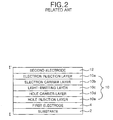
- Fig. 1 is a schematic section view showing a structure of a conventional organic EL display device
- Fig. 2 is a section view of the organic EL array taken along the I-I' line in Fig. 1.
- the organic EL array 50 has a first electrode (or anode electrode) 4 and a second electrode (or cathode electrode) 12 provided on a substrate 2 in a direction crossing each other.
- a plurality of first electrodes 4 are formed on the substrate 2 in such a manner to be spaced at a desired distance from each other.
- An insulating film 6 having an aperture for each EL cell area is formed on the substrate 2 provided with the first electrode 4.
- a barrier rib 8 for making a separation of an organic light-emitting layer 10 and the second electrode 12 to be formed thereon is positioned on the insulating film 6, and has an overhang structure in which the upper portion thereof has a larger width than the lower portion thereof.
- the organic light-emitting layer made from an organic compound and the second electrode 12 are entirely deposited onto the insulating film 6 provided with the barrier rib 8.
- the organic light-emitting layer 10 expresses red(R), green(G) and blue(B) colors. Generally, the organic light-emitting layer 10 is formed by patterning individual organic materials light-emitting red, green and blue colors for each pixel P.
- the organic light-emitting layer 10 includes a hole injection layer 10e, a hole carrier layer 10d, a light-emitting layer 10c, an electron carrier layer 10b and an electron injection layer 10a that are sequentially provided on the first electrode 4.
- the organic EL array 50 has a property liable to be deteriorated by moisture and oxygen. In order to overcome this problem, an encapsulation process is carried out. Thus, the substrate 2 provided with the organic EL array 50 is joined to a cap 28 by a sealant 26.
- Fig. 3 shows a pad portion of the conventional organic EL display device.
- a pad 37 of the pad portion of the organic EL display device shown in Fig. 3 is electrically connected to a signal supplying film 32 such as a chip on film (COF) and a tape carrier package (TCP), etc. with having an anisotropic conductive film 30 therebetween for the purpose of receiving a driving signal from the exterior thereof.
- the pad 37 has a structure in which a transparent conductive layer 36 connected to the first electrode 4 or the second electrode 12 of the organic EL array 50 and opaque conductive layer 34 are layer-built.
- indium-tin-oxide ITO
- indium-zinc-oxide IZO
- indium-tin-zinc-oxide ITZO
- Mo molybdenum
- a silicon film 38 for preventing an oxidation of the opaque conductive layer 34 caused by moisture and oxygen, etc. is provided on the opaque conductive layer 34.
- the opaque conductive film 34 provided at the pad portion of the conventional organic EL display device is corroded due to moisture (H 2 O) and oxygen (O 2 ), etc., thereby frequently causing a poor pad problem in that a driving is not applied via the signal supplying film 32.
- the opaque conductive layer 34 made from molybdenum (Mo), etc. has a property of oxidation or corrosion when it is exposed to moisture and oxygen, etc.
- Such an opaque conductive layer 34 is exposed to moisture or oxygen in the atmosphere as shown in Fig. 4 in the course of carrying out a joint process of the substrate 2 provided with the organic EL array 50 to the cap 28 and a connection process of the pad 37 to the signal supplying film 32 with having the ACF 30 therebetween, etc.
- the exposed opaque conductive layer 34 undergoes oxidation.
- oxygen and moisture are permeated into an interface among the silicon film 38, the transparent conductive layer 36 and the opaque conductive layer 34, thereby causing an oxidation of the opaque conductive layer 34.
- Such an oxidation accelerates an galvanic corrosion resulted from a difference of voltages applied to each pad 37, thereby causing a poor pad portion problem in that an external driving signal is not applied to the organic EL array 50.
- an object of the present invention to provide an organic electro-luminescence display device and a fabricating method thereof that are adaptive for preventing a badness of a pad portion.
- a pad portion of an organic electro-luminescence display device includes a first conductive layer electrically connected to any at least one of first and second electrodes of the organic electro-luminescence array; a second conductive layer provided on the first conductive layer; and a dummy insulating pattern provided to cover the first and second conductive layer and having a hole for exposing a portion of the second conductive layer.
- the organic electro-luminescence display device further includes a cap for packaging the organic electro-luminescence array; and a signal supplying film electrically connected, via said hole for exposing the second conductive layer, to the pad.
- the organic electro-luminescence display device further includes a silicon film provided at an interface area between the dummy insulating pattern and the substrate.
- the organic electro-luminescence array includes an insulating film for partially exposing the first electrode to define a light-emitting area, and said insulating film is formed from the same material as the dummy insulating pattern.
- the process of forming said pad portion includes the steps of forming a first conductive layer electrically connected to any at least one of first and second electrodes of the organic electro-luminescence array on a substrate; forming a second conductive layer on the first conductive layer; and forming a dummy insulating pattern provided to cover the first and second conductive layer and having a hole for exposing a portion of the second conductive layer.
- the method further includes the steps of joining a cap with the substrate to make a packaging of the organic electro-luminescence array; and connecting a signal supplying film, via said hole for exposing the second conductive layer, to the pad.
- the method further includes the step of forming a silicon film at an interface area between the dummy insulating pattern and the substrate.
- the organic electro-luminescence array includes an insulating film for partially exposing the first electrode to define a light-emitting area, and said insulating film is simultaneously formed from the same material as the dummy insulating pattern.
- An organic electro-luminescence display device includes an organic electro-luminescence array; and a pad for applying a driving signal to the organic electro-luminescence array and having a structure in which a first conductive layer and a second conductive layer exposing a portion of the first conductive layer are built.
- the organic electro-luminescence display device further includes a packaging plate for enclosing the organic electro-luminescence array; a signal supplying film electrically connected to the pad; and a silicon layer provided on the first conductive layer.
- the second conductive layer is partially removed from an area other than the packaging plate and the signal supplying film.
- the first conductive layer contains an oxide
- the second conductive layer contains molybdenum (Mo).
- the organic electro-luminescence array has an anode electrode and a cathode electrode, and the first conductive layer is formed from the same material as any at least one of the anode electrode and the cathode electrode.
- a method of fabricating an organic electro-luminescence display device includes the steps of forming an organic electro-luminescence array; and forming a pad having a structure in which a first conductive layer extended from the organic electro-luminescence array and a second conductive layer exposing a portion of the first conductive layer are built.
- the method further includes the steps of joining a packaging plate with the substrate in such a manner to enclose the organic electro-luminescence array; connecting a signal supplying film to the pad for the purpose of applying an external driving signal to the organic electro-luminescence array; and forming a silicon layer on the first conductive layer.
- the second conductive layer is partially removed from an area other than the packaging plate and the signal supplying film.
- the first conductive layer contains an oxide
- the second conductive layer contains molybdenum (Mo).
- the organic electro-luminescence array has an anode electrode and a cathode electrode, and the first conductive layer is formed from the same material as any at least one of the anode electrode and the cathode electrode.
- Fig. 1 is a schematic section view showing a structure of a conventional organic electro-luminescence display device
- Fig. 2 is a section view of the organic electro-luminescence array taken along the I-I' line in Fig. 1;
- Fig. 3 is a section view showing a pad portion of the conventional electro-luminescence display device
- Fig. 4 depicts a badness of the conventional pad portion
- Fig. 5 is a section view showing a portion of an organic electro-luminescence display device according to a first embodiment of the present invention
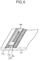
- Fig. 6 is a detailed perspective view of the pad portion A shown in Fig. 5;
- Fig. 7 is a section view of the pad portion taken along the II-II' line in Fig. 5;
- Fig. 8 is a flow chart representing a method of fabricating the organic electro-luminescence display device according to the first embodiment of the present invention.
- Fig. 9 is a section view showing a portion of an organic electro-luminescence display device according to a second embodiment of the present invention.
- Fig. 10 is a flow chart representing a method of fabricating the organic electro-luminescence display device according to the second embodiment of the present invention.
- Fig. 5 is a section view showing a portion of an organic electro-luminescence (EL) display device according to a first embodiment of the present invention
- Fig. 6 is a detailed perspective view of the pad portion A shown in Fig. 5
- Fig. 7 is a section view of the pad portion taken along the II-II' line in Fig. 5.
- EL organic electro-luminescence
- An organic EL array 150 in the organic EL display device according to the first embodiment of the present invention shown in Fig. 5 to Fig. 7 has the same structure as that in the conventional organic EL display device shown in Fig. 1 to Fig. 3.
- the organic EL array 150 has a first electrode (or anode electrode) 104 and a second electrode (or cathode electrode) 112 provided on a substrate 102 in a direction crossing each other.
- a plurality of first electrodes 104 are formed on the substrate 2 in such a manner to be spaced at a desired distance from each other.
- An insulating film 106 having an aperture for each EL cell area is formed on the substrate 102 provided with the first electrode 104.
- a barrier rib 108 for making a separation of an organic light-emitting layer 110 and the second electrode 112 to be formed thereon is positioned on the insulating film 106.
- the barrier rib 108 is provided in a direction crossing the first electrode 104, and has an overhang structure in which the upper portion thereof has a larger width than the lower portion thereof.
- the organic light-emitting layer 110 made from an organic compound and the second electrode 112 are entirely deposited onto the insulating film 106 provided with the barrier rib 108.
- a pad 137 of the pad portion of the organic EL display device is electrically connected to a signal supplying film 132 such as a chip on film (COF) and a tape carrier package (TCP), etc. with having an anisotropic conductive film (ACF) 30 therebetween for the purpose of receiving a driving signal from the exterior thereof.
- a signal supplying film 132 such as a chip on film (COF) and a tape carrier package (TCP), etc. with having an anisotropic conductive film (ACF) 30 therebetween for the purpose of receiving a driving signal from the exterior thereof.
- COF chip on film
- TCP tape carrier package
- the pad 137 includes a transparent conductive layer 136 connected to the first electrode 104 or the second electrode 112, an opaque conductive layer 134 for enhancing a conductivity of the transparent conductive layer 136, and a dummy insulating pattern 175 for covering the transparent conductive layer 136 and the opaque conductive layer 134.
- the dummy insulating pattern 175 plays a role to prevent oxidation or corrosion of the opaque conductive layer 134.
- the dummy insulating pattern 175 is provided to cover the opaque conductive layer 134 made from molybdenum (Mo) weak to moisture (H 2 O) and oxygen (O 2 ), etc., thereby allowing the opaque conductive layer 134 to be exposed to moisture (H 2 O) and oxygen (O 2 ), etc.
- Mo molybdenum
- the dummy insulating pattern 175 is provided with a contact hole 180 for exposing a portion of the opaque conductive layer 134, and the signal supplying film 132 is connected to the opaque conductive layer 134 exposed through the contact hole 180, thereby allowing it to be electrically connected to the pad 137.
- indium-tin-oxide ITO
- indium-zinc-oxide IZO
- indium-tin-zinc-oxide ITO
- molybdenum Mo
- the dummy insulating pattern 175 is formed from the same material as the insulating pattern 106 of the organic EL array 150.
- a silicon film 36 is provided on the dummy insulating pattern 175 or an interface area between the substrate 102 and the dummy insulating pattern 175, thereby reinforcing a protection of the opaque conductive layer 134.
- the pad portion of the organic EL display device includes the transparent conductive layer 136 and opaque conductive layer 134 electrically connected to any at least one of the first and second electrodes 104 and 112 of the organic EL array 150, and the dummy insulating pattern 175 provided to cover the transparent conductive layer 136 and the opaque conductive layer 134 and having the contact hole 180 for exposing a portion of the opaque conductive layer 134. Accordingly, it becomes possible to protect the opaque conductive layer 134 from moisture and oxygen, etc., thereby preventing a badness of the pad portion.
- Fig. 8 is a flow chart representing a method of fabricating the organic electro-luminescence display device according to the first embodiment of the present invention.
- the transparent conductive layer 136 connected to each of the first electrode 104 and the second electrode 112 of the organic EL array 150 is formed on the substrate 102.
- indium-tin-oxide (ITO), indium-zinc-oxide (IZO), indium-tin-zinc-oxide (ITZO) or the like is used as the transparent conductive layer 136.
- an opaque conductive material is entirely deposited onto the transparent conductive layer 136 by a deposition technique such as the sputtering, etc. and then is patterned by the photolithography and the etching process using a mask to thereby provide the opaque conductive layer 134.
- a photosensitive insulating material is deposited onto the substrate 102 provided with the first electrode, the transparent conductive layer 136 and the opaque conductive layer 134 and then is patterned by the photolithography, thereby providing the insulating film 106 of the organic EL array 150 and providing the dummy insulating pattern 175 on the opaque conductive layer 134.
- the insulating film 106 partially exposes the first electrode 104 to define a light-emitting area, whereas the dummy insulating film 175 is provided to cover the transparent conductive layer 136 and the opaque conductive layer 134 and has the contact hole 180 for exposing a portion of the opaque conductive layer 134.
- the pad 136 having a structure in which the transparent conductive 136, the opaque conductive layer 134 and the dummy insulating pattern 175 are built.
- the cap 128 is joined to the substrate 102 by the encapsulation process.
- the pad 137 is electrically connected, via the ACF 130, to the signal supplying film 132.
- the ACF 130 is connected, via the contact hole 180 of the dummy insulating pattern 175, to the opaque conductive layer 134 of the pad 137.
- the silicon film 138 is provided on the dummy insulating pattern 175 or at an interface area between the dummy insulating pattern 175 and the substrate 102.
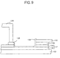
- Fig. 9 is a section view showing a portion of an organic electro-luminescence (EL) display device according to a second embodiment of the present invention.
- EL organic electro-luminescence
- the organic EL array 150 has a first electrode (or anode electrode) 104 and a second electrode (or cathode electrode) 112 provided on a substrate 102 in a direction crossing each other.
- a pad 137 of the pad area of the organic EL display device is electrically connected to a signal supplying film 132, for example, connection films such as a tape carrier package (TCP), etc. with having an anisotropic conductive film (ACF) 30 therebetween for the purpose of receiving a driving signal from the exterior thereof.
- a signal supplying film 132 for example, connection films such as a tape carrier package (TCP), etc. with having an anisotropic conductive film (ACF) 30 therebetween for the purpose of receiving a driving signal from the exterior thereof.
- the pad 137 has a structure in which a transparent conductive layer 136 connected to a first electrode 104 or a second electrode 112 of an organic EL array 150 and an opaque conductive layer 134 for enhancing a conductivity of the transparent conductive layer 136 are built.
- the opaque conductive layer 134 is provided on the transparent conductive layer 136 in such a manner to expose a portion of the transparent conductive layer 136. More specifically, the transparent conductive layer 136 is provided to expose the transparent conductive layer 136 at an area other than its area overlapping with a packaging plate 128 and a TCP 132.
- a silicon layer 134 for preventing an oxidation of the opaque conductive layer 134 caused by moisture and oxygen, etc. is provided on the opaque conductive layer 134 and the transparent conductive layer 136.
- the opaque conductive layer 134 is provided at an area overlapping with the packaging plate 128 and the TCP 132 on the transparent conductive layer 136 connected to any one of the first and second electrodes 104 and 112.
- the transparent conductive layer 136 is provided in such a manner to be exposed at an area non-overlapping with the package plate 128 and the TCP 132 of the pad area, so that it becomes possible to better prevent an oxidation of the opaque conductive layer 134 caused by moisture (H 2 O) and oxygen (O 2 ), etc. in comparison with the prior art.
- the opaque conductive layer 134 made from molybdenum (Mo) has an oxidation property when it is exposed to moisture and oxygen, etc.
- the transparent conductive layer 136 made from indium-tin-oxide (ITO), indium-zinc-oxide (IZO), indium-tin-zinc-oxide (ITZO) or the like is not oxidized due to oxygen and moisture, etc.
- the transparent conductive layer 136 contains an oxide to have a property relatively strong to an acid in comparison with the opaque conductive layer 134.
- the transparent conductive layer 136 is not oxidized even though it is exposed to moisture and oxygen in the atmosphere in the course of carrying out a joint process of the substrate 102 provided with the organic EL array 150 to the packaging plate 128 and a connection process of the pad 137 and the TCP 132 with having the ACF 130 therebetween.
- the opaque conductive layer 134 is not exposed to moisture and oxygen owing to the packaging plate 128 and the TCP 132.
- any conductive layer is not oxidized, so that a galvanic corrosion caused by a difference of voltages applied to each pad 37 also is not generated. Accordingly, it becomes possible to prevent a pad badness.
- Fig. 10 is a flow chart representing a method of fabricating the organic EL display device according to the second embodiment of the present invention.
- the organic EL array 150 is formed on the substrate 150 and, at the same time, the transparent conductive layer 136 connected to each of the first electrode 104 and the second electrode 112 of the organic EL array 150 is formed on the substrate 102.
- the transparent conductive layer 136 is used as the transparent conductive layer 136.
- an opaque conductive material is entirely deposited onto the transparent conductive layer 136 by a deposition technique such as the sputtering, etc. and then is patterned by the photolithography and the etching process using a mask to thereby provide the opaque conductive layer 134.
- the opaque conductive layer 134 is provided on an area to be overlapped with the packaging plate 128 to be joined with the substrate 102 and the TCP 132 electrically connected to the pad 137.
- the transparent conductive layer 136 at an area non-overlapping with the packaging plate 128 and the TCP 132 is exposed. Accordingly, there is provided the pad 137 having a structure in which the transparent conductive layer 136 and the opaque conductive layer 134 are built.
- the packaging plate 128 is joined to the substrate 102 by an encapsulation process.
- the pad 137 is electrically connected, via the ACF 130, to the TCP 132.
- the silicon layer 138 is formed on the exposed transparent conductive layer 136.
- the opaque conductive layer 134 is provided in such a manner to expose a portion of the transparent conductive layer 136 at an area overlapping with the packaging plate 128 and the TCP 132 on the transparent conductive layer 136 for applying a driving signal to the organic EL array.
- the opaque conductive layer 134 is not exposed to moisture (H 2 O) and oxygen (O 2 ), etc., thereby preventing an oxidation of the opaque conductive layer 134. Accordingly, it becomes possible to prevent a pad badness such as a generation of a galvanic corrosion caused by a difference of voltages applied to each pad 137.
- the pad portion includes the transparent conductive layer and the opaque conductive layer, and the dummy insulating pattern for covering the transparent conductive layer and the opaque conductive layer to protect the opaque conductive layer from moisture and oxygen, etc. Accordingly, it becomes possible to prevent a pad portion badness such as oxidation or corrosion of the opaque conductive layer.
- the opaque conductive layer is provided on the transparent conductive layer extended from the organic EL array in such a manner to expose a portion of the transparent conductive layer and overlap with the packaging plate and the TCP.
- the opaque conductive layer is not exposed to moisture (H 2 O) and oxygen (O 2 ), etc., thereby preventing an oxidation of the opaque conductive layer. Accordingly, it becomes possible to prevent a pad portion badness.
Landscapes
- Electroluminescent Light Sources (AREA)
- Devices For Indicating Variable Information By Combining Individual Elements (AREA)
Applications Claiming Priority (4)
| Application Number | Priority Date | Filing Date | Title |
|---|---|---|---|
| KR2004011583 | 2004-02-20 | ||
| KR1020040011583A KR100717327B1 (ko) | 2004-02-20 | 2004-02-20 | 유기전계발광표시장치 및 그 제조방법 |
| KR1020040074579A KR100631121B1 (ko) | 2004-09-17 | 2004-09-17 | 유기전계발광표시소자 및 그 제조방법 |
| KR2004074579 | 2004-09-17 |
Publications (2)
| Publication Number | Publication Date |
|---|---|
| EP1566838A2 true EP1566838A2 (de) | 2005-08-24 |
| EP1566838A3 EP1566838A3 (de) | 2010-09-01 |
Family
ID=34713060
Family Applications (1)
| Application Number | Title | Priority Date | Filing Date |
|---|---|---|---|
| EP20050002341 Ceased EP1566838A3 (de) | 2004-02-20 | 2005-02-04 | Organische elektrolumineszente Anzeigevorrichtung und Herstellungsverfahren |
Country Status (4)
| Country | Link |
|---|---|
| US (2) | US7358664B2 (de) |
| EP (1) | EP1566838A3 (de) |
| JP (2) | JP2005235766A (de) |
| CN (1) | CN100539245C (de) |
Cited By (2)
| Publication number | Priority date | Publication date | Assignee | Title |
|---|---|---|---|---|
| EP1921680A3 (de) * | 2006-11-10 | 2013-01-02 | Samsung Display Co., Ltd. | Organische lichtemittierende Anzeigevorrichtung und Verfahren zu ihrer Herstellung |
| EP3182476A1 (de) * | 2015-12-15 | 2017-06-21 | LG Display Co., Ltd. | Organische lichtemittierende anzeigevorrichtung |
Families Citing this family (11)
| Publication number | Priority date | Publication date | Assignee | Title |
|---|---|---|---|---|
| KR100822204B1 (ko) * | 2006-06-07 | 2008-04-17 | 삼성에스디아이 주식회사 | 유기 발광 디스플레이 장치 |
| KR100713227B1 (ko) * | 2006-06-30 | 2007-05-02 | 삼성전자주식회사 | 디스플레이장치 및 그 제조방법 |
| KR101570530B1 (ko) | 2008-10-09 | 2015-11-19 | 엘지디스플레이 주식회사 | 연성회로기판과 이를 이용한 유기전계발광표시장치 |
| KR101815255B1 (ko) * | 2010-12-16 | 2018-01-08 | 삼성디스플레이 주식회사 | 유기전계발광표시장치 및 이에 적용되는 입력패드 |
| US8755154B2 (en) | 2011-09-13 | 2014-06-17 | Seagate Technology Llc | Tuned angled uniaxial anisotropy in trilayer magnetic sensors |
| TW201405905A (zh) * | 2012-07-24 | 2014-02-01 | Ultimate Image Corp | 發光二極體平面照明單元的製法、其製品及其製品所構成的裝置 |
| CN103681765B (zh) * | 2013-12-05 | 2016-04-06 | 京东方科技集团股份有限公司 | 显示面板及其制作方法、显示装置 |
| JP6341692B2 (ja) * | 2014-02-26 | 2018-06-13 | パイオニア株式会社 | 発光装置 |
| KR102479019B1 (ko) * | 2015-03-05 | 2022-12-19 | 삼성디스플레이 주식회사 | 플렉서블 표시장치 |
| JP2018129313A (ja) * | 2018-05-15 | 2018-08-16 | パイオニア株式会社 | 発光装置 |
| JP2020038846A (ja) * | 2019-12-02 | 2020-03-12 | パイオニア株式会社 | 発光装置 |
Citations (5)
| Publication number | Priority date | Publication date | Assignee | Title |
|---|---|---|---|---|
| JP2000021566A (ja) * | 1998-06-30 | 2000-01-21 | Nippon Seiki Co Ltd | エレクトロルミネセンス |
| JP2000021567A (ja) * | 1998-07-03 | 2000-01-21 | Futaba Corp | 有機el表示素子 |
| JP2000347636A (ja) * | 1999-03-31 | 2000-12-15 | Semiconductor Energy Lab Co Ltd | 液晶表示装置 |
| US20010054868A1 (en) | 2000-06-27 | 2001-12-27 | Tohoku Pioneer Corporation | Organic electroluminescent display panel |
| JP2003272834A (ja) | 2002-03-20 | 2003-09-26 | Denso Corp | 表示装置 |
Family Cites Families (25)
| Publication number | Priority date | Publication date | Assignee | Title |
|---|---|---|---|---|
| JPH0752668B2 (ja) * | 1988-11-16 | 1995-06-05 | シャープ株式会社 | 薄膜el素子 |
| JPH11144877A (ja) * | 1997-11-10 | 1999-05-28 | Fuji Electric Co Ltd | 有機発光素子 |
| JP2000021564A (ja) | 1998-06-30 | 2000-01-21 | Nippon Seiki Co Ltd | エレクトロルミネセンス |
| EP1022931A4 (de) * | 1998-06-30 | 2004-04-07 | Nippon Seiki Co Ltd | Elektrolumineszentes bildschirm |
| TW413949B (en) * | 1998-12-12 | 2000-12-01 | Samsung Electronics Co Ltd | Thin film transistor array panels for liquid crystal displays and methods of manufacturing the same |
| JP2000357585A (ja) | 1999-06-14 | 2000-12-26 | Futaba Corp | 有機el素子 |
| JP2001102169A (ja) * | 1999-10-01 | 2001-04-13 | Sanyo Electric Co Ltd | El表示装置 |
| US6624572B1 (en) * | 2000-02-17 | 2003-09-23 | Lg Electronics, Inc. | Organic electroluminescence display panel and method for sealing the same |
| JP2001351778A (ja) * | 2000-06-08 | 2001-12-21 | Tohoku Pioneer Corp | 有機エレクトロルミネッセンス表示デバイス及びその製造方法 |
| JP2002033188A (ja) * | 2000-07-17 | 2002-01-31 | Stanley Electric Co Ltd | 有機el表示装置 |
| KR100672622B1 (ko) * | 2000-07-26 | 2007-01-23 | 엘지.필립스 엘시디 주식회사 | 액정표시장치의 패드 및 그 제조방법 |
| JP2002203673A (ja) * | 2000-12-28 | 2002-07-19 | Katsufumi Takahashi | El電極の導線接続方法 |
| KR100682377B1 (ko) * | 2001-05-25 | 2007-02-15 | 삼성전자주식회사 | 유기 전계발광 디바이스 및 이의 제조 방법 |
| JP4244120B2 (ja) * | 2001-06-20 | 2009-03-25 | 株式会社半導体エネルギー研究所 | 発光装置及びその作製方法 |
| KR100768182B1 (ko) * | 2001-10-26 | 2007-10-17 | 삼성에스디아이 주식회사 | 유기 전자 발광 소자와 그 제조방법 |
| US6815723B2 (en) * | 2001-12-28 | 2004-11-09 | Semiconductor Energy Laboratory Co., Ltd. | Light emitting device, method of manufacturing the same, and manufacturing apparatus therefor |
| JP2003217835A (ja) | 2002-01-17 | 2003-07-31 | Nippon Seiki Co Ltd | 電界発光素子 |
| US7098069B2 (en) * | 2002-01-24 | 2006-08-29 | Semiconductor Energy Laboratory Co., Ltd. | Light emitting device, method of preparing the same and device for fabricating the same |
| JP4271915B2 (ja) * | 2002-04-11 | 2009-06-03 | オプトレックス株式会社 | 有機エレクトロルミネセンス表示素子、有機エレクトロルミネセンス表示装置 |
| FR2841724A1 (fr) * | 2002-06-28 | 2004-01-02 | Thomson Licensing Sa | Systeme et procede de synchronisation pour programmes audiovisuels, dispositifs et procedes associes |
| JP2004119304A (ja) * | 2002-09-27 | 2004-04-15 | Sanyo Electric Co Ltd | 有機エレクトロルミネッセンス表示装置およびその製造方法 |
| US6936407B2 (en) * | 2003-02-28 | 2005-08-30 | Osram Opto Semiconductors Gmbh | Thin-film electronic device module |
| US7026660B2 (en) * | 2003-04-25 | 2006-04-11 | Osram Opto Semiconductors (Malaysia) Sdn. Bhd | Interconnection for organic devices |
| KR100692850B1 (ko) * | 2003-07-31 | 2007-03-13 | 엘지전자 주식회사 | 전계 발광 표시장치 및 그 제조방법 |
| JP2005183209A (ja) * | 2003-12-19 | 2005-07-07 | Asahi Glass Co Ltd | 有機el表示装置及びその製造方法 |
-
2005
- 2005-02-04 EP EP20050002341 patent/EP1566838A3/de not_active Ceased
- 2005-02-16 US US11/058,607 patent/US7358664B2/en not_active Expired - Lifetime
- 2005-02-16 JP JP2005039392A patent/JP2005235766A/ja active Pending
- 2005-02-17 CN CNB2005100083630A patent/CN100539245C/zh not_active Expired - Fee Related
-
2007
- 2007-07-18 US US11/826,762 patent/US7919919B2/en not_active Expired - Fee Related
-
2010
- 2010-12-28 JP JP2010292313A patent/JP2011066017A/ja active Pending
Patent Citations (5)
| Publication number | Priority date | Publication date | Assignee | Title |
|---|---|---|---|---|
| JP2000021566A (ja) * | 1998-06-30 | 2000-01-21 | Nippon Seiki Co Ltd | エレクトロルミネセンス |
| JP2000021567A (ja) * | 1998-07-03 | 2000-01-21 | Futaba Corp | 有機el表示素子 |
| JP2000347636A (ja) * | 1999-03-31 | 2000-12-15 | Semiconductor Energy Lab Co Ltd | 液晶表示装置 |
| US20010054868A1 (en) | 2000-06-27 | 2001-12-27 | Tohoku Pioneer Corporation | Organic electroluminescent display panel |
| JP2003272834A (ja) | 2002-03-20 | 2003-09-26 | Denso Corp | 表示装置 |
Cited By (2)
| Publication number | Priority date | Publication date | Assignee | Title |
|---|---|---|---|---|
| EP1921680A3 (de) * | 2006-11-10 | 2013-01-02 | Samsung Display Co., Ltd. | Organische lichtemittierende Anzeigevorrichtung und Verfahren zu ihrer Herstellung |
| EP3182476A1 (de) * | 2015-12-15 | 2017-06-21 | LG Display Co., Ltd. | Organische lichtemittierende anzeigevorrichtung |
Also Published As
| Publication number | Publication date |
|---|---|
| US7919919B2 (en) | 2011-04-05 |
| US20070262711A1 (en) | 2007-11-15 |
| JP2005235766A (ja) | 2005-09-02 |
| EP1566838A3 (de) | 2010-09-01 |
| JP2011066017A (ja) | 2011-03-31 |
| US7358664B2 (en) | 2008-04-15 |
| CN100539245C (zh) | 2009-09-09 |
| CN1658715A (zh) | 2005-08-24 |
| US20050184656A1 (en) | 2005-08-25 |
Similar Documents
| Publication | Publication Date | Title |
|---|---|---|
| US7919919B2 (en) | Organic electroluminescent display having a specific structure for a pad supplying the drive signal | |
| US7851994B2 (en) | Organic electro-luminescence display device with an organic electro-luminescence array and fabricating method thereof | |
| CN100505289C (zh) | 有机电致发光显示器件及其制造方法 | |
| JPH11144865A (ja) | 有機エレクトロルミネッセンス素子の製造方法 | |
| KR100755398B1 (ko) | 유기전계발광표시소자 및 그 제조방법 | |
| US20100136723A1 (en) | Dual panel-type organic electroluminescent display device | |
| JP5057007B2 (ja) | 有機電界発光表示装置及びその製造方法 | |
| KR100717327B1 (ko) | 유기전계발광표시장치 및 그 제조방법 | |
| KR20020043324A (ko) | 유기 전계 발광 표시장치 및 그 제조 방법 | |
| KR100631121B1 (ko) | 유기전계발광표시소자 및 그 제조방법 | |
| KR20050097569A (ko) | 유기 전계발광 표시소자 및 그 제조방법 | |
| US7486018B2 (en) | Organic electro-luminescence display device and fabricating method thereof | |
| CN1694594B (zh) | 有机电致发光显示设备及其制造方法 | |
| KR100571003B1 (ko) | 평판 표시 장치 및 그 제조 방법 | |
| KR100623450B1 (ko) | 유기 전계발광 표시소자 및 그 제조방법 | |
| KR100726942B1 (ko) | 유기 전계발광 표시장치 및 그 제조방법 | |
| KR100692873B1 (ko) | 마스크 장치 및 이를 이용한 유기전계발광표시소자의제조방법 | |
| KR20090019207A (ko) | 티자형 격벽과 이를 포함하는 유기전계발광 소자 및 그의제조방법 | |
| KR100726943B1 (ko) | 유기 전계발광 표시장치 및 그 제조방법 | |
| KR100726954B1 (ko) | 유기전계발광표시장치 및 그 제조방법 | |
| KR20100064586A (ko) | 표시소자 및 그의 제조방법 | |
| KR20070038755A (ko) | 유기 전계발광 표시장치 및 그 제조방법 |
Legal Events
| Date | Code | Title | Description |
|---|---|---|---|
| PUAI | Public reference made under article 153(3) epc to a published international application that has entered the european phase |
Free format text: ORIGINAL CODE: 0009012 |
|
| 17P | Request for examination filed |
Effective date: 20050204 |
|
| AK | Designated contracting states |
Kind code of ref document: A2 Designated state(s): AT BE BG CH CY CZ DE DK EE ES FI FR GB GR HU IE IS IT LI LT LU MC NL PL PT RO SE SI SK TR |
|
| AX | Request for extension of the european patent |
Extension state: AL BA HR LV MK YU |
|
| PUAL | Search report despatched |
Free format text: ORIGINAL CODE: 0009013 |
|
| AK | Designated contracting states |
Kind code of ref document: A3 Designated state(s): AT BE BG CH CY CZ DE DK EE ES FI FR GB GR HU IE IS IT LI LT LU MC NL PL PT RO SE SI SK TR |
|
| AX | Request for extension of the european patent |
Extension state: AL BA HR LV MK YU |
|
| AKX | Designation fees paid |
Designated state(s): AT BE BG CH CY CZ DE DK EE ES FI FR GB GR HU IE IS IT LI LT LU MC NL PL PT RO SE SI SK TR |
|
| 17Q | First examination report despatched |
Effective date: 20110915 |
|
| STAA | Information on the status of an ep patent application or granted ep patent |
Free format text: STATUS: THE APPLICATION HAS BEEN REFUSED |
|
| 18R | Application refused |
Effective date: 20150506 |