EP1564796A1 - Procédé de production des plaquettes semi-conductrices et plaquettes ainsi obtenues - Google Patents
Procédé de production des plaquettes semi-conductrices et plaquettes ainsi obtenues Download PDFInfo
- Publication number
- EP1564796A1 EP1564796A1 EP05010508A EP05010508A EP1564796A1 EP 1564796 A1 EP1564796 A1 EP 1564796A1 EP 05010508 A EP05010508 A EP 05010508A EP 05010508 A EP05010508 A EP 05010508A EP 1564796 A1 EP1564796 A1 EP 1564796A1
- Authority
- EP
- European Patent Office
- Prior art keywords
- etching
- acid
- controlled
- reaction
- acid etching
- Prior art date
- Legal status (The legal status is an assumption and is not a legal conclusion. Google has not performed a legal analysis and makes no representation as to the accuracy of the status listed.)
- Withdrawn
Links
- 239000004065 semiconductor Substances 0.000 title claims abstract description 26
- 235000012431 wafers Nutrition 0.000 title description 124
- 238000003672 processing method Methods 0.000 title description 7
- 238000005530 etching Methods 0.000 claims abstract description 412
- 239000002253 acid Substances 0.000 claims abstract description 220
- 238000006243 chemical reaction Methods 0.000 claims abstract description 85
- 238000009792 diffusion process Methods 0.000 claims abstract description 55
- 238000000034 method Methods 0.000 claims abstract description 22
- 238000005498 polishing Methods 0.000 claims abstract description 22
- 238000012545 processing Methods 0.000 claims abstract description 10
- 238000004140 cleaning Methods 0.000 claims abstract description 5
- QTBSBXVTEAMEQO-UHFFFAOYSA-N Acetic acid Chemical compound CC(O)=O QTBSBXVTEAMEQO-UHFFFAOYSA-N 0.000 claims description 51
- XUIMIQQOPSSXEZ-UHFFFAOYSA-N Silicon Chemical compound [Si] XUIMIQQOPSSXEZ-UHFFFAOYSA-N 0.000 claims description 37
- 229910052710 silicon Inorganic materials 0.000 claims description 37
- 239000010703 silicon Substances 0.000 claims description 37
- KRHYYFGTRYWZRS-UHFFFAOYSA-N Fluorane Chemical compound F KRHYYFGTRYWZRS-UHFFFAOYSA-N 0.000 claims description 34
- 239000007864 aqueous solution Substances 0.000 claims description 30
- GRYLNZFGIOXLOG-UHFFFAOYSA-N Nitric acid Chemical compound O[N+]([O-])=O GRYLNZFGIOXLOG-UHFFFAOYSA-N 0.000 claims description 17
- 229910017604 nitric acid Inorganic materials 0.000 claims description 17
- XLYOFNOQVPJJNP-UHFFFAOYSA-N water Substances O XLYOFNOQVPJJNP-UHFFFAOYSA-N 0.000 claims description 10
- 230000003746 surface roughness Effects 0.000 abstract description 35
- 230000007423 decrease Effects 0.000 abstract description 29
- 239000002245 particle Substances 0.000 abstract description 13
- 238000011109 contamination Methods 0.000 abstract description 7
- 239000003513 alkali Substances 0.000 description 62
- 230000003247 decreasing effect Effects 0.000 description 20
- MHAJPDPJQMAIIY-UHFFFAOYSA-N Hydrogen peroxide Chemical compound OO MHAJPDPJQMAIIY-UHFFFAOYSA-N 0.000 description 16
- 230000000694 effects Effects 0.000 description 14
- HEMHJVSKTPXQMS-UHFFFAOYSA-M Sodium hydroxide Chemical compound [OH-].[Na+] HEMHJVSKTPXQMS-UHFFFAOYSA-M 0.000 description 12
- 230000000052 comparative effect Effects 0.000 description 12
- 239000006061 abrasive grain Substances 0.000 description 10
- 238000004090 dissolution Methods 0.000 description 7
- 239000000243 solution Substances 0.000 description 7
- 238000005259 measurement Methods 0.000 description 5
- 239000000203 mixture Substances 0.000 description 4
- 150000001875 compounds Chemical class 0.000 description 3
- NBIIXXVUZAFLBC-UHFFFAOYSA-N Phosphoric acid Chemical compound OP(O)(O)=O NBIIXXVUZAFLBC-UHFFFAOYSA-N 0.000 description 2
- QAOWNCQODCNURD-UHFFFAOYSA-N Sulfuric acid Chemical compound OS(O)(=O)=O QAOWNCQODCNURD-UHFFFAOYSA-N 0.000 description 2
- 238000013459 approach Methods 0.000 description 2
- 238000003486 chemical etching Methods 0.000 description 2
- 230000002209 hydrophobic effect Effects 0.000 description 2
- 238000007654 immersion Methods 0.000 description 2
- 238000011835 investigation Methods 0.000 description 2
- 230000003287 optical effect Effects 0.000 description 2
- LPXPTNMVRIOKMN-UHFFFAOYSA-M sodium nitrite Chemical compound [Na+].[O-]N=O LPXPTNMVRIOKMN-UHFFFAOYSA-M 0.000 description 2
- 239000000126 substance Substances 0.000 description 2
- 229910001218 Gallium arsenide Inorganic materials 0.000 description 1
- IOVCWXUNBOPUCH-UHFFFAOYSA-M Nitrite anion Chemical compound [O-]N=O IOVCWXUNBOPUCH-UHFFFAOYSA-M 0.000 description 1
- 239000000654 additive Substances 0.000 description 1
- 229910000147 aluminium phosphate Inorganic materials 0.000 description 1
- 230000015556 catabolic process Effects 0.000 description 1
- 238000006731 degradation reaction Methods 0.000 description 1
- 238000010586 diagram Methods 0.000 description 1
- 238000006073 displacement reaction Methods 0.000 description 1
- 239000007789 gas Substances 0.000 description 1
- 238000010438 heat treatment Methods 0.000 description 1
- 238000003754 machining Methods 0.000 description 1
- 238000004519 manufacturing process Methods 0.000 description 1
- 239000000463 material Substances 0.000 description 1
- 229910021421 monocrystalline silicon Inorganic materials 0.000 description 1
- 239000002736 nonionic surfactant Substances 0.000 description 1
- 230000036632 reaction speed Effects 0.000 description 1
- 230000001629 suppression Effects 0.000 description 1
- 239000004094 surface-active agent Substances 0.000 description 1
- 238000011179 visual inspection Methods 0.000 description 1
Images


Classifications
-
- H—ELECTRICITY
- H01—ELECTRIC ELEMENTS
- H01L—SEMICONDUCTOR DEVICES NOT COVERED BY CLASS H10
- H01L21/00—Processes or apparatus adapted for the manufacture or treatment of semiconductor or solid state devices or of parts thereof
- H01L21/02—Manufacture or treatment of semiconductor devices or of parts thereof
- H01L21/02041—Cleaning
- H01L21/02043—Cleaning before device manufacture, i.e. Begin-Of-Line process
- H01L21/02052—Wet cleaning only
-
- H—ELECTRICITY
- H01—ELECTRIC ELEMENTS
- H01L—SEMICONDUCTOR DEVICES NOT COVERED BY CLASS H10
- H01L21/00—Processes or apparatus adapted for the manufacture or treatment of semiconductor or solid state devices or of parts thereof
- H01L21/02—Manufacture or treatment of semiconductor devices or of parts thereof
- H01L21/02002—Preparing wafers
- H01L21/02005—Preparing bulk and homogeneous wafers
- H01L21/02008—Multistep processes
- H01L21/0201—Specific process step
- H01L21/02019—Chemical etching
-
- H—ELECTRICITY
- H01—ELECTRIC ELEMENTS
- H01L—SEMICONDUCTOR DEVICES NOT COVERED BY CLASS H10
- H01L21/00—Processes or apparatus adapted for the manufacture or treatment of semiconductor or solid state devices or of parts thereof
- H01L21/02—Manufacture or treatment of semiconductor devices or of parts thereof
- H01L21/04—Manufacture or treatment of semiconductor devices or of parts thereof the devices having potential barriers, e.g. a PN junction, depletion layer or carrier concentration layer
- H01L21/18—Manufacture or treatment of semiconductor devices or of parts thereof the devices having potential barriers, e.g. a PN junction, depletion layer or carrier concentration layer the devices having semiconductor bodies comprising elements of Group IV of the Periodic Table or AIIIBV compounds with or without impurities, e.g. doping materials
- H01L21/30—Treatment of semiconductor bodies using processes or apparatus not provided for in groups H01L21/20 - H01L21/26
- H01L21/302—Treatment of semiconductor bodies using processes or apparatus not provided for in groups H01L21/20 - H01L21/26 to change their surface-physical characteristics or shape, e.g. etching, polishing, cutting
- H01L21/306—Chemical or electrical treatment, e.g. electrolytic etching
- H01L21/30604—Chemical etching
- H01L21/30608—Anisotropic liquid etching
-
- Y—GENERAL TAGGING OF NEW TECHNOLOGICAL DEVELOPMENTS; GENERAL TAGGING OF CROSS-SECTIONAL TECHNOLOGIES SPANNING OVER SEVERAL SECTIONS OF THE IPC; TECHNICAL SUBJECTS COVERED BY FORMER USPC CROSS-REFERENCE ART COLLECTIONS [XRACs] AND DIGESTS
- Y10—TECHNICAL SUBJECTS COVERED BY FORMER USPC
- Y10S—TECHNICAL SUBJECTS COVERED BY FORMER USPC CROSS-REFERENCE ART COLLECTIONS [XRACs] AND DIGESTS
- Y10S438/00—Semiconductor device manufacturing: process
- Y10S438/928—Front and rear surface processing
-
- Y—GENERAL TAGGING OF NEW TECHNOLOGICAL DEVELOPMENTS; GENERAL TAGGING OF CROSS-SECTIONAL TECHNOLOGIES SPANNING OVER SEVERAL SECTIONS OF THE IPC; TECHNICAL SUBJECTS COVERED BY FORMER USPC CROSS-REFERENCE ART COLLECTIONS [XRACs] AND DIGESTS
- Y10—TECHNICAL SUBJECTS COVERED BY FORMER USPC
- Y10S—TECHNICAL SUBJECTS COVERED BY FORMER USPC CROSS-REFERENCE ART COLLECTIONS [XRACs] AND DIGESTS
- Y10S438/00—Semiconductor device manufacturing: process
- Y10S438/959—Mechanical polishing of wafer
-
- Y—GENERAL TAGGING OF NEW TECHNOLOGICAL DEVELOPMENTS; GENERAL TAGGING OF CROSS-SECTIONAL TECHNOLOGIES SPANNING OVER SEVERAL SECTIONS OF THE IPC; TECHNICAL SUBJECTS COVERED BY FORMER USPC CROSS-REFERENCE ART COLLECTIONS [XRACs] AND DIGESTS
- Y10—TECHNICAL SUBJECTS COVERED BY FORMER USPC
- Y10S—TECHNICAL SUBJECTS COVERED BY FORMER USPC CROSS-REFERENCE ART COLLECTIONS [XRACs] AND DIGESTS
- Y10S438/00—Semiconductor device manufacturing: process
- Y10S438/974—Substrate surface preparation
-
- Y—GENERAL TAGGING OF NEW TECHNOLOGICAL DEVELOPMENTS; GENERAL TAGGING OF CROSS-SECTIONAL TECHNOLOGIES SPANNING OVER SEVERAL SECTIONS OF THE IPC; TECHNICAL SUBJECTS COVERED BY FORMER USPC CROSS-REFERENCE ART COLLECTIONS [XRACs] AND DIGESTS
- Y10—TECHNICAL SUBJECTS COVERED BY FORMER USPC
- Y10S—TECHNICAL SUBJECTS COVERED BY FORMER USPC CROSS-REFERENCE ART COLLECTIONS [XRACs] AND DIGESTS
- Y10S438/00—Semiconductor device manufacturing: process
- Y10S438/977—Thinning or removal of substrate
Definitions
- the present invention relates to an improvement on the method of removing, through chemical etching, a damaged layer that is generated on the surface of a monocrystalline silicon wafer during a process of producing the wafer.
- a conventional process of producing a mirror-polished semiconductor wafer typically comprises the steps of slicing a monocrystalline ingot of silicon or the like to obtain a semiconductor wafer; and chamfering, lapping, acid etching, mirror-polishing, and cleaning the sliced semiconductor wafer.
- the sequence of steps is changed; some steps are repeated a plurality of times; or other steps such as heat treatment and grinding are added to or replace the above-described steps.
- steps are performed in accordance with the specifications.
- acid etching is performed for the purpose of removing a surface damaged layer introduced in the course of mechanical machining steps such as slicing, chamfering, and lapping.
- the surface of a wafer is etched to a depth of a few to a few tens of microns through use of mixed acid aqueous solution composed of hydrofluoric acid, nitric acid, acetic acid, and water.
- acid etching involves the following problems:
- particles generated in a subsequent step and a polishing stock removal in a mirror-polishing step can be decreased if etching treatment can be performed while flatness attained through lapping is maintained, so as to remove a mechanically formed damage layer, improve the surface roughness, efficiently decrease the depth of deep pits locally formed due to the etching, and smooth the uneven shape of the surface.
- the present invention has been accomplished to solve the above-mentioned problems, and an object of the invention is to provide a method of processing a semiconductor wafer which can remove a mechanically formed damage layer, improve surface roughness, and efficiently decrease the depth of locally formed deep pits, while the flatness of the wafer attained through lapping is maintained, in order to produce a chemically etched wafer (CW) having a smooth and flat etched surface that hardly causes generation of particles and contamination.
- CW chemically etched wafer
- Another object of the invention is to provide a semiconductor wafer processed through the above-described processing method.
- the present invention provides a method of processing a semiconductor wafer sliced from a monocrystalline ingot.
- the method comprises at least the steps of chamfering, lapping, etching, mirror-polishing, and cleaning and is characterized in that in the etching step alkali etching is first performed and then acid etching is performed, and that an etching amount of the alkali etching is greater than an etching amount of the acid etching.
- etching step of the processing method of the present invention after the step of lapping alkali etching is first performed in order to remove a mechanically formed damage layer, while the flatness of the wafer attained through lapping is maintained, and subsequently, acid etching is performed in order to decrease the depth of locally formed deep pits remaining after the alkali etching and to improve the surface roughness and the sharp uneven shape.
- the etching amount of the alkali etching must be set greater than the etching amount of the acid etching because of the following reasons. That is, in order to decrease the depth of locally formed deep pits remaining after the alkali etching, the etching amount of the alkali etching must be increased to a certain level, which is greater than the etching amount of the acid etching required for decreasing the rate of generation of faults such as stain stemming from unevenness in etching and for improving flatness.
- a wafer that has undergone the alkali etching is immersed into aqueous solution of hydrogen peroxide.
- the surface of a wafer that has undergone the alkali etching is active and hydrophobic, so that foreign matter easily adheres and dirties the wafer.
- the surface of the wafer is oxidized through immersion into aqueous solution of hydrogen peroxide and thus made hydrophilic, particles hardly adhere to the wafer surface.
- the etching amount of the alkali etching is 10 - 30 ⁇ m, and the etching amount of the acid etching is 5 - 20 ⁇ m.
- the etching amount of the alkali etching is maintained within the above-described range.
- the stain generation rate decreases considerably although the flatness deteriorates. Therefore, the etching amount of the acid etching is maintained within the above-described range.
- the etchant used in the alkali etching is an aqueous solution of NaOH or KOH
- the etchant used in the acid etching is a mixed acid aqueous solution composed of hydrofluoric acid, nitric acid, acetic acid, and water.
- etching is performed effectively and reliably in both the alkali etching and the acid etching, and the respective etching amounts can be controlled with relative ease.
- the etching can be performed at low cost.
- each specific value used in relation to etching amount represents the sum of the thicknesses of layers removed, through etching, from opposites surfaces of a wafer.
- the acid etching is reaction-controlled acid etching.
- the flatness can be further improved through suppression of waviness, while realizing a decrease in the depth of deep pits locally remaining after the alkali etching and improvement of the surface roughness and the sharp uneven shape.
- an etchant obtained through addition of 20 - 30 g/l of silicon into a mixed acid aqueous solution composed of hydrofluoric acid, nitric acid, acetic acid, and water.
- etching is performed effectively and reliably, and the etching amount can be controlled with relative ease.
- the etching can be performed at low cost.
- the present invention provides another method of processing a semiconductor wafer sliced from a monocrystalline ingot.
- the method comprises at least the steps of chamfering, lapping, etching, mirror-polishing, and cleaning and is characterized in that in the etching step reaction-controlled acid etching is first performed and then diffusion-controlled acid etching is performed, and that an etching amount of the reaction-controlled acid etching is greater than an etching amount of the diffusion-controlled acid etching.
- reaction-controlled acid etching is first performed for a lapped wafer in order to remove a mechanically formed damage layer, while the flatness of the wafer attained through lapping is maintained, and subsequently, diffusion-controlled acid etching is performed in order to decrease the depth of deep pits remaining after the reaction-controlled acid etching and to improve the surface roughness and the sharp uneven shape.
- the etching amount of the reaction-controlled acid etching must be set greater than the etching amount of the diffusion-controlled acid etching because of the following reasons. That is, in order to decrease the depth of locally formed deep pits remaining after the reaction-controlled acid etching, the etching amount of the reaction-controlled acid etching must be increased to a certain level, which is greater than the etching amount of the diffusion-controlled acid etching required for decreasing the rate of generation of faults such as stain stemming from unevenness in etching and for improving flatness.
- the etching amount of the reaction-controlled acid etching is 10 - 30 ⁇ m, and the etching amount of the diffusion-controlled acid etching is 5 - 20 ⁇ m.
- the etching amount of the reaction-controlled acid etching is maintained within the above-described range.
- the stain generation rate decreases considerably although flatness deteriorates. Therefore, the etching amount of the diffusion-controlled acid etching is maintained within the above-described range.
- each of the reaction-controlled acid etching and the diffusion-controlled acid etching there is used an etchant obtained through addition of silicon to a mixed acid aqueous solution composed of hydrofluoric acid, nitric acid, acetic acid, and water, and the silicon concentration of the etchant used in the reaction-controlled acid etching is higher than that of the etchant used in the diffusion-controlled acid etching.
- etching is performed effectively and reliably in both the reaction-controlled acid etching and the diffusion-controlled acid etching, and the respective etching amounts can be controlled with relative ease.
- the etching can be performed at low cost.
- the silicon concentration of the etchant used in the reaction-controlled acid etching is 20 - 30 g/l, and the silicon concentration of the etchant used in the diffusion-controlled acid etching is 5 - 15 g/l.
- the silicon concentration of the etchant used in the reaction-controlled acid etching is less than 20 g/l, the etchant becomes a diffusion-controlled-type acid, so that flatness deteriorates.
- the silicon concentration of the etchant used in the reaction-controlled acid etching exceeds 30 g/l, the etching rate decreases, and a longer period of time is required for dissolving silicon in a mixed acid aqueous solution in order to prepare the etchant. Therefore, the silicon concentration of the etchant used in the reaction-controlled acid etching is preferably adjusted to fall within the range of 20 to 30 g/l.
- reaction-controlled type acid etchants are used, etching is performed effectively and reliably, and the etching amount can be controlled with relative ease. In addition, the etching can be performed at low cost.
- the silicon concentration of the etchant used in the diffusion-controlled acid etching is preferably adjusted to fall within the range of 5 to 15 g/l.
- the present invention further provides a semiconductor wafer processed by either one of the above-described methods of the present invention.
- alkali etching is first performed in order to remove a mechanically formed damage layer, while the flatness of the wafer attained through lapping is maintained, and subsequently, acid etching is performed. Therefore, there can be obtained a semiconductor wafer in which the depth of deep pits remaining after the alkali etching is decreased and the surface roughness and the sharp uneven shape are improved.
- reaction-controlled acid etching is employed as the acid etching, the degree of waviness decreases, so that a semiconductor wafer having a flatter surface can be produced.
- the above-described wafer can be obtained through the other method of the present invention, in which reaction-controlled acid etching is first performed and then diffusion-controlled acid etching is performed and in which the etching amount of the reaction-controlled acid etching is greater than the etching amount of the diffusion-controlled acid etching.
- the present invention further provides a semiconductor wafer in which an LTV max measured in cells of 20x20 mm is 0.3 ⁇ m or less, and the maximal value of pit depth is 6 ⁇ m or less.
- the average value of waviness of the semiconductor wafer is preferably 0.04 ⁇ m or less.
- the flatness of the wafer attained through lapping is maintained; the degree of waviness of the wafer surface after etching is decreased; deep pits are prevented from being locally generated; and degradation of surface roughness is suppressed.
- a chemically etched wafer having a smooth and flat etched surface that hardly causes generation of particles and contamination such as stain. Therefore, the amount of stock removal in a mirror-polishing step can be decreased, and the flatness of the wafer can be improved.
- the inventors of the present invention performed various studies on a method of processing a semiconductor wafer, especially on the etching method, that can produce a chemically etched wafer which maintains its flatness attained through lapping and which has an etched surface that hardly causes generation of particles and contamination.
- the inventors of the present invention conceived a wafer processing method in which alkali etching is first performed in order to remove a damage layer, while the flatness of the wafer attained through lapping is maintained, and subsequently, acid etching is performed in order to decrease the depth of remaining deep pits and to improve the surface roughness while decreasing the degree of waviness, as well as a wafer processing method in which reaction-controlled acid etching is performed as the above-described acid etching.
- the present invention was achieved on the basis of this concept and through thorough investigations of other conditions.
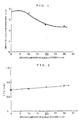
- FIG. 1 shows the relationship between etching amount and depth of locally formed deep pits in 8-inch wafers which were alkali-etched at 85°C through use of an aqueous 50% NaOH solution after being lapped by use of #1200 lapping abrasive grains.
- FIG. 2 shows the relationship between etching amount and TTV (flatness) in the 8-inch wafers
- FIG. 3 shows the relationship between etching amount and surface roughness (Ra) in the 8-inch wafers.
- the locally formed deep pits are formed as follows. When lapping abrasive grains stick in the surface of a wafer during lapping, there are formed pits, whose diameter and depth are then increased due to alkali etching. Thus, deep pits are formed. When the concentration of the alkaline compound is low, the pit depth tends to increase. When the concentration of an alkaline compound is high, the pit depth can be decreased. However, in this case, the etching amount must be increased, resulting in a lowered efficiency. The pit depth is determined based on the focal depth of an optical microscope.
- Such pits must be removed through polishing in a subsequent mirror-polishing step, and therefore the polishing stock removal in the mirror-polishing step must be set greater than the maximum value of the depth of such deep pits. Accordingly, the depth of pits is desirably decreased to a possible extent.
- TTV Total Thickness Variation
- ⁇ m represents the difference between the thickness of a thickest portion and that of a thinnest portion of a single wafer and is an indication of wafer flatness.
- LTV Local Thickness Variation
- ⁇ m represents the difference between the thickness of a thickest portion and that of a thinnest portion within each of cells (typically 20 x 20 mm, or 25 x 25 mm) defined on a single wafer.
- the LTV of each cell is called LTV cbc
- LTV max the maximum LTV within a single wafer.
- Ra ( ⁇ m) represents an arithmetical mean deviation of profile, which is the most commonly used parameter of surface roughness.
- the etching amount of alkali etching in order to decrease the depth of locally formed deep pits, the etching amount of alkali etching must be set to not less than 10 ⁇ m. As is understood from FIG. 2, in order to decrease TTV to 1 ⁇ m or less, the etching amount of alkali etching must be set to 30 ⁇ m or less. As is understood from FIG. 3, in order to decrease Ra to 0.25 ⁇ m or less, the etching amount of alkali etching must be set to 30 ⁇ m or less. In consideration of the above, a suitable range of the etching amount of the alkali etching is 10 to 30 ⁇ m. Especially, an etching amount of about 20 ⁇ m is preferred because the depth of locally formed deep pits approaches its minimal value (approximately 5 ⁇ m), and TTV and Ra do not increase greatly.
- silicon is dissolved in the mixed acid etchant with a concentration of 10 g/l to improve controlability of etching rate. Consequently this acid etching is diffusion-controlled type.
- FIG. 5 shows the relationship between etching amount and stain generation rate due to uneven etching in wafers that were chemically etched through acid etching. The generation of stain was determined through visual inspection under collimated light.
- the etching amount of acid etching in order to avoid generation of stain, the etching amount of acid etching must be set to not less than 5 ⁇ m, and in order to reliably eliminate stain, the etching amount of acid etching must be set to not less than 10 ⁇ m. As is understood from FIG. 4, in order to decrease TTV to 1 ⁇ m or less, the etching amount of acid etching must be set to 20 ⁇ m or less. In consideration of the above, a suitable range of the etching amount of the acid etching is 5 to 20 ⁇ m, and the etching amount is preferably set to approximately 10 ⁇ m.
- alkali etching and acid etching are both used, and the acid etching is performed after the alkali etching in order to fully utilize the characteristics of both etchings, so that a sufficient degree of etching effect is attained.
- alkali etching is first performed in order to remove a mechanically formed damage layer, while the flatness of the wafer attained through lapping is maintained, and acid etching is then performed.
- the depth of locally formed deep pits remaining after the alkali etching can be decreased; the surface uneven shape can be smoothed in order to improve the surface roughness; and the stain generation rate can be decreased.
- the etching amount of the alkali etching must be set greater than the etching amount of the acid etching because of the following reasons. That is, in order to decrease the depth of locally formed deep pits remaining after the alkali etching, the etching amount of the alkali etching must be increased to a certain level, which is greater than the etching amount of the acid etching required for decreasing the rate of generation of stain and for improving flatness.
- a wafer that has undergone the alkali etching is preferably immersed into aqueous solution of hydrogen peroxide before being subjected to the acid etching.
- the surface of a wafer that has undergone the alkali etching is active and hydrophobic, so that foreign matter easily adheres and dirties the wafer.
- the surface of the wafer is oxidized and thus made hydrophilic, so that particles hardly adhere to the wafer surface, which particles would otherwise contaminate an acid etchant used in the subsequent step.
- the concentration of hydrogen peroxide is preferably set to 0.1 - 30%. Concentrations less than 0.1% cannot make the surface of a wafer hydrophilic to a sufficient degree. A concentration as high as 30% provides a sufficient effect, and therefore concentrations higher than 30% are disadvantageous from a viewpoint of economy.
- reaction-controlled acid etching there is used an etchant obtained through dissolution of 20 - 30 g/l of silicon into a mixed acid aqueous solution composed of hydrofluoric acid, nitric acid, acetic acid, and water.
- the mixed acid aqueous solution causes an etching action relatively close to that of alkali etchant.
- the etchant used in the reaction-controlled acid etching is called a reaction-controlled acid etchant because its reaction speed is controlled or determined, in contrast to an ordinarily mixed acid aqueous solution used in ordinary acid etching, which is a diffusion-controlled acid.
- reaction-controlled acid etching is combined with the alkali etching
- alkali etching is first performed in order to' remove a mechanically formed damage layer, while the flatness of the wafer attained through lapping is maintained, and the reaction-controlled acid etching is then performed.
- the depth of locally formed deep pits remaining after the alkali etching can be decreased; the surface uneven shape can be smoothed in order to improve the surface roughness; and the stain generation rate can be decreased.
- the degree of waviness can be decreased compared to the case where diffusion-controlled acid etching is performed, the flatness of the wafer can be further improved.
- the above-described two-stage chemical etching i.e., alkali etching plus acid etching, according to the present invention enables easy and stable production of a semiconductor wafer which has a flatness (LTV max in 20 x 20 mm cells) of 0.3 ⁇ m or less and a maximum pit depth of 6 ⁇ m or less.
- a semiconductor wafer can be processed to have an excellent flatness in a large area such that the average value of waviness is 0.04 ⁇ m or less.
- the inventors of the present invention performed various studies on a method of processing a semiconductor wafer that can produce a chemically etched wafer which maintains its flatness attained through lapping and which has an etched surface that hardly causes generation of particles and contamination, especially studies on the etching method. Based on the studies, the inventors of the present invention conceived a wafer processing method in which reaction-controlled acid etching is first performed in order to remove a damage layer, while the flatness of the wafer attained through lapping is maintained, and subsequently, diffusion-controlled acid etching is performed in order to decrease the depth of remaining deep pits and to improve the surface roughness. The present invention was achieved on the basis of this concept and through thorough investigations of other conditions.
- This etchant was found while the present inventors studied the etching action of the above-described mixed acid aqueous solution, and causes an etching action relatively close to that of alkali etchant.
- the present inventors decided to call the etchant a "reaction-controlled type acid" because the etchant dominantly effects reaction-controlled acid etching, in contrast to the mixed acid aqueous solution used in ordinary acid etching, which is a diffusion-controlled acid.
- the present inventors decided to call the ordinary mixed acid aqueous solution a "diffusion-controlled type acid.”
- the etching through use of the reaction-controlled type acid has the following advantages:
- the etching temperature is preferably set to fall within the range of 20 to 45°C.
- the silicon concentration of the etchant used in the reaction-controlled acid etching is less than 20 g/l, diffusion-controlled acid etching occurs dominantly, so that the flatness of an etched wafer deteriorates.
- the silicon concentration of the etchant used in the reaction-controlled acid etching exceeds 30 g/l, the etching rate decreases, and a longer period of time is required for dissolving silicon in a mixed acid aqueous solution in order to prepare the etchant. Therefore, the silicon concentration of the etchant used in the reaction-controlled acid etching is preferably adjusted to fall within the range of 20 to 30 g/l.
- FIG. 8 shows the relationship between etching amount and TTV in the 8-inch wafers.
- FIG. 9 shows the relationship between etching amount and surface roughness (Ra) in the 8-inch wafers.
- FIG. 10 shows the relationship between etching amount and LTV max in the 8-inch wafers.
- the locally formed deep pits are formed as follows. When lapping abrasive grains stick in the surface of a wafer during lapping, there are formed pits, whose diameter and depth are then increased due to reaction-controlled acid etching. Thus, deep pits are formed. When the concentration of silicon is low, the pit depth tends to increase. When the concentration of silicon is high, the pit depth can be decreased. However, in this case, the etching amount must be increased, resulting in a lowered efficiency. The pit depth is determined based on the focal depth of an optical microscope. Such pits must be removed through polishing in a subsequent mirror-polishing step, and therefore the polishing amount in the mirror-polishing step must be set greater than the maximum value of the depth of such deep pits. Accordingly, the depth of pits is desirably decreased to a possible extent.
- the etching amount of reaction-controlled acid etching in order to decrease the depth of locally formed deep pits, the etching amount of reaction-controlled acid etching must be set to not less than 10 ⁇ m. As is understood from FIGS. 8, 9, and 10, the etching amount of reaction-controlled acid etching must be set to 30 ⁇ m or less in order to decrease TTV to 1 ⁇ m or less, Ra to 0.30 ⁇ m or less, and LTV max to 0.50 ⁇ m or less. In consideration of the above, a suitable range of the etching amount of the reaction-controlled acid etching is 10 to 30 ⁇ m. Especially, an etching amount of about 20 ⁇ m is preferred because the depth of locally formed deep pits approaches its minimal value (approximately 10 ⁇ m), and TTV and Ra do not increase greatly.
- a small amount of silicon is preferably dissolved into the mixed acid aqueous solution in order to prevent variations in the etching rate, which would otherwise be caused by variations in the composition of the solution.
- the silicon concentration is less than 5 g/l, a variation in the composition of the solution causes a large variation in the etching rate.
- the silicon concentration exceeds 15 g/l, the etching rate decreases, and the state of the surface of a wafer after etching becomes similar to that obtained through etching by use of a reaction-controlled type acid, so that the surface roughness increases. Therefore, the silicon concentration of the etchant used in the diffusion-controlled acid etching is preferably adjusted to fall within the range of 5 to 15 g/l.
- the etching amount of the diffusion-controlled acid etching in order to avoid generation of stain, the etching amount of the diffusion-controlled acid etching must be set to not less than 5 ⁇ m, and in order to reliably eliminate stain, the etching amount of the diffusion-controlled acid etching must be set to not less than 10 ⁇ m. As is understood from FIG. 4, in order to decrease TTV to 1 ⁇ m or less, the etching amount of acid etching must be set to 20 ⁇ m or less. In consideration of the above, a suitable range of the etching amount of the diffusion-controlled acid etching is 5 to 20 ⁇ m, and the etching amount is preferably set to approximately 10 ⁇ m.
- reaction-controlled acid etching and diffusion-controlled acid etching are both used, and the diffusion-controlled acid etching is performed after the reaction-controlled acid etching in order to fully utilize the characteristics of both etchings, so that a sufficient degree of etching effect is attained.
- reaction-controlled acid etching is first performed in order to remove a mechanically formed damage layer, while the flatness of the wafer attained through lapping is maintained, and diffusion-controlled acid etching is then performed.
- the depth of locally formed deep pits remaining after the reaction-controlled acid etching can be decreased; the surface uneven shape can be smoothed in order to improve the surface roughness; and the stain generation rate can be decreased.
- the etching amount of the reaction-controlled acid etching must be set greater than the etching amount of the diffusion-controlled acid etching because of the following reasons. That is, in order to decrease the depth of locally formed deep pits remaining after the reaction-controlled acid etching, the etching amount of the reaction-controlled acid etching must be increased to a certain level, which is greater than the etching amount of the diffusion-controlled acid etching required for decreasing the stain generation rate and for improving flatness.
- the following etching treatment was performed for wafers having a diameter of 8 inches that had undergone lapping (#1200 lapping abrasive grains).
- the actual etching amounts of the alkali etching and the acid etching were as follows.
- the etching amount of the alkali etching (target value: 20 ⁇ m): number of samples: 51, average value: 20.1 ⁇ m, average value ⁇ 3 ⁇ : 18.1 - 22.1 ⁇ m.
- the etching amount of the acid etching (target value: 10 ⁇ m): number of samples: 107, average value: 9.8 ⁇ m, average value ⁇ 3 ⁇ : 8.3 - 11.3 ⁇ m.
- Flatness '(TTV, LTV) was measured by use of a flatness measuring device (U/G9500, U/S9600, products of ADE Corp.).
- Surface roughness (Ra) was measured by use of a universal surface shape measuring device (Type: SE-3C, product of Kosaka Laboratory Co.).
- waviness was measured by use of the universal surface shape measuring device (Type: SE-3C, product of Kosaka Laboratory Co.). Specifically, a central area of the surface of a wafer (diameter: 200 mm) was traced for 60 mm through use of a stylus within in order to measure the surface shape while the component of fine surface roughness was eliminated.
- SE-3C universal surface shape measuring device
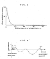
- Waviness is defined as shown in FIG. 6.
- the vertical position of a start point and an end point of measurement that are determined to have the same height is assumed as the origin in the vertical or height direction.
- the absolute values Y 1 to Y 29 of displacement from the origin are measured at intervals of 2 mm.
- the average Y of the absolute values Y 1 to Y 29 represents waviness.
- Alkali etching was first performed under the same conditions as in Example 1 except that the target etching amount was set to 4 ⁇ m, and immediately after the alkali etching, acid etching was performed with a target etching amount being set to 36 ⁇ m. There was not performed a treatment for making the surface of the wafers hydrophilic through use of an aqueous solution of hydrogen peroxide. The results of measurement performed for the thus-etched wafers are shown in Table 1.
- Example 1 Only the alkali etching employed in Example 1 with a target etching amount being set to 20 ⁇ m was performed for wafers. The results of measurement performed for the thus-etched wafers are shown in Table 1.
- Table 1 demonstrates the following.
- Comparative Example 2 Although the flatness of each wafer is good, the surface roughness deteriorates, and especially, the depth of locally formed deep pits increases.
- acid etching is performed after alkali etching (Comparative Example 1), the flatness of wafer becomes considerably worse because of the large acid etching amount.
- alkali etching and acid etching are performed with their etching amounts being properly set (Example 1), well-balanced results are obtained in terms of flatness, surface roughness, and depth of deep pits.
- observation of the surface shape through use of a microscope reveals that the wafers obtained in Example 1 have a surface shape smoother than that of the wafers obtained in Comparative Example 2 and as smooth as that of the wafers obtained in Comparative Example 1.
- the following etching treatment was performed for wafers having a diameter of 8 inches that had undergone lapping (#1200 lapping abrasive grains).
- the wafers were immersed in an NaOH aqueous solution (concentration: 50 wt.%) at 85°C for 450 seconds in order to perform alkali etching with a target etching amount being set to 20 ⁇ m. Subsequently, the wafers were dipped into an aqueous solution of 0.3% hydrogen peroxide in order to make the surface of the wafers hydrophilic.
- the etched wafers were measured for flatness, surface roughness, pit depth, and waviness in order to evaluate the effect of etching. The results are shown in Table 1. The results demonstrate that the reaction-controlled acid etching is especially effective for improvement of flatness (TTV, LTV max ) and waviness.
- Alkali etching and reaction-controlled acid etching were performed under same conditions as in Example 2 for 8-inch wafers that undergone lapping through combined use of #1200 abrasive grains and #1500 abrasive grains.
- the etched wafers were measured for flatness, surface roughness, pit depth, and waviness in order to evaluate the effect of etching.
- the results are shown in Table 1.
- the results obtained in this example demonstrate that the reaction-controlled acid etching is especially effective for improvement of flatness (TTV, LTV max ) and waviness.
- the following etching treatment was performed for wafers having a diameter of 8 inches that had undergone lapping (#1200 lapping abrasive grains).
- the etched wafers were measured for flatness, surface roughness, pit depth, and waviness in order to evaluate the effect of etching. The results are shown in Table 2.
- Etching amount of the reaction-controlled acid etching (target value: 20 ⁇ m): number of samples: 50, average value: 20.1 ⁇ m, average value ⁇ 3 ⁇ : 18.1 - 22.1 ⁇ m.
- Etching amount of the diffusion-controlled acid etching (target value: 10 ⁇ m): number of samples: 50, average value: 9.8 ⁇ m, average value ⁇ 3 ⁇ : 8.3 - 11.3 ⁇ m.
- TTV Flatness
- LTV flatness measuring device
- Surface roughness (Ra) was measured by use of a universal surface shape measuring device (Type: SE-3C, product of Kosaka Laboratory Co.).
- Reaction-controlled acid etching was first performed under the same conditions as in Example 4 except that the target etching amount was set to 4 ⁇ m, and immediately after the reaction-controlled acid etching, diffusion-controlled acid etching was performed with a target etching amount being set to 26 ⁇ m.
- the results of measurement performed for the thus-etched wafers are shown in Table 2.
- Wafers were subjected to only the reaction-controlled acid etching employed in Example 4 with a target etching amount being set to 30 ⁇ m.
- the results of measurement performed for the thus-etched wafers are shown in Table 2.
- Table 2 demonstrates the following.
- reaction-controlled acid etching is performed (Comparative Example 4)
- the flatness of wafer is good, the surface roughness deteriorates, and especially, the depth of locally formed deep pits increases.
- diffusion-controlled acid etching is performed after reaction-controlled acid etching (Comparative Example 3)
- the etching amount of the diffusion-controlled acid etching is excessive, so that the flatness of wafer deteriorates considerably.
- reaction-controlled acid etching and diffusion-controlled acid etching are performed with their etching amounts being properly set (Example 4)
- well-balanced results are obtained in terms of flatness, surface roughness, and depth of deep pits.
- observation of the surface shape through use of a microscope reveals that the wafers obtained in Example 4 have a surface shape smoother than that of the wafers obtained in Comparative Example 4 and as smooth as that of the wafers obtained in Comparative Example 3.
- the present invention is not limited to the above-described embodiment.
- the above-described embodiment is a mere example, and those having the substantially same structure as that described in the appended claims and providing the similar action and effects are included in the scope of the present invention.
- additives such as surfactants may be added to the alkali etchants and the acid etchants used in the above-described embodiments. More specifically, when nitrite such as NaNO 2 is added to the alkali etchant, the depth of pits can be reduced more effectively. When a fluorine-contained or nonionic surfactant is added to the acid etchant, generation of stain can be reduced more effectively.
- a mixed acid aqueous solution composed of hydrofluoric acid, nitric acid, acetic acid, and water is described as an example of the acid etchant.
- similar effects are attained even when there is used a mixed acid aqueous solution composed of hydrofluoric acid, nitric acid, and water but does not contain acetic acid.
- an etchant obtained through dissolution of silicon into a mixed acid aqueous solution composed of hydrofluoric acid, nitric acid, acetic acid, and water is described an example of the etchants used in the reaction-controlled acid etching and the diffusion-controlled acid etching.
- the present invention can be applied to the case where there is used an etchant obtained through addition of acetic acid, phosphoric acid, or sulfuric acid into a three-component mixed acid aqueous solution composed of hydrofluoric acid, nitric acid, and water.
- the present invention is not limited thereto and can be applied to wafers of other semiconductor material such as a compound semiconductor (e.g., Ge, GaAs, Gap, InP).
- a compound semiconductor e.g., Ge, GaAs, Gap, InP.
Landscapes
- Engineering & Computer Science (AREA)
- Microelectronics & Electronic Packaging (AREA)
- Condensed Matter Physics & Semiconductors (AREA)
- General Physics & Mathematics (AREA)
- Manufacturing & Machinery (AREA)
- Computer Hardware Design (AREA)
- Physics & Mathematics (AREA)
- Power Engineering (AREA)
- Chemical & Material Sciences (AREA)
- Chemical Kinetics & Catalysis (AREA)
- General Chemical & Material Sciences (AREA)
- Mechanical Treatment Of Semiconductor (AREA)
- Weting (AREA)
Applications Claiming Priority (7)
| Application Number | Priority Date | Filing Date | Title |
|---|---|---|---|
| JP35615397 | 1997-12-09 | ||
| JP35615397 | 1997-12-09 | ||
| JP12285898A JP3491523B2 (ja) | 1998-04-15 | 1998-04-15 | 半導体ウエーハの加工方法 |
| JP12285898 | 1998-04-15 | ||
| JP24110198A JP3441979B2 (ja) | 1997-12-09 | 1998-08-11 | 半導体ウエーハの加工方法および半導体ウエーハ |
| JP24110198 | 1998-08-11 | ||
| EP98310071.0A EP0928017B1 (fr) | 1997-12-09 | 1998-12-08 | Procédé de production des plaquettes semi-conductrices |
Related Parent Applications (2)
| Application Number | Title | Priority Date | Filing Date |
|---|---|---|---|
| EP98310071.0A Division EP0928017B1 (fr) | 1997-12-09 | 1998-12-08 | Procédé de production des plaquettes semi-conductrices |
| EP98310071.0A Division-Into EP0928017B1 (fr) | 1997-12-09 | 1998-12-08 | Procédé de production des plaquettes semi-conductrices |
Publications (1)
| Publication Number | Publication Date |
|---|---|
| EP1564796A1 true EP1564796A1 (fr) | 2005-08-17 |
Family
ID=27314533
Family Applications (2)
| Application Number | Title | Priority Date | Filing Date |
|---|---|---|---|
| EP98310071.0A Expired - Lifetime EP0928017B1 (fr) | 1997-12-09 | 1998-12-08 | Procédé de production des plaquettes semi-conductrices |
| EP05010508A Withdrawn EP1564796A1 (fr) | 1997-12-09 | 1998-12-08 | Procédé de production des plaquettes semi-conductrices et plaquettes ainsi obtenues |
Family Applications Before (1)
| Application Number | Title | Priority Date | Filing Date |
|---|---|---|---|
| EP98310071.0A Expired - Lifetime EP0928017B1 (fr) | 1997-12-09 | 1998-12-08 | Procédé de production des plaquettes semi-conductrices |
Country Status (3)
| Country | Link |
|---|---|
| US (3) | US6239039B1 (fr) |
| EP (2) | EP0928017B1 (fr) |
| MY (1) | MY120464A (fr) |
Families Citing this family (25)
| Publication number | Priority date | Publication date | Assignee | Title |
|---|---|---|---|---|
| JP2001085648A (ja) * | 1999-07-15 | 2001-03-30 | Shin Etsu Handotai Co Ltd | 貼り合わせウエーハの製造方法および貼り合わせウエーハ |
| DE19962136A1 (de) * | 1999-12-22 | 2001-06-28 | Merck Patent Gmbh | Verfahren zur Rauhätzung von Siliziumsolarzellen |
| KR100792774B1 (ko) * | 2000-06-29 | 2008-01-11 | 신에쯔 한도타이 가부시키가이샤 | 반도체 웨이퍼의 가공방법 및 반도체 웨이퍼 |
| WO2002003432A2 (fr) * | 2000-06-30 | 2002-01-10 | Memc Electronic Materials, Inc. | Procede de gravure de plaquettes de silicium |
| TW511180B (en) * | 2000-07-31 | 2002-11-21 | Mitsubishi Chem Corp | Mixed acid solution in etching process, process for producing the same, etching process using the same and process for producing semiconductor device |
| US6672943B2 (en) | 2001-01-26 | 2004-01-06 | Wafer Solutions, Inc. | Eccentric abrasive wheel for wafer processing |
| US6632012B2 (en) | 2001-03-30 | 2003-10-14 | Wafer Solutions, Inc. | Mixing manifold for multiple inlet chemistry fluids |
| JP2003086554A (ja) * | 2001-09-11 | 2003-03-20 | Mitsubishi Heavy Ind Ltd | 半導体基板の製造装置、及び、その製造方法 |
| JP2003163335A (ja) * | 2001-11-27 | 2003-06-06 | Shin Etsu Handotai Co Ltd | 貼り合わせウェーハの製造方法 |
| TW200411759A (en) * | 2002-09-18 | 2004-07-01 | Memc Electronic Materials | Process for etching silicon wafers |
| DE10328845B4 (de) * | 2003-06-26 | 2005-10-20 | Siltronic Ag | Verfahren zur Oberflächenbehandlung einer Halbleiterscheibe |
| WO2005036629A1 (fr) * | 2003-10-10 | 2005-04-21 | Mimasu Semiconductor Industry Co., Ltd. | Procede de rugosification de la surface d'une plaquette |
| US7338904B2 (en) * | 2003-12-05 | 2008-03-04 | Sumco Corporation | Method for manufacturing single-side mirror surface wafer |
| JP2005175106A (ja) * | 2003-12-10 | 2005-06-30 | Sumitomo Mitsubishi Silicon Corp | シリコンウェーハの加工方法 |
| JP4700333B2 (ja) * | 2003-12-22 | 2011-06-15 | シルトロニック・ジャパン株式会社 | シリコンウエーハ用の高純度アルカリエッチング液およびシリコンウエーハアルカリエッチング方法 |
| US7247578B2 (en) * | 2003-12-30 | 2007-07-24 | Intel Corporation | Method of varying etch selectivities of a film |
| JP2006100799A (ja) * | 2004-09-06 | 2006-04-13 | Sumco Corp | シリコンウェーハの製造方法 |
| US20060194441A1 (en) * | 2005-02-25 | 2006-08-31 | Sakae Koyata | Method for etching a silicon wafer and method for performing differentiation between the obverse and the reverse of a silicon wafer using the same method |
| JP4835175B2 (ja) * | 2006-01-31 | 2011-12-14 | 株式会社Sumco | ウェーハの枚葉式エッチング方法 |
| US20080202551A1 (en) * | 2006-12-29 | 2008-08-28 | Siltron Inc. | Method for cleaning solar cell substrates |
| JP2010226089A (ja) * | 2009-01-14 | 2010-10-07 | Rohm & Haas Electronic Materials Llc | 半導体ウェハをクリーニングする方法 |
| JP4831216B2 (ja) * | 2009-07-28 | 2011-12-07 | 株式会社Sumco | ウェーハ表面処理方法 |
| CN102956744A (zh) * | 2011-08-29 | 2013-03-06 | 浚鑫科技股份有限公司 | 一种太阳能电池片丝网印刷的方法 |
| CN102592972B (zh) * | 2012-01-19 | 2014-12-31 | 英利能源(中国)有限公司 | 太阳能电池硅片的清洗方法 |
| CN112951716A (zh) * | 2021-03-22 | 2021-06-11 | 上海中欣晶圆半导体科技有限公司 | 一种通过混腐蚀改善平坦度与粗糙度的方法 |
Citations (3)
| Publication number | Priority date | Publication date | Assignee | Title |
|---|---|---|---|---|
| EP0617457A2 (fr) * | 1993-03-24 | 1994-09-28 | Shin-Etsu Handotai Company Limited | Procédé pour fabriquer des disques semi-conducteurs |
| EP0754785A1 (fr) * | 1995-07-21 | 1997-01-22 | Shin-Etsu Handotai Company Limited | Procédé de fabrication de plaquettes semi-conductrices avec surface polie comme une glace |
| EP0774776A2 (fr) * | 1995-10-03 | 1997-05-21 | KABUSHIKI KAISHA KOBE SEIKO SHO also known as Kobe Steel Ltd. | Procédé de recupération de substrats |
Family Cites Families (7)
| Publication number | Priority date | Publication date | Assignee | Title |
|---|---|---|---|---|
| DE4316096C1 (de) * | 1993-05-13 | 1994-11-10 | Wacker Chemitronic | Verfahren zur naßchemischen Behandlung scheibenförmiger Werkstücke |
| JP2836570B2 (ja) | 1996-03-28 | 1998-12-14 | 日本電気株式会社 | 半導体記憶装置 |
| JPH09266194A (ja) | 1996-03-28 | 1997-10-07 | Shin Etsu Handotai Co Ltd | 半導体ウエーハのエッチング方法 |
| JPH1092777A (ja) * | 1996-09-12 | 1998-04-10 | Komatsu Electron Metals Co Ltd | 半導体ウェハの製造方法 |
| JP3620683B2 (ja) * | 1996-12-27 | 2005-02-16 | 信越半導体株式会社 | 半導体ウエーハの製造方法 |
| JP3305610B2 (ja) * | 1997-02-21 | 2002-07-24 | 信越半導体株式会社 | ラッピング後の半導体ウエーハの洗浄方法 |
| MY119304A (en) * | 1997-12-11 | 2005-04-30 | Shinetsu Handotai Kk | Silicon wafer etching method and silicon wafer etchant |
-
1998
- 1998-12-08 EP EP98310071.0A patent/EP0928017B1/fr not_active Expired - Lifetime
- 1998-12-08 EP EP05010508A patent/EP1564796A1/fr not_active Withdrawn
- 1998-12-08 MY MYPI98005530A patent/MY120464A/en unknown
- 1998-12-08 US US09/207,193 patent/US6239039B1/en not_active Expired - Lifetime
-
2000
- 2000-08-07 US US09/633,401 patent/US6346485B1/en not_active Expired - Fee Related
-
2001
- 2001-02-07 US US09/778,679 patent/US6432837B2/en not_active Expired - Fee Related
Patent Citations (3)
| Publication number | Priority date | Publication date | Assignee | Title |
|---|---|---|---|---|
| EP0617457A2 (fr) * | 1993-03-24 | 1994-09-28 | Shin-Etsu Handotai Company Limited | Procédé pour fabriquer des disques semi-conducteurs |
| EP0754785A1 (fr) * | 1995-07-21 | 1997-01-22 | Shin-Etsu Handotai Company Limited | Procédé de fabrication de plaquettes semi-conductrices avec surface polie comme une glace |
| EP0774776A2 (fr) * | 1995-10-03 | 1997-05-21 | KABUSHIKI KAISHA KOBE SEIKO SHO also known as Kobe Steel Ltd. | Procédé de recupération de substrats |
Also Published As
| Publication number | Publication date |
|---|---|
| EP0928017A2 (fr) | 1999-07-07 |
| US20010008807A1 (en) | 2001-07-19 |
| US6346485B1 (en) | 2002-02-12 |
| EP0928017B1 (fr) | 2014-09-10 |
| US6432837B2 (en) | 2002-08-13 |
| MY120464A (en) | 2005-10-31 |
| EP0928017A3 (fr) | 2003-07-02 |
| US6239039B1 (en) | 2001-05-29 |
Similar Documents
| Publication | Publication Date | Title |
|---|---|---|
| US6239039B1 (en) | Semiconductor wafers processing method and semiconductor wafers produced by the same | |
| EP0798766B1 (fr) | Méthode de formation d'une plaquette semiconductrice monocristalline avec surface à fini mirroir comprenant des étapes d'attaque en phase gazeuse et de chauffage, et plaquettes formées par cette méthode | |
| KR100701342B1 (ko) | 접합 웨이퍼의 제조방법 및 접합 웨이퍼 | |
| EP1450396A1 (fr) | Procede de production d'une tranche de silicone, tranche de silicone et tranche soi | |
| KR20040029292A (ko) | 접합 웨이퍼의 제조방법 | |
| KR100706683B1 (ko) | 실리콘 웨이퍼의 가공 방법 | |
| JP3446616B2 (ja) | シリコンウエーハのエッチング方法およびシリコンウエーハ用エッチング液 | |
| US5899744A (en) | Method of manufacturing semiconductor wafers | |
| KR20000023446A (ko) | 에피택셜웨이퍼 및 그 제조방법 및 그것에 사용되는화합물반도체기판의 표면청정화방법 | |
| EP0860864A2 (fr) | Procédé de nettoyage de substrats semiconducteurs après rodage | |
| US6600557B1 (en) | Method for the detection of processing-induced defects in a silicon wafer | |
| JP3943869B2 (ja) | 半導体ウエーハの加工方法および半導体ウエーハ | |
| JP3441979B2 (ja) | 半導体ウエーハの加工方法および半導体ウエーハ | |
| JPH10335304A (ja) | 半導体ウエハエッチング方法 | |
| KR20040060990A (ko) | 접합 웨이퍼의 제조 방법 | |
| JP2001085648A (ja) | 貼り合わせウエーハの製造方法および貼り合わせウエーハ | |
| JP3503444B2 (ja) | 半導体ウエーハのエッチング工程を有する半導体ウエーハの製造方法 | |
| JP2003007672A (ja) | シリコン半導体ウェーハのエッチング方法 | |
| JP3522475B2 (ja) | シリコンウェーハ表面粗さ制御用のエッチャント | |
| JP3491523B2 (ja) | 半導体ウエーハの加工方法 | |
| EP2090675B1 (fr) | Gravure de défauts de germanium | |
| JP4075426B2 (ja) | シリコンウェーハの製造方法 | |
| JP3890981B2 (ja) | アルカリエッチング液及びこのエッチング液を用いたシリコンウェーハのエッチング方法並びにこの方法を用いたシリコンウェーハの表裏面差別化方法 | |
| WO2023032488A1 (fr) | Procédé de nettoyage de tranche de silicium et procédé de production de tranche de silicium | |
| CN116581220A (zh) | 表面粗糙化方法 |
Legal Events
| Date | Code | Title | Description |
|---|---|---|---|
| PUAI | Public reference made under article 153(3) epc to a published international application that has entered the european phase |
Free format text: ORIGINAL CODE: 0009012 |
|
| AC | Divisional application: reference to earlier application |
Ref document number: 0928017 Country of ref document: EP Kind code of ref document: P |
|
| AK | Designated contracting states |
Kind code of ref document: A1 Designated state(s): DE IT |
|
| 17P | Request for examination filed |
Effective date: 20051222 |
|
| AKX | Designation fees paid |
Designated state(s): DE IT |
|
| STAA | Information on the status of an ep patent application or granted ep patent |
Free format text: STATUS: THE APPLICATION IS DEEMED TO BE WITHDRAWN |
|
| 18D | Application deemed to be withdrawn |
Effective date: 20080701 |