EP1559812B1 - Verfahren zur bestimmung derpunktdefektverteilung eines siliciumeinkristallstabs - Google Patents
Verfahren zur bestimmung derpunktdefektverteilung eines siliciumeinkristallstabs Download PDFInfo
- Publication number
- EP1559812B1 EP1559812B1 EP03756681A EP03756681A EP1559812B1 EP 1559812 B1 EP1559812 B1 EP 1559812B1 EP 03756681 A EP03756681 A EP 03756681A EP 03756681 A EP03756681 A EP 03756681A EP 1559812 B1 EP1559812 B1 EP 1559812B1
- Authority
- EP
- European Patent Office
- Prior art keywords
- sample
- region
- transition metal
- concentration
- measurement
- Prior art date
- Legal status (The legal status is an assumption and is not a legal conclusion. Google has not performed a legal analysis and makes no representation as to the accuracy of the status listed.)
- Expired - Lifetime
Links
Images






Classifications
-
- C—CHEMISTRY; METALLURGY
- C30—CRYSTAL GROWTH
- C30B—SINGLE-CRYSTAL GROWTH; UNIDIRECTIONAL SOLIDIFICATION OF EUTECTIC MATERIAL OR UNIDIRECTIONAL DEMIXING OF EUTECTOID MATERIAL; REFINING BY ZONE-MELTING OF MATERIAL; PRODUCTION OF A HOMOGENEOUS POLYCRYSTALLINE MATERIAL WITH DEFINED STRUCTURE; SINGLE CRYSTALS OR HOMOGENEOUS POLYCRYSTALLINE MATERIAL WITH DEFINED STRUCTURE; AFTER-TREATMENT OF SINGLE CRYSTALS OR A HOMOGENEOUS POLYCRYSTALLINE MATERIAL WITH DEFINED STRUCTURE; APPARATUS THEREFOR
- C30B33/00—After-treatment of single crystals or homogeneous polycrystalline material with defined structure
-
- C—CHEMISTRY; METALLURGY
- C04—CEMENTS; CONCRETE; ARTIFICIAL STONE; CERAMICS; REFRACTORIES
- C04B—LIME, MAGNESIA; SLAG; CEMENTS; COMPOSITIONS THEREOF, e.g. MORTARS, CONCRETE OR LIKE BUILDING MATERIALS; ARTIFICIAL STONE; CERAMICS; REFRACTORIES; TREATMENT OF NATURAL STONE
- C04B24/00—Use of organic materials as active ingredients for mortars, concrete or artificial stone, e.g. plasticisers
- C04B24/003—Phosphorus-containing compounds
-
- C—CHEMISTRY; METALLURGY
- C04—CEMENTS; CONCRETE; ARTIFICIAL STONE; CERAMICS; REFRACTORIES
- C04B—LIME, MAGNESIA; SLAG; CEMENTS; COMPOSITIONS THEREOF, e.g. MORTARS, CONCRETE OR LIKE BUILDING MATERIALS; ARTIFICIAL STONE; CERAMICS; REFRACTORIES; TREATMENT OF NATURAL STONE
- C04B28/00—Compositions of mortars, concrete or artificial stone, containing inorganic binders or the reaction product of an inorganic and an organic binder, e.g. polycarboxylate cements
- C04B28/14—Compositions of mortars, concrete or artificial stone, containing inorganic binders or the reaction product of an inorganic and an organic binder, e.g. polycarboxylate cements containing calcium sulfate cements
- C04B28/145—Calcium sulfate hemi-hydrate with a specific crystal form
- C04B28/146—Calcium sulfate hemi-hydrate with a specific crystal form alpha-hemihydrate
-
- C—CHEMISTRY; METALLURGY
- C30—CRYSTAL GROWTH
- C30B—SINGLE-CRYSTAL GROWTH; UNIDIRECTIONAL SOLIDIFICATION OF EUTECTIC MATERIAL OR UNIDIRECTIONAL DEMIXING OF EUTECTOID MATERIAL; REFINING BY ZONE-MELTING OF MATERIAL; PRODUCTION OF A HOMOGENEOUS POLYCRYSTALLINE MATERIAL WITH DEFINED STRUCTURE; SINGLE CRYSTALS OR HOMOGENEOUS POLYCRYSTALLINE MATERIAL WITH DEFINED STRUCTURE; AFTER-TREATMENT OF SINGLE CRYSTALS OR A HOMOGENEOUS POLYCRYSTALLINE MATERIAL WITH DEFINED STRUCTURE; APPARATUS THEREFOR
- C30B15/00—Single-crystal growth by pulling from a melt, e.g. Czochralski method
-
- C—CHEMISTRY; METALLURGY
- C30—CRYSTAL GROWTH
- C30B—SINGLE-CRYSTAL GROWTH; UNIDIRECTIONAL SOLIDIFICATION OF EUTECTIC MATERIAL OR UNIDIRECTIONAL DEMIXING OF EUTECTOID MATERIAL; REFINING BY ZONE-MELTING OF MATERIAL; PRODUCTION OF A HOMOGENEOUS POLYCRYSTALLINE MATERIAL WITH DEFINED STRUCTURE; SINGLE CRYSTALS OR HOMOGENEOUS POLYCRYSTALLINE MATERIAL WITH DEFINED STRUCTURE; AFTER-TREATMENT OF SINGLE CRYSTALS OR A HOMOGENEOUS POLYCRYSTALLINE MATERIAL WITH DEFINED STRUCTURE; APPARATUS THEREFOR
- C30B29/00—Single crystals or homogeneous polycrystalline material with defined structure characterised by the material or by their shape
- C30B29/02—Elements
- C30B29/06—Silicon
-
- C—CHEMISTRY; METALLURGY
- C04—CEMENTS; CONCRETE; ARTIFICIAL STONE; CERAMICS; REFRACTORIES
- C04B—LIME, MAGNESIA; SLAG; CEMENTS; COMPOSITIONS THEREOF, e.g. MORTARS, CONCRETE OR LIKE BUILDING MATERIALS; ARTIFICIAL STONE; CERAMICS; REFRACTORIES; TREATMENT OF NATURAL STONE
- C04B2111/00—Mortars, concrete or artificial stone or mixtures to prepare them, characterised by specific function, property or use
- C04B2111/00474—Uses not provided for elsewhere in C04B2111/00
- C04B2111/00836—Uses not provided for elsewhere in C04B2111/00 for medical or dental applications
-
- Y—GENERAL TAGGING OF NEW TECHNOLOGICAL DEVELOPMENTS; GENERAL TAGGING OF CROSS-SECTIONAL TECHNOLOGIES SPANNING OVER SEVERAL SECTIONS OF THE IPC; TECHNICAL SUBJECTS COVERED BY FORMER USPC CROSS-REFERENCE ART COLLECTIONS [XRACs] AND DIGESTS
- Y10—TECHNICAL SUBJECTS COVERED BY FORMER USPC
- Y10T—TECHNICAL SUBJECTS COVERED BY FORMER US CLASSIFICATION
- Y10T117/00—Single-crystal, oriented-crystal, and epitaxy growth processes; non-coating apparatus therefor
- Y10T117/10—Apparatus
- Y10T117/1004—Apparatus with means for measuring, testing, or sensing
- Y10T117/1008—Apparatus with means for measuring, testing, or sensing with responsive control means
Definitions
- the present invention relates to a method for measuring the defect distribution of intrinsic point defect which is formed in a silicon single crystal ingot (hereinafter, referred to as an ingot), or a p-type silicon single crystal ingot (hereinafter, referred to as a p-type ingot) which is pulled up by a Czochralski method (hereinafter, referred to as the CZ method). More specifically, the present invention relates to a method of evaluating the defect distribution of intrinsic point defect of a silicon wafer which makes the production of a no defects region silicon wafer easy.
- COP crystal originated particle
- OISF nucleus of oxidation induced stacking fault
- L/D interstitial-type large dislocation
- the COP is a pit originated in a crystal which appears on the surface of a wafer when a silicon wafer which is polished in mirror surface is rinsed by the SC-1 method with a mixed solution of ammonia and hydrogen peroxide.
- LPD Light Point Defect
- the COP is a cause for deteriorating electric properties such as, for example, the time dependent dielectric breakdown (TDDB) of an oxide film and the time zero dielectric breakdown (TZDB) of an oxide film.
- TDDB time dependent dielectric breakdown
- TZDB time zero dielectric breakdown
- a minute oxygen precipitation which is formed at crystal growth is the nucleus of OISF, and the OISF is a stacking defect which is exposed at a thermal oxidation step when a semiconductor device is produced.
- the OISF becomes the cause of trouble of increasing the leak current of the device, and the like.
- the L/D is also called as dislocation cluster, or also called as dislocation pit because when a silicon wafer generating the defect is immersed in a selective etching solution in which fluoric acid is a main component, etching pit having orientation is generated.
- the L/D is also a cause of deteriorating electric properties such as, for example, leak property and isolation property.
- a defect-free ingot having no COP, OISF and L/D and a silicon wafer which is sliced from the ingot are disclosed in JP-A-11-1393 corresponding to US Patent No. 6,045,610 .
- the defect-free ingot is an ingot comprising a perfect region [P] when the perfect region in which a agglomerate of vacancy type point defects and interstitial silicon type point defects in the ingot are respectively not detected is referred to as [P].
- the perfect region [P] exists between a region [V] having defects where the vacancy type point defect is dominant in an ingot and excessively saturated vacancies are agglomerated and a region [I] having defects where the interstitial silicon type point defect is dominant and excessively saturated interstitial silicons are agglomerated.
- the perfect region [P] having no defect where the point defects are agglomerated is classified into a region [Pv] where the vacancy type point defect is dominant and a region [Pi] where the interstitial silicon type point defect is dominant.
- the [Pv] region is adjacent to the [V] region and a region having a concentration of vacancy type point defect which is less than the minimum concentration of vacancy type point defect which can form a OISF nuclei.
- the [Pi] region is adjacent to the [I] region and a defect region having a concentration of interstitial silicon type point defect which is less than the minimum concentration of interstitial silicon type point defect which can form an interstitial-type dislocation.
- an ingot comprising the perfect region [P] is prepared within a range of V/G (mm 2 /min.°C) in a region where OISF (P band) which is generated in a ring form at thermal oxidation processing is extinguished at the center of a wafer and L/D (B band) is not generated.
- a silicon single crystal ingot is prepared at a condition by which a defect-free region is formed, for evaluation of the concentration distribution of point defect to an axial direction and a diameter direction.
- a sample is prepared by slicing the ingot to an axial direction.
- the sample is mirror-etched, it is thermally treated at 800°C for 4 hours under nitrogen or oxidative atmosphere and thermally treated at 1000°C for 16 hours, successively.
- the sample thermally treated is measured by measurement methods such as the copper-decoration, the secco-etching, the X-ray topography and the lifetime measurement. As shown in FIGS. 23 and 24 , since oxygen precipitate appears in the ingot by the above-mentioned thermal treatment, respective region and respective boundary have been discriminated and judged from the oxygen precipitates.
- FIG.23 is a chart showing the in-plane distribution of recombination lifetime when the thermal heat treatment for oxygen precipitation is carried out for a sample containing the regions [V], [Pv], [Pi] and [I] which is prepared by changing the pulling-up speed from a high speed to a low speed by a crystal pulling-up apparatus having a hot zone which can prepare a defect-free silicon single crystal ingot
- FIG. 24 is a chart showing the recombination lifetime in the A-A line section of FIG. 23 .
- the measurement value of recombination lifetime is remarkably dependent on the oxygen concentration in a sample and the thermal heat treatment for oxygen precipitation condition.
- the concentration of oxygen dissolved in an ingot is low, the density of the oxygen precipitate which is formed by the thermal heat treatment for oxygen precipitation is low in comparison with a sample in which the concentration of dissolved oxygen is high; therefore the difference value of the recombination lifetimes becomes small.
- thermal treatment for a long time is not only required for the thermal heat treatment for oxygen precipitation, but also the condition of the thermal treatment affects the oxygen precipitation in an ingot; therefore the boundary region of the point defect regions is shifted to either region side of the region [Pv] or the region [Pi]. Consequently, it is difficult to discriminate and judge the original point defect region.
- GB - A - 2 324 652 relates to a method of analyzing crystal defects of bare wafers using thermal treatment processes.
- the invention according to Claim 1 is a method for measuring the point defect distribution of a silicon single crystal ingot, comprising
- the regions [Pi] and [I] and boundary thereof are specified with high precision and a short time without depending on the concentration of oxygen dissolved in an ingot, by combining the recombination lifetime distribution of the first transition metal which specifies the boundary of the regions [V] and [Pv] with high precision, with the recombination lifetime distribution of the second transition metal which specifies the boundary of the regions [Pi] and [I] with high precision.
- the invention according to Claim 2 is the invention according to claim 1, wherein the measurement method further comprises after the step (g1),
- the regions [Pv] and [Pi] and boundary thereof are specified with high precision and a short time without depending on the concentration of oxygen dissolved in an ingot from the combined recombination lifetime distributions and the two correlation straight lines, by combining the recombination lifetime distribution of the first transition metal with the recombination lifetime distribution of the second transition metal, and further, respectively preparing the correlation straight line from the metal concentration of the first transition metal and the recombination lifetime distribution of the first transition metal and similarly, the correlation straight line from the metal concentration of the second transition metal and the recombination lifetime distribution of the second transition metal.
- the invention according to Claim 3 is the invention according to Claim 1 and the measurement method wherein the first transition metal is Cu or Fe and the second transition metal is Ni or Co.
- the invention according to Claim 4 is the invention according to Claim 2 and the measurement method wherein the first transition metal is Cu and the second transition metal is Fe.
- the invention according to Claim 5 is the invention according to Claim 1 or 2, and the measurement method wherein the diffusion thermal treatment step of the first and second transition metals in the step (e1) is a thermal treatment at 600°C to 1150°C for 0.5 hour to 24 hours.
- the invention according to Claim 6 is the invention according to Claim 1 or 2 and the measurement method wherein the measurement of the recombination lifetime in the step (f1) is measured using the LM-PCD (laser/microwave photoconductance decay method).
- LM-PCD laser/microwave photoconductance decay method
- the invention according to Claim 7 is the invention according to Claim 1 or 3 and the measurement method, further comprising a step of selectively etching the surface of the second sample which is thermally treated with the step (e1) when the second transition metal with which the second sample is metal-stained is Ni.
- nickel silicide is formed on the surface of the sample by carrying out diffusion thermal treatment to the second sample.
- nickel silicide is formed, in the following recombination lifetime measurement step, surface recombination speed is increased and there is generated a problem that an accurate value cannot be measured. Consequently, nickel silicide is removed by selectively etching the surface of the sample.
- the regions [Pv] and [Pi] and boundary thereof are specified with high precision and a short time without depending on the concentration of oxygen dissolved in an ingot, by using the high temperature dependency of dissolution thermal treatment of the transition metal M.
- the transition metal M is Fe
- the minor carrier diffusion lengths in the steps (g3) and (f3) are measured using the SPV (surface photo-voltage method).
- the concentration of recombination center of the transition metal M in the step (f3) is measured using the DLTS (deep level transient spectroscopy).
- the ingot being the objective of the measurement method of the present invention is pulled up from silicon melt by controlling a V/G ratio so as to include the regions [V], [Pv], [Pi] and [I].
- the ingot is an ingot in which its oxygen concentration is a range of 8.0 ⁇ 10 17 atoms/cm 3 to 1.0 ⁇ 10 18 atoms/cm 3 (old ASTM, hereinafter, it is the same), or the boundary of the regions [Pv] and [Pi] in a sample which is obtained by slicing the ingot to be thermally treated at 800°C for 4 hours under nitrogen atmosphere, successively, thermally treated at 1000°C for 16 hours and then in which the recombination lifetime is measured, cannot be identified.
- the ingot being the objective of the above described, not claimed measurement method is pulled up from silicon melt doped with boron, by controlling a V/G ratio so as to include the regions [V], [Pv], [Pi] and [I].
- the ingot is pulled up from silicon melt in a hot zone furnace based on the theory of Voronkov by the CZ method or the magnetic field applied CZ method.
- point defect and the agglomerate of point defects are generated as defects in the silicon single crystal.
- the vacancy type point defect is a defect in which one silicon atom is separated from one of normal positions in a silicon crystal lattice. Such vacancies are agglomerated to form the vacancy type defect.
- interstitial silicons are agglomerated to form the interstitial silicon type defect.
- the point defect is generally introduced at a contact plane between silicon melt (melted silicon) and an ingot (solid silicon). However, when the ingot is continuously pulled up, a portion which is the contact plane is cooled in accordance with pulling-up.
- the vacancy or the interstitial silicon carries out diffusion and pair annihilation reaction during cooling.
- Excessive point defects at the time of cooling until about 1100°C form the agglomerates of the vacancy type point defects (vacancy agglomerates) or the agglomerates of the interstitial silicon type point defects (interstitial agglomerates). In other word, they are three dimensional structures which the excessive point defects form agglomerates and generate.
- the vacancy agglomerates include defects called as LSTD (Laser Scattering Tomograph Defects) or FPD (Flow Pattern Defects) in addition to the fore-mentioned COP, and the interstitial agglomerates include the fore-mentioned defect called as L/D.
- LSTD is a source which has a refractive index different from silicon, and which generate scattered light when infrared ray is irradiated into a silicon single crystal.
- Voronkov is that when the pulling-up speed of an ingot is set as V (mm/min.) and when the temperature gradient nearby solid-liquid interface between silicon melt and a silicon ingot is set as G (°C/mm), V/G (mm 2 /min.°C) is controlled in order to grow a high purity ingot with little number of defect.
- V/G mm 2 /min.°C
- FIG.2 the relation between V/G and a point defect concentration is schematically represented by setting V/G as a horizontal axis and setting the concentration of the vacancy type point defects and the concentration of the interstitial silicon type point defects as the same longitudinal axis, and the theory explains the boundary between a vacancy region and an interstitial silicon region is determined by V/G.
- V/G ratio is a critical point (V/G) c or more, an ingot in which the concentration of vacancy is raised is formed, and to the contrary, when the V/G ratio is the critical point (V3) c or less, an ingot in which the concentration of interstitial silicon is raised is formed.
- [I] indicates a region ((V/G) 1 or less) having defects where the interstitial silicon is dominant and interstitial silicons are agglomerated
- [V] indicate a region ((V/G) 2 or more) having defects where vacancy is dominant and vacancies are agglomerated
- [P] indicates a perfect region ((V/G) 1 to (V/G) 2 ) where the vacancy agglomerates and the interstitial agglomerates do not exist.
- a P band region ((V/G) 2 to (V/G) 3 ) forming the OISF nucleus exists at the boundary with the region [V] at a side adjacent to the region [P].
- a B band region ((V/G) 4 to (V/G) 1 ) exists at the boundary of the region [I] at a side adjacent to the region [P].
- the B band region is a region in which the agglomerate of the interstitial silicons becomes nucleus and oxygen precipitation is generated at a high concentration by thermal treatment.
- the perfect region [P] is further classified into a region [Pi] and a region [Pv].
- [Pi] is a region in which the V/G ratio is from the above-mentioned (V/G) 1 to the critical point and a region having defects in which the interstitial silicon is dominant and interstitial silicons are not agglomerated.
- [Pv] is a region in which the V/G ratio is from the critical point to the above-mentioned (V/G) 2 and a region having defects in which the vacancy is dominant and vacancies are not agglomerated.
- [Pi] is adjacent to the region [I] and a region having the concentration of interstitial silicon which is less than the minimum concentration of interstitial silicon which can form interstitial dislocation
- [Pv] is adjacent to the region [V] and a region having the concentration of vacancy which is less than the minimum concentration of vacancy which can form OISF nucleus.
- the ingot being the objective of the measurement method of the present invention is pulled up by being controlled so that the V/G ratio includes respective regions from the above-mentioned (V/G) 4 or less to the critical point and (V/G) 3 or more, in order to include the regions [V], [Pv], [Pi] and [I].
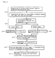
- FIGS.1 and 3 the first embodiment of the measurement method of the present invention is illustrated based on FIGS.1 and 3 .
- a sample for measurement is prepared from a test ingot (step (a1)). Namely, an ingot is pulled up from silicon melt which is stored in the quartz crucible of a pulling-up device based on the CZ method or the magnetic field applied CZ method. At this time, the ingot is pulled up by changing the pulling-up speed V (mm/min.) of the ingot from a high speed (top side) to a low speed (bottom side), or a low speed (bottom side) to a high speed (top side) so that the above-mentioned regions [V], [Pv], [Pi] and [I] are contained to the axis direction of the ingot.
- V pulling-up speed
- a sample for measurement having a thickness of 500 to 2000 ⁇ m whose surface is mirror-polished is prepared by cutting the ingot obtained in the test so as to include the central axis of the ingot to axis direction and by carrying out mirror-etching ( FIGS.3(a) and 3(b) ).
- Each of the regions [V], [Pv], [Pi]and [I] is contained in the sample for measurement.
- the ingot shown in FIG.3 is an ingot pulled up by changing the pulling-up speed V (mm/min.) from a high speed (top side) to a low speed (bottom side).
- the concentration of oxygen dissolved in the sample for measurement is measured by the FT-IR (Fourier transform infrared absorption spectroscopy) method, and when the concentration of oxygen is 1.0 ⁇ 10 18 atoms/cm 3 or more, the sample is thermally treated at 800°C for 4 hours and successively, thermally treated at 1000°C for 16 hours, under nitrogen atmosphere.
- the recombination lifetime of the sample for measurement thermally treated is measured over the whole sample by the LM-PCD method.
- FIG.23 is one example of the measurement result. As shown in FIG.23 , oxygen precipitate appeared in the sample in high density by the above-mentioned thermal treatment.
- the regions [V], [Pv], [Pi] and [I] are identified for the whole sample in accordance with concentration distribution of oxygen precipitate.
- the P band region forming OISF nucleus exists in the region [V] and the B band region exists in the region [I].
- the concentration of oxygen of the sample for measurement is less than 1.0 ⁇ 10 18 atoms/cm 3 , even if the sample for measurement is thermally treated in like manner as the above-description and the recombination lifetime of the sample for measurement is measured, it cannot be identified from the measurement result of the recombination lifetime whether the perfect region [P] is the region [Pv] or the region [Pi], as shown in FIG.5 .
- the sample for measurement is divided into two so as to be symmetrical against the central axis of the ingot at a position shown in the arrow mark of FIG.3(b) (step (b1)).
- the samples for measurement which are divided according to the above-mentioned step (b1) are set as a first sample and a second sample as shown in FIG.3(c) .
- a first transition metal solution in which a first transition metal is dissolved at a concentration of 1 to 1000 ppm is coated on the surface of the first sample to stain the first sample with the metal (step (c1)).
- the first transition metal is preferably Cu or Fe.
- the first transition metal solution is a solution in which the first transition metal is dissolved at a concentration of 1 to 1000 ppm and preferably 1 to 100 ppm.
- a standard solution for atomic absorption in which Cu or Fe is dissolved at a concentration of 10 to 100 ppm is preferred because of availability and superiority in concentration precision.
- the coating method includes the spin coat method, the dipping method and the like.
- the concentration of the first transition metal is less than the lower limit value, the boundaries of respective regions cannot be adequately identified and the recombination lifetime cannot be measured in high precision. Further, when it exceeds the upper limit value, the transition metal is diffused on the surface and rear face of the sample and forms metal silicide (precipitate) nearby the surface and rear face; therefore recombination center which is a deep energy level cannot be formed in the inside (in crystal) of the sample.
- a second transition metal solution in which a second transition metal different from the first transition metal is dissolved at a concentration of 1 to 1000 ppm is coated on the surface of the second sample to stain the second sample with the metal (step (d1)).
- the second transition metal is preferably Ni or Co.
- the second transition metal solution is a solution in which the second transition metal is dissolved at a concentration of 1 to 1000 ppm and preferably 1 to 100 ppm.
- a standard solution for atomic absorption in which Ni or Co is dissolved at a concentration of 10 to 100 ppm is preferred because of availability and superiority in concentration precision.
- As the coaling method a similar method as the above-mentioned coating method of the first transition metal is used.
- the concentration of the second transition metal is less than the lower limit value, the boundaries of respective regions cannot be adequately identified and the recombination lifetime cannot be measured in high precision. Further, when it exceeds the upper limit value, the transition metal is diffused on the surface and rear face of the sample and forms metal silicide (precipitate) nearby the surface and rear face; therefore recombination center which is a deep energy level cannot be formed in the inside (in crystal) of the sample.
- the first and second samples are thermally treated at 600°C to 1150°C for 0.5 hour to 30 hours under argon, nitrogen, oxygen, hydrogen or mixed gas atmosphere thereof and the first and second transition metals which are respectively coated on the surface of the first and second samples are diffused into the whole samples (step (e1)).
- temperature is raised at a speed of 0.5 to 10°C/min. and thermal treatment is carried out at 600°C to 1150°C for 0.5 hour to 30 hours and preferably for 0.5 hour to 24 hours. It is more preferable that temperature is raised at a speed of 5 to 10°C/min. and thermal treatment is carried out at 900°C to 1000°C for 1 hour to 2 hours.
- the transition metal When the time and temperature of the thermal treatment is less than the lower limit value, the transition metal is not adequately diffused. Further, when they exceed the upper limit value, the transition metal is diffused on the surface and rear face of the sample and forms metal silicide (precipitate) nearby the surface and rear face; therefore recombination center which is a deep energy level cannot be formed in the inside (in crystal) of the sample.
- the second transition metal with which the second sample was stained was Ni
- the recombination lifetime of the second sample thermally treated was measured, as shown in FIG.5
- the recombination lifetimes of the regions [Pi] and [I] were not adequately increased and the boundary between the regions cannot be identified.
- the diffusion coefficient of Ni is large in comparison with that of Cu or Fe of the first transition metal, Ni is precipitated nearby the surface of the sample by the thermal treatment. Therefore, the surface of the sample is etched with an etching solution containing NH 3 , HF and CH 3 COOH. Ni existing nearby the surface is removed by the etching.
- the recombination lifetime of the transition metal is measured for the first and second samples which are thermally treated (step (f1)).
- the LM-PCD laser/microwave photoconductance decay method
- the recombination lifetime is quantified over the whole sample by the LM-PCD.
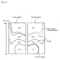
- the recombination lifetimes of the first and second samples are respectively shown in FIG.4 . As shown in FIG.4 , for the first sample, a region at which the recombination lifetime was the lowest was the region [Pi] and the highest region was the region [Pv]. For the second sample, a region at which the recombination lifetime was the lowest was the region [Pv] and the highest region was the region [Pi].
- the recombination lifetimes of the first and second samples are measured and the vertical measurement of the first sample is overlapped with the vertical measurement of the second sample (step (g1)).
- Cu was used as the first transition metal
- Ni was used as the second transition metal
- the recombination lifetimes of the first and second samples in which selective etching was carried out for the second sample were measured, and the vertical measurement of the first sample was overlapped with the vertical measurement of the second sample to obtain the result which is shown in FIG.6 .
- each of the horizontal axes corresponds to the axis direction of an ingot before the sample was cut.
- the region [Pv] and the region [Pi] can be identified from the kind of the transition metal and the dependency of the point defect region on the recombination lifetime.
- the identification of the region [Pv] and the region [Pi] can be realized by utilizing property that the recombination lifetimes at respective point defect regions are remarkably different depending on the kind of the transition metal, by staining with Ni and Cu the surface of each sample which is prepared from the same site of a crystal and measuring the distribution of the recombination lifetime after diffusion treatment.
- the first embodiment of the measurement method of the present invention is not an identification method in which oxygen dissolved in an ingot is a measurement objective, the method is not dependent on the concentration of oxygen dissolved in an ingot. Further, since the method is not influenced by the thermal heat treatment for oxygen precipitation condition, the method can identify the regions in high precision.
- the steps (a2) and (b2) are similar as the steps (a1) and (b1) of the first embodiment of the measurement method which are previously described.
- a first transition metal solution in which a first transition metal is dissolved at a concentration of 1 to 1000 ppm is coated on the surface of the first sample to stain the first sample with the metal (step (c2)).
- Cu is selected for the first transition metal hereat.
- a second transition metal solution in which a second transition metal different from the first transition metal is dissolved at a concentration of 1 to 1000 ppm is coated on the surface of the second sample to stain the second sample with the metal (step (d2)).
- Fe is selected for the second transition metal hereat.
- Diffusion thermal treatment is carried out for the first and second samples in the step (e2) at the similar condition as the step (e1) of the first embodiment of the measurement method previously described.
- the recombination lifetime of the transition metal is measured for the first and second samples (step (f2)).
- the LM-PCD is preferable for the measurement.
- the recombination lifetime is quantified over the whole sample by the LM-PCD.
- the recombination lifetimes of the first and second samples are respectively shown in FIGS.8 and 9 . As shown in FIG.8 , for the first sample, a region at which the recombination lifetime was highest was the region [Pi] and the lowest region was the region [V]. Further, as shown in FIG.9 , for the second sample, a region at which the recombination lifetime was lowest was the region [Pi] and the highest region was the region [Pv].
- the vertical measurement of the recombination lifetime of the first sample is overlapped with the vertical measurement of the second sample (step (g2)).
- the vertical concentration of the first transition metal is determined by the TID method for the first sample which is thermally treated (step (i2)).
- the concentration of the recombination center which is formed in a sample by Cu being the first transition metal is quantified by the TID method.
- the TID (Transient Ion Drift) method is a method by which the concentration of Cu dissolved in a silicon single crystal is quantified from the transient capacitance property of a metal semiconductor junction diode. It is assumed that Cu + ion (interstitial copper ion) is uniformly distributed at a space charge region in thermal equilibrium condition.
- the TID method is an evaluation method by which the quantification of the concentration change of the Cu + ion concentration accumulated in the space charge region from the zero bias condition can be realized by measuring the transient response attenuation property of junction capacitance.
- the vertical concentration of the second transition metal is determined by the DLTS method for the second sample thermally treated (step (j2)).
- the concentration of the recombination center which is formed in a sample by Fe being the second transition metal is quantified by the DLTS method.
- the DLTS (Deep Level Transient Spectroscopy) method is a method by which a pulse voltage to a positive direction is applied in a condition in which electric field to a reverse direction is applied to junction (or interface) and carrier is captured by the level of a depletion layer.
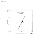
- the reciprocal number of the measurement value of the recombination lifetime of the first sample obtained in the step (f2) and the measurement value of the step (j2) are plotted to prepare a correlation straight line between the concentration of the first transition metal and the recombination lifetime (step (k2)).
- the correlation straight line prepared in the step (k2) is shown in FIG.11 .
- the reciprocal number of the measurement value of the recombination lifetime of the second sample obtained in the step (f2) and the measurement value of the step (j2) are plotted to prepare a correlation straight line between the concentration of the second transition metal and the recombination lifetime (step (12)).
- the correlation straight line prepared in the step (12) is shown in FIG.12 .
- the concentration of the recombination center at various point defect regions is determined from the correlation straight lines of FIGS.11 and 12 and it is grasped that the concentration of the recombination center differed remarkably depending on the kind of the transition metal and point defect species.
- each of the boundary between the regions [V] and [Pv] and the boundary between the regions [Pi] and [I] is specified from the correlation straight line of the step (k2) and the correlation straight line of the step (12) (step (m2)).
- the regions [Pv] and [Pi] can be identified by measuring the recombination lifetimes of the samples in which Cu and Fe are diffused, with the LM-PCD, by previously preparing correlation straight lines (calibration line).
- Each of the samples prepared from the same site of a crystal is stained with Cu and Fe on the surface thereof, the distribution of the recombination lifetime after diffusion thermal treatment is measured, and further, the correlation straight lines (calibration line) are prepared. Thereby, the identification of the regions [Pv] and [Pi] can be realized by utilizing the property that the recombination lifetimes at various point defect regions differ remarkably depending on the kind of the transition metal.
- the second embodiment of the measurement method of the present invention is not an identification method in which oxygen dissolved in an ingot is a measurement objective, the method is not dependent on the concentration of oxygen dissolved in an ingot. Further, since the method is not influenced by the thermal heat treatment for oxygen precipitation condition, the method can identify the regions in high precision.
- a sample for measurement is prepared from a test ingot (step (a3)). Namely, a p-type ingot is pulled up from silicon melt doped with boron which is stored in the quartz crucible of a pulling-up device based on the CZ method or MCZ method. At this time, the ingot is pulled up by changing the pulling-up speed V (mm/min.) of the ingot from a high speed (top side) to a low speed (bottom side), or a low speed (bottom side) to a high speed (top side) so that the above-mentioned regions [V], [Pv], [Pi] and [I] are contained to the axis direction of the ingot.
- V pulling-up speed
- sample for measurement having a thickness of 500 to 2000 ⁇ m whose surface is mirror-polished is prepared by cutting the ingot obtained in the test to axis direction and carrying out mirror-etching.
- the ingot is pulled up by changing the pulling-up speed V (mm/min.) from a high speed (top side) to a low speed (bottom side).
- a transition metal solution in which a transition metal M is dissolved at a concentration of 1 to 1000 ppm is coated on the sample to stain the sample with the metal (step (b3)).
- the transition metal M is preferably Fe.
- the transition metal solution is a solution in which the transition metal M is dissolved at a concentration of 1 to 1000 ppm and preferably 1 to 100 ppm.
- a standard solution for atomic absorption in which Fe is dissolved at a concentration of 10 to 100 ppm is preferred because of availability and superiority in concentration precision.
- the coating method includes the spin coat method, the dipping method and the like.
- the sample is rapidly heated at a temperature raising speed of 3.3°C/min. or more by rapidly charging the sample for measurement in a thermal treatment furnace which is retained at a first temperature of 600°C to 900°C under argon, nitrogen, oxygen, hydrogen or mixed gas atmosphere thereof, to thermally treat the sample for 0.5 hour to 4 hours, and the sample is rapidly cooled at a temperature lowering speed of 3.3°C/min. or more by rapidly taking the sample out from the thermal treatment furnace, to diffuse Fe which is coated on the surface into the whole sample (step (c3)).
- the rapid heating means that the sample is heated at a temperature raising speed of 3.3°C/min. or more, preferably 5°C/min. or more and further preferably 10°C/min.
- the rapid cooling means that the sample is cooled at a temperature lowering speed of 3.3°C/min. or more, preferably 5°C/min. or more and further preferably 10°C/min. or more.
- the thermal treatment method which is carried out does not carry out lumping treatment which is carried out in a conventional thermal treatment method and carries out the charging and taking-out of the sample in a thermal treatment furnace at a speed of 10 cm/min. to 150 cm/min. in order to rapidly heat the sample at a temperature raising speed of 3.3°C/min. or more and to rapidly cool the sample at a temperature lowering speed of 3.3°C/min.
- Fe diffused in the sample by carrying out the step (c3) Fe diffused forms a Fe-B bond which is a donor-acceptor pair with boron which exists at a lattice point position. Fe ion being cation is bound with B ion being anion by electrostatic attractive force and the bond forms a deep energy level of 0.1 eV in the energy band gap of silicon.
- concentration of the Fe-B bond of the sample to which diffusion thermal treatment is carried out depends on the concentration of oxygen dissolved in the crystal. This occurs because the formation density of precipitation nuclei differs in the respective regions of intrinsic point defects.
- the sample is rapidly heated at a temperature raising speed of 3.3°C/min. or more by rapidly charging the sample for measurement in a thermal treatment furnace which is retained at a second temperature of 450°C to 550°C, which is lower than the first temperature by 150°C to 450°C, under argon, nitrogen, oxygen, hydrogen or mixed gas atmosphere thereof, to thermally treat the sample for 0.5 hour to 4 hours, and the sample is rapidly cooled at a temperature lowering speed of 3.3°C/min. or more by rapidly taking the sample out from the thermal treatment furnace, to form metal silicide from Fe which is diffused into the whole sample (step (d3)).
- the charging and taking-out of the sample in the thermal treatment furnace in the step (d3) is carried out at a speed of 10 cm/min. to 150 cm/min. in like manner as the above-mentioned step (c3).
- the preparation rate of ⁇ -FeSi 2 at the regions [Pv] and [Pi] differs depending on the kind of intrinsic point defects at the respective regions.
- the step (d3) is carried out in order to make constant in a plane the concentration of Fe dissolved in the crystal, utilizing the dependency of ⁇ -FeSi 2 on the preparation rate and the kind of point defects at the respective regions.
- the thermal treatment is carried out at the second temperature of 500°C to 550°C for 0.5 to 1 hour.
- the second temperature and the retention time are less than the lower limit value, the metal silicide is not adequately formed. Further, when they exceed the upper limit value, a trouble that oxygen precipitate is formed in the crystal is generated.
- the sample is rapidly heated at a temperature raising speed of 3.3°C/min. or more by rapidly charging the sample in a thermal treatment furnace which is retained at a third temperature of 900°C to 1100°C, which is higher than the second temperature by 450°C to 550°C, under argon, nitrogen, oxygen, hydrogen or mixed gas atmosphere thereof, to thermally treat the sample for 0.5 hour to 4 hours, and the sample is rapidly cooled at a temperature lowering speed of 3.3°C/min. or more by rapidly taking the sample out from the thermal treatment furnace, to dissolve metal silicide which is formed in the inside of the sample (step (e3)).
- the charging and taking-out of the sample in the thermal treatment furnace in the step (e3) is carried out at a speed of 10 cm/min.
- the phase of ⁇ -FeSi 2 which is formed in the above-mentioned step (d3) is changed to ⁇ -FeSi 2 by carrying out the above-mentioned step (e3), to be electrically inactive. Further, the interstitial Fe which retained a Fe-B bond without forming ⁇ -FeSi 2 at the above-mentioned step (d3) is discharged. It is preferable in the dissolution thermal treatment that the thermal treatment is carried out at 900°C to 1000°C for 0.5 to 1 hour. When the third temperature and the retention time are less than the lower limit value, the metal silicide is not adequately formed. Further, when they exceed the upper limit value, a trouble that oxygen precipitate is formed in the crystal is generated.
- the concentration of recombination center which Fe forms in the whole sample to which the various thermal treatments of the above-mentioned steps (c3) to (e3) are carried out is measured by the DLTS, and a correlation function is determined based on the measurement value (step (f3)).
- the diffusion length of minor carrier of the sample is measured by the SPV method (surface photovoltage method) (step (g3)).
- SPV method surface photovoltage method
- step (g3) and the step (i3) described later only the interstitial Fe dissolved in the crystal and which is an electrically active defect is measured by the SPV method, utilizing the dependency of the re-discharge amount of Fe in the respective regions on the point defect species.
- Heat or optical energy is injected in the sample (step (h3)).
- a white light source of about 100 W is preferably irradiated to the sample.
- the Fe-B bond which exists in the sample become disjunct easily by irradiation of the white light source, and a deep energy level of 0.45 eV is formed in the energy band gap of the silicon single crystal.
- the diffusion length of minor carrier is decreased by the disjunction.
- the Fe ion being cation which become disjunct by injection of heat or optical energy is diffused in the inter-lattice of the crystal and forms again the Fe-B bond with most adjacent boron to carry out a reversible reaction.
- step (i3) the diffusion length of minor carrier of the sample to which heat or optical energy is injected is measured by the SPV method.
- the difference of the diffusion length of minor carrier is determined from the measurement value in the above-mentioned step (g3) before irradiation of the white light source and the measurement value in the above-mentioned step (i3) after irradiation (step (j3)).
- the difference obtained from the above-mentioned steps (g3) and (i3) is correlated with the concentration of Fe dissolved in the sample.
- the regions [Pi] and [Pv] and boundary thereof are specified from the correlation function obtained in the above-mentioned step (f3) and the diffusion length of minor carrier obtained in the above-mentioned step (j3) (step (k3)). Since the re-discharge amount of Fe depends remarkably on the kind of the point defect regions, the regions [Pi] and [Pv] and boundary thereof can be specified by determining the product of the correlation function with the difference of the diffusion length of minor carrier.
- the quantification of the in-plane concentration of Fe is realized by respectively measuring the diffusion lengths at an assigned position of the wafer using the measurement value of the diffusion length of minor carrier before and after irradiation of the white light source, by assembling the correlation function preliminarily obtained from the DLTS, in the measurement soft of an SPV measurement device.
- the transition metal (Fe) which is trapped with boron being a gettering sink and formed a Fe-B bond is interstitially discharged again by dissolution thermal treatment at the region [Pi] in which the concentration of vacancy is a low concentration.
- Fe which formed a Fe-B bond is introduced in a vacancy by dissolution thermal treatment at the region [Pv] in which the concentration of vacancy is high, and precipitation is accelerated.
- the concentration of the transition metal in the region [Pi] is a concentration of about 3-fold or more in comparison with the concentration of the transition metal in the region [Pv].
- not claimed measurement method is not an identification method in which oxygen dissolved in the ingot is an objective for measurement, the method is not dependent on the concentration of oxygen dissolved in the ingot and the thermal heat treatment for oxygen precipitation for a long time is also unnecessary. Since the method is not influenced by the thermal heat treatment for oxygen precipitation condition, the method can identify the regions in high precision.
- an ingot was pulled up by changing a pulling-up speed from silicon melt doped with boron so as to respectively include regions [V], [Pv], [Pi] and [I], and the ingot was sliced to diameter direction at a position including the regions [Pv] and [Pi] which are situated at the A-A line of FIG.23 , to obtain 8 samples.
- a solution with 100 ppm of Fe was coated on the surface of the 8 samples to stain the surface of the samples with the metal.
- thermal treatment was carried out to each of the 8 samples at conditions shown in Table 1 below.
- the concentrations of recombination center which Fe formed in the whole sample were measured by the DLTS method with respect to the samples which terminated the thermal treatment at various conditions and correlation functions were determined based on the measurement values.
- the diffusion lengths of minor carrier were measured using the SPV method.
- a white light source was irradiated on each of the samples.
- the diffusion lengths of minor carrier after irradiation of the white light source were measured using the SPV method.
- the differences of the diffusion lengths of minor carrier before and after irradiation of the white light source were determined.
- the diffusion lengths (in-plane distribution) of the concentration of the recombination center of Fe in the samples were measured from the correlation functions and the differences of the diffusion lengths of minor carrier.
- the distribution to diameter direction of the concentration of recombination center of Fe which were obtained form various point defect regions in the Fe diffused samples is shown in FIG.15 . Further, the distribution chart of the concentration of the recombination centers of Fe at 0 mm to 50 mm from the wafer center of FIG.15 is shown in FIG.16 . Furthermore, the distribution charts of the in-plane wafer of the concentration of Fe at the regions [Pv] and [Pi] in Control Examples 2 and 3 and Comparative Examples 1, 2, 4 and 5 are shown in FIGS.17 to 22 .
- the concentration Fe differs remarkably in the respective regions depending on the temperature condition of the thermal treatment. It was the region [Pi] of Control Example 2 that the concentration of Fe was highest and it was the region [Pv] of Comparative Example 4 that the concentration of Fe was lowest. Thus, it is grasped that the concentration of Fe detected differs depending on the condition of thermal treatment and the respective regions. The result shows that the identification and judgment of the respective regions can be carried out using the dependency of the concentration of Fe on the temperature of dissolution thermal treatment.
- FIGS.17 to 22 are the in-plane distribution of the wafer of the concentration of Fe at the regions [Pv] and [Pi] in Control Examples 2 and 3 and Comparative Examples 1, 2, 4 and 5. Since Fe is not adequately recombined in Comparative Example 1 in which only diffusion thermal treatment was carried out and Comparative Example 2 in which melting thermal treatment was not carried out, an adequate in-plane distribution was not obtained and the respective regions cannot be identified. In Comparative Examples 4 and 5 in which the dissolution thermal treatment at less than 900°C was carried out, an adequate recombination distribution was not obtained and the respective regions cannot be identified.
- the method for measuring the point defect distribution of a silicon single crystal ingot of the present invention can identify the regions [Pv] and [Pi] in the ingot and boundary thereof with high precision and in a short time. Since the regions [Pv] and [Pi] can be clearly judged by the present invention, V/G control which has been a problem when a defect-free silicon single crystal is conventionally produced can be precisely controlled and the stable mass production of a defect-free silicon single crystal can be realized.
Landscapes
- Chemical & Material Sciences (AREA)
- Engineering & Computer Science (AREA)
- Materials Engineering (AREA)
- Organic Chemistry (AREA)
- Crystallography & Structural Chemistry (AREA)
- Ceramic Engineering (AREA)
- Metallurgy (AREA)
- Structural Engineering (AREA)
- Chemical Kinetics & Catalysis (AREA)
- Inorganic Chemistry (AREA)
- Crystals, And After-Treatments Of Crystals (AREA)
- Testing Or Measuring Of Semiconductors Or The Like (AREA)
Claims (7)
- Verfahren zur Messung der Punktdefekt-Verteilung eines Silicium-Einkristall-Ingots, umfassend
(a1) einen Schritt, bei dem eine Probe zur Messung, die die Regionen [V], [Pv], [Pi] und [I] einschließt, hergestellt wird, indem ein Silicium-Einkristall-Ingot, der durch Ändern einer Herausziehgeschwindigkeit aus einer Siliciumschmelze herausgezogen wird, in axialer Richtung derart geschnitten wird, dass er die zentrale Achse des Einkristall-Ingots einschließt,
(b 1) einen Schritt, bei dem eine erste Probe und eine zweite Probe hergestellt werden, indem die Probe zur Messung in zwei derart geteilt wird, dass sie symmetrisch gegen die zentrale Achse des Ingots ist,
(c1) einen Schritt, bei dem die Oberfläche der ersten Probe mit einer ersten Übergangsmetalllösung beschichtet wird, in der ein erstes Übergangsmetall in einer Konzentration von 1 bis 1000 ppm gelöst ist, um die Probe mit dem Metall zu färben,
(d1)einen Schritt, bei dem die Oberfläche der zweiten Probe mit einer zweiten Übergangsmetalllösung beschichtet wird, in der ein zweites, zum ersten Übergangsmetall verschiedenes Übergangsmetall in einer Konzentration von 1 bis 1000 ppm gelöst ist, um die Probe mit dem Metall zu färben,
(e1) einen thermischen Diffusionsbehandlungsschritt, bei dem die erste und zweite Probe, die mit den Metallen gefärbt sind, 0,5 Stunden bis 30 Stunden bei 600 °C bis 1150 °C unter einer Argon-, Stickstoff-, Sauerstoff-, Wasserstoff- oder Mischgasatmosphäre davon thermisch behandelt werden und das erste und zweite Übergangsmetall, mit denen die Oberfläche der ersten bzw. zweiten Probe beschichtet ist, in das Innere der Proben diffundieren,
(f1) einen Schritt, bei dem jeweils Rekombinations-Lebensdauem im Gesamten der ersten und zweiten Probe, die thermisch behandelt sind, gemessen werden,
(g1) einen Schritt, bei dem die vertikale Messung der ersten Probe von Schritt (f1) der vertikalen Messung der zweiten Probe überlagert wird, und
(h1)einen Schritt, bei dem jeweils die Grenze zwischen den Regionen [Pi] und [I] und die Grenze zwischen den Regionen [V] und [Pv] aus dem Messergebnis von Schritt (g1) spezifiziert wird;
mit der Maßgabe, dass die Region [V] eine Region mit Defekten ist, wobei der Punktdefekt vom Leerstellen-Typ dominant ist und übermäßige Leerstellen agglomeriert sind, die Region [Pv] eine Region mit Defekten ist, wobei der Punktdefekt vom Leerstellen-Typ dominant ist und Leerstellen nicht agglomeriert sind, die Region [Pi] eine Region mit Defekten ist, wobei der Punktdefekt vom Zwischengitter-Silicium-Typ dominant ist und Zwischengitter-Silicium nicht agglomeriert ist, und die Region [I] eine Region mit Defekten ist, wobei der Punktdefekt vom Zwischengitter-Silicium-Typ dominant ist und Zwischengitter-Silicium nicht agglomeriert ist. - Messverfahren nach Anspruch 1, wobei das Verfahren nach dem Schritt (g1) weiterhin umfasst,
(i1) einen Schritt, bei dem die vertikale Konzentration des ersten Übergangsmetalls durch die TID-Methode bezüglich der ersten Probe, die thermisch behandelt ist, bestimmt wird,
(j1) einen Schritt, bei dem die vertikale Konzentration des zweiten Übergangsmetalls durch die DLTS-Methode bezüglich der zweiten Probe, die thermisch behandelt ist, bestimmt wird,
(k1) einen Schritt, bei dem eine gerade Korrelationslinie zwischen der Konzentration des ersten Übergangsmetalls und der Rekombinations-Lebensdauer aus dem Ergebnis der vertikalen Messung in der ersten Probe von Schritt (f1) und dem Messergebnis von Schritt (i1) erstellt wird, (11) einen Schritt, bei dem eine gerade Korrelationslinie zwischen der Konzentration des zweiten Übergangsmetalls und der Rekombinations-Lebensdauer aus dem Ergebnis der vertikalen Messung in der zweiten Probe von Schritt (f1) und dem Messergebnis von Schritt (j1) erstellt wird, und
(m1)einen Schritt, bei dem jeweils die Grenze zwischen den Regionen [V] und [Pv] und die Grenze zwischen den Regionen [Pi] und [I] aus dem Messergebnis von Schritt (g1), der geraden Korrelationslinie von Schritt (k1) und der geraden Korrelationslinie von (11) spezifiziert wird,
mit der Maßgabe, dass die TID-Methode eine Methode zur Quantifizierung der Konzentration an in einem Silicium-Einkristall gelösten Cu aus der Analyse einer Übergangs-Kapazitanz-Eigenschaft einer Metallhalbleiter-Flächendiode ist und die DLTS-Methode eine Methode zum Anlegen einer Pulsspannung in positiver Richtung in einem Zustand ist, in dem ein elektrisches Feld in umgekehrter Richtung gegen die Verbindung (oder Schnittstelle) ist, und zum Fangen eines Trägers bei einem Level in einer Verarmungszone. - Messverfahren nach Anspruch 1, wobei das erste Übergangsmetall Cu oder Fe ist und das zweite Übergangsmetall Ni oder Co ist.
- Messverfahren nach Anspruch 2, wobei das erste Übergangsmetall Cu ist und das zweite Übergangsmetall Fe ist.
- Messverfahren nach Anspruch 1 oder 2, wobei es sich bei dem thermischen Diffusionsbehandlungsschritt des ersten und zweiten Übergangsmetalls in Schritt (e1) um eine thermische Behandlung bei 600 °C bis 1150 °C für 0,5 Stunden bis 24 Stunden handelt.
- Messverfahren nach Anspruch 1 oder 2, wobei die Messung der Rekombinations-Lebensdauer in Schritt (f1) unter Verwendung von LM-PCD (Laser/Mikrowellen-Fotokonduktanz-Zerfallsmethode) erfolgt.
- Messverfahren nach Anspruch 1 oder 3, weiterhin umfassend einen Schritt des selektiven Ätzens der Oberfläche der zweiten Probe, die thermisch in Schritt (e1) behandelt wird, wenn das zweite Übergangsmetall, mit dem die zweite Probe Metall-gefärbt ist, Ni ist.
Priority Applications (1)
| Application Number | Priority Date | Filing Date | Title |
|---|---|---|---|
| EP09001440A EP2077346B1 (de) | 2002-10-18 | 2003-10-17 | Verfahren zur Bestimmung der Punktdefektverteilung eines Siliciumeinkristallstabs |
Applications Claiming Priority (3)
| Application Number | Priority Date | Filing Date | Title |
|---|---|---|---|
| JP2002304410 | 2002-10-18 | ||
| JP2002304410 | 2002-10-18 | ||
| PCT/JP2003/013320 WO2004035879A1 (ja) | 2002-10-18 | 2003-10-17 | シリコン単結晶インゴットの点欠陥分布を測定する方法 |
Related Child Applications (2)
| Application Number | Title | Priority Date | Filing Date |
|---|---|---|---|
| EP09001440A Division EP2077346B1 (de) | 2002-10-18 | 2003-10-17 | Verfahren zur Bestimmung der Punktdefektverteilung eines Siliciumeinkristallstabs |
| EP09001440.8 Division-Into | 2009-02-03 |
Publications (3)
| Publication Number | Publication Date |
|---|---|
| EP1559812A1 EP1559812A1 (de) | 2005-08-03 |
| EP1559812A4 EP1559812A4 (de) | 2008-06-25 |
| EP1559812B1 true EP1559812B1 (de) | 2010-12-15 |
Family
ID=32105109
Family Applications (2)
| Application Number | Title | Priority Date | Filing Date |
|---|---|---|---|
| EP09001440A Expired - Lifetime EP2077346B1 (de) | 2002-10-18 | 2003-10-17 | Verfahren zur Bestimmung der Punktdefektverteilung eines Siliciumeinkristallstabs |
| EP03756681A Expired - Lifetime EP1559812B1 (de) | 2002-10-18 | 2003-10-17 | Verfahren zur bestimmung derpunktdefektverteilung eines siliciumeinkristallstabs |
Family Applications Before (1)
| Application Number | Title | Priority Date | Filing Date |
|---|---|---|---|
| EP09001440A Expired - Lifetime EP2077346B1 (de) | 2002-10-18 | 2003-10-17 | Verfahren zur Bestimmung der Punktdefektverteilung eines Siliciumeinkristallstabs |
Country Status (7)
| Country | Link |
|---|---|
| US (1) | US7244306B2 (de) |
| EP (2) | EP2077346B1 (de) |
| KR (1) | KR100722089B1 (de) |
| AU (1) | AU2003301326A1 (de) |
| DE (2) | DE60335409D1 (de) |
| TW (1) | TWI231357B (de) |
| WO (1) | WO2004035879A1 (de) |
Families Citing this family (17)
| Publication number | Priority date | Publication date | Assignee | Title |
|---|---|---|---|---|
| JPWO2005073439A1 (ja) * | 2004-02-02 | 2007-09-13 | 信越半導体株式会社 | シリコン単結晶及びシリコンウェーハ及びそれらの製造装置並びに製造方法 |
| JP4743010B2 (ja) * | 2005-08-26 | 2011-08-10 | 株式会社Sumco | シリコンウェーハの表面欠陥評価方法 |
| US7901132B2 (en) * | 2006-09-25 | 2011-03-08 | Siltron Inc. | Method of identifying crystal defect region in monocrystalline silicon using metal contamination and heat treatment |
| KR100818670B1 (ko) * | 2006-09-25 | 2008-04-01 | 주식회사 실트론 | 금속 오염과 열처리를 이용한 단결정 실리콘의 결정 결함영역 구분 방법 |
| US8008107B2 (en) * | 2006-12-30 | 2011-08-30 | Calisolar, Inc. | Semiconductor wafer pre-process annealing and gettering method and system for solar cell formation |
| JP5659632B2 (ja) * | 2010-08-27 | 2015-01-28 | 株式会社Sumco | ボロンドープp型シリコンウェーハの鉄濃度分析方法および分析装置、シリコンウェーハ、ならびにシリコンウェーハの製造方法 |
| KR101242353B1 (ko) * | 2011-06-28 | 2013-03-15 | 주식회사 엘지실트론 | 실리콘 웨이퍼의 결함 평가 방법 |
| KR101339624B1 (ko) * | 2012-09-07 | 2013-12-09 | 주식회사 엘지실트론 | 단결정 실리콘 웨이퍼 및 반도체 웨이퍼 |
| WO2014109453A1 (en) | 2013-01-08 | 2014-07-17 | Lg Siltron Inc. | Silicon single crystal wafer, manufacturing method thereof and method of detecting defects |
| KR101525657B1 (ko) * | 2013-01-08 | 2015-06-03 | 주식회사 엘지실트론 | 실리콘 단결정 웨이퍼 및 그 제조 방법 |
| JP6036670B2 (ja) * | 2013-12-10 | 2016-11-30 | 信越半導体株式会社 | シリコン単結晶基板の欠陥濃度評価方法 |
| JP7057122B2 (ja) | 2017-12-22 | 2022-04-19 | グローバルウェーハズ・ジャパン株式会社 | 金属汚染評価方法 |
| JP6852703B2 (ja) * | 2018-03-16 | 2021-03-31 | 信越半導体株式会社 | 炭素濃度評価方法 |
| JP7345379B2 (ja) * | 2019-12-06 | 2023-09-15 | 株式会社ディスコ | ゲッタリング性評価装置 |
| JP7694145B2 (ja) * | 2021-05-21 | 2025-06-18 | 株式会社Sumco | シリコン単結晶インゴットの評価方法、シリコンエピタキシャルウェーハの評価方法、シリコンエピタキシャルウェーハの製造方法およびシリコン鏡面ウェーハの評価方法 |
| CN113782465B (zh) * | 2021-11-11 | 2022-02-18 | 西安奕斯伟材料科技有限公司 | 用于检测晶圆表面金属的方法 |
| CN115763293A (zh) * | 2022-11-30 | 2023-03-07 | 西安奕斯伟材料科技有限公司 | 用于监测半导体制程体金属的方法 |
Family Cites Families (13)
| Publication number | Priority date | Publication date | Assignee | Title |
|---|---|---|---|---|
| US5418172A (en) * | 1993-06-29 | 1995-05-23 | Memc Electronic Materials S.P.A. | Method for detecting sources of contamination in silicon using a contamination monitor wafer |
| US6045610A (en) * | 1997-02-13 | 2000-04-04 | Samsung Electronics Co., Ltd. | Methods of manufacturing monocrystalline silicon ingots and wafers by controlling pull rate profiles in a hot zone furnance |
| KR19980070037A (ko) * | 1997-02-13 | 1998-10-26 | 윤종용 | 반도체 잉곳 성장시 시드결정의 인상속도 최적화방법, 이를 적용한 반도체 잉곳 성장방법, 그에 따라 성장된 반도체 잉곳과반도체 웨이퍼 및 반도체장치 |
| SG64470A1 (en) | 1997-02-13 | 1999-04-27 | Samsung Electronics Co Ltd | Methods of manufacturing monocrystalline silicon ingots and wafers by controlling pull rate profiles in a hot zone furnace and ingots and wafers manufactured thereby |
| US6379642B1 (en) * | 1997-04-09 | 2002-04-30 | Memc Electronic Materials, Inc. | Vacancy dominated, defect-free silicon |
| MY135749A (en) * | 1997-04-09 | 2008-06-30 | Memc Electronic Materials | Process for producing low defect density, ideal oxygen precipitating silicon |
| EP1273684B1 (de) * | 1997-04-09 | 2005-09-14 | MEMC Electronic Materials, Inc. | Freistellenbeherrschendes Silizium mit niedriger Fehlerdichte |
| KR100252214B1 (ko) * | 1997-04-23 | 2000-04-15 | 윤종용 | 반도체장치 제조용 베어 웨이퍼 분석방법 |
| JP2001102385A (ja) | 1999-07-28 | 2001-04-13 | Mitsubishi Materials Silicon Corp | 点欠陥の凝集体が存在しないシリコンウェーハ |
| SE0000095L (sv) * | 2000-01-14 | 2001-07-15 | Electrolux Ab | Spjäll för reglering av tillsatsluft till tvåtakts förbränningsmotorer |
| IES20010113A2 (en) * | 2000-02-11 | 2001-09-19 | Anthony Herbert | An atmospheric pressure plasma system |
| JP3890861B2 (ja) * | 2000-07-31 | 2007-03-07 | 株式会社Sumco | シリコン単結晶の引上げ方法 |
| US7074271B2 (en) * | 2004-02-23 | 2006-07-11 | Sumitomo Mitsubishi Silicon Corporation | Method of identifying defect distribution in silicon single crystal ingot |
-
2003
- 2003-10-17 EP EP09001440A patent/EP2077346B1/de not_active Expired - Lifetime
- 2003-10-17 EP EP03756681A patent/EP1559812B1/de not_active Expired - Lifetime
- 2003-10-17 DE DE60335409T patent/DE60335409D1/de not_active Expired - Lifetime
- 2003-10-17 WO PCT/JP2003/013320 patent/WO2004035879A1/ja not_active Ceased
- 2003-10-17 DE DE03756681T patent/DE03756681T1/de active Pending
- 2003-10-17 TW TW092128828A patent/TWI231357B/zh not_active IP Right Cessation
- 2003-10-17 KR KR1020057006712A patent/KR100722089B1/ko not_active Expired - Lifetime
- 2003-10-17 US US10/531,434 patent/US7244306B2/en not_active Expired - Lifetime
- 2003-10-17 AU AU2003301326A patent/AU2003301326A1/en not_active Abandoned
Also Published As
| Publication number | Publication date |
|---|---|
| US7244306B2 (en) | 2007-07-17 |
| EP2077346A2 (de) | 2009-07-08 |
| DE60335409D1 (de) | 2011-01-27 |
| KR20050067417A (ko) | 2005-07-01 |
| DE03756681T1 (de) | 2005-12-29 |
| EP2077346A3 (de) | 2010-02-24 |
| EP1559812A1 (de) | 2005-08-03 |
| US20060130738A1 (en) | 2006-06-22 |
| EP2077346B1 (de) | 2012-09-26 |
| KR100722089B1 (ko) | 2007-05-25 |
| EP1559812A4 (de) | 2008-06-25 |
| WO2004035879A1 (ja) | 2004-04-29 |
| TWI231357B (en) | 2005-04-21 |
| TW200412421A (en) | 2004-07-16 |
| AU2003301326A1 (en) | 2004-05-04 |
Similar Documents
| Publication | Publication Date | Title |
|---|---|---|
| EP1559812B1 (de) | Verfahren zur bestimmung derpunktdefektverteilung eines siliciumeinkristallstabs | |
| KR100768378B1 (ko) | 실리콘 웨이퍼 및 실리콘 웨이퍼 표면 결함 평가 방법 | |
| Yamagishi et al. | Recognition of D defects in silicon single crystals by preferential etching and effect on gate oxide integrity | |
| US7732352B2 (en) | Silicon wafers and method of fabricating the same | |
| KR100369760B1 (ko) | 실리콘 웨이퍼의 제조 방법 | |
| TWI539041B (zh) | 單晶矽半導體晶圓及其製造方法 | |
| US6641888B2 (en) | Silicon single crystal, silicon wafer, and epitaxial wafer. | |
| EP0948037A1 (de) | Epitaxialscheibe aus silizium und verfahren zu deren herstellung | |
| JPH08298233A (ja) | 正確に定められた深さの無欠陥層を有する較正用ウエーハの製造方法および較正用ウエーハ | |
| WO2013112779A1 (en) | Qualitative crystal defect evaluation method | |
| US20020142170A1 (en) | Silicon single crystal, silicon wafer, and epitaxial wafer | |
| US7074271B2 (en) | Method of identifying defect distribution in silicon single crystal ingot | |
| JP3933010B2 (ja) | シリコン単結晶インゴットの点欠陥分布を測定する方法 | |
| TWI694183B (zh) | 由單晶矽製成的半導體晶圓 | |
| JP4200845B2 (ja) | シリコン単結晶インゴットの点欠陥分布を測定する方法 | |
| JP3915606B2 (ja) | シリコン単結晶インゴットの点欠陥分布を測定する方法 | |
| Papakonstantinou et al. | Crystal surface defects and oxygen gettering in thermally oxidized bonded SOI wafers | |
| EP1127962B1 (de) | Verfahren zur herstellung eines siliziumeinkristalls damit hergestellter siliziumeinkristall und siliziumwafer | |
| JP4124151B2 (ja) | Igウェーハの製造方法 |
Legal Events
| Date | Code | Title | Description |
|---|---|---|---|
| PUAI | Public reference made under article 153(3) epc to a published international application that has entered the european phase |
Free format text: ORIGINAL CODE: 0009012 |
|
| 17P | Request for examination filed |
Effective date: 20050511 |
|
| AK | Designated contracting states |
Kind code of ref document: A1 Designated state(s): AT BE BG CH CY CZ DE DK EE ES FI FR GB GR HU IE IT LI LU MC NL PT RO SE SI SK TR |
|
| AX | Request for extension of the european patent |
Extension state: AL LT LV MK |
|
| EL | Fr: translation of claims filed | ||
| DET | De: translation of patent claims | ||
| DAX | Request for extension of the european patent (deleted) | ||
| RBV | Designated contracting states (corrected) |
Designated state(s): DE FR IT |
|
| RAP1 | Party data changed (applicant data changed or rights of an application transferred) |
Owner name: SUMCO CORPORATION |
|
| A4 | Supplementary search report drawn up and despatched |
Effective date: 20080526 |
|
| 17Q | First examination report despatched |
Effective date: 20080821 |
|
| RIN1 | Information on inventor provided before grant (corrected) |
Inventor name: KURITA, KAZUNARIC/O SUMCO COPRORATION Inventor name: FURUKAWA, JUNC/O SUMCO CORPORATION |
|
| RIN1 | Information on inventor provided before grant (corrected) |
Inventor name: KURITA, KAZUNARIC/O SUMCO COPRORATION |
|
| GRAP | Despatch of communication of intention to grant a patent |
Free format text: ORIGINAL CODE: EPIDOSNIGR1 |
|
| GRAS | Grant fee paid |
Free format text: ORIGINAL CODE: EPIDOSNIGR3 |
|
| GRAA | (expected) grant |
Free format text: ORIGINAL CODE: 0009210 |
|
| AK | Designated contracting states |
Kind code of ref document: B1 Designated state(s): DE FR IT |
|
| REF | Corresponds to: |
Ref document number: 60335409 Country of ref document: DE Date of ref document: 20110127 Kind code of ref document: P |
|
| PLBE | No opposition filed within time limit |
Free format text: ORIGINAL CODE: 0009261 |
|
| STAA | Information on the status of an ep patent application or granted ep patent |
Free format text: STATUS: NO OPPOSITION FILED WITHIN TIME LIMIT |
|
| 26N | No opposition filed |
Effective date: 20110916 |
|
| REG | Reference to a national code |
Ref country code: DE Ref legal event code: R097 Ref document number: 60335409 Country of ref document: DE Effective date: 20110916 |
|
| REG | Reference to a national code |
Ref country code: FR Ref legal event code: PLFP Year of fee payment: 13 |
|
| REG | Reference to a national code |
Ref country code: FR Ref legal event code: PLFP Year of fee payment: 14 |
|
| REG | Reference to a national code |
Ref country code: FR Ref legal event code: PLFP Year of fee payment: 15 |
|
| REG | Reference to a national code |
Ref country code: FR Ref legal event code: PLFP Year of fee payment: 16 |
|
| PGFP | Annual fee paid to national office [announced via postgrant information from national office to epo] |
Ref country code: FR Payment date: 20221028 Year of fee payment: 20 |
|
| PGFP | Annual fee paid to national office [announced via postgrant information from national office to epo] |
Ref country code: IT Payment date: 20221026 Year of fee payment: 20 Ref country code: DE Payment date: 20221019 Year of fee payment: 20 |
|
| REG | Reference to a national code |
Ref country code: DE Ref legal event code: R071 Ref document number: 60335409 Country of ref document: DE |