EP1557876A1 - Sondenmarkierungsleser und sondenmarkierungsleseverfahren - Google Patents
Sondenmarkierungsleser und sondenmarkierungsleseverfahren Download PDFInfo
- Publication number
- EP1557876A1 EP1557876A1 EP03754153A EP03754153A EP1557876A1 EP 1557876 A1 EP1557876 A1 EP 1557876A1 EP 03754153 A EP03754153 A EP 03754153A EP 03754153 A EP03754153 A EP 03754153A EP 1557876 A1 EP1557876 A1 EP 1557876A1
- Authority
- EP
- European Patent Office
- Prior art keywords
- probe mark
- electrode
- photographing
- probe
- electrodes
- Prior art date
- Legal status (The legal status is an assumption and is not a legal conclusion. Google has not performed a legal analysis and makes no representation as to the accuracy of the status listed.)
- Withdrawn
Links
Images


Classifications
-
- G—PHYSICS
- G06—COMPUTING OR CALCULATING; COUNTING
- G06T—IMAGE DATA PROCESSING OR GENERATION, IN GENERAL
- G06T7/00—Image analysis
- G06T7/0002—Inspection of images, e.g. flaw detection
- G06T7/0004—Industrial image inspection
-
- H—ELECTRICITY
- H10—SEMICONDUCTOR DEVICES; ELECTRIC SOLID-STATE DEVICES NOT OTHERWISE PROVIDED FOR
- H10P—GENERIC PROCESSES OR APPARATUS FOR THE MANUFACTURE OR TREATMENT OF DEVICES COVERED BY CLASS H10
- H10P74/00—Testing or measuring during manufacture or treatment of wafers, substrates or devices
-
- G—PHYSICS
- G01—MEASURING; TESTING
- G01R—MEASURING ELECTRIC VARIABLES; MEASURING MAGNETIC VARIABLES
- G01R31/00—Arrangements for testing electric properties; Arrangements for locating electric faults; Arrangements for electrical testing characterised by what is being tested not provided for elsewhere
- G01R31/28—Testing of electronic circuits, e.g. by signal tracer
- G01R31/2851—Testing of integrated circuits [IC]
- G01R31/2886—Features relating to contacting the IC under test, e.g. probe heads; chucks
- G01R31/2891—Features relating to contacting the IC under test, e.g. probe heads; chucks related to sensing or controlling of force, position, temperature
-
- G—PHYSICS
- G01—MEASURING; TESTING
- G01R—MEASURING ELECTRIC VARIABLES; MEASURING MAGNETIC VARIABLES
- G01R31/00—Arrangements for testing electric properties; Arrangements for locating electric faults; Arrangements for electrical testing characterised by what is being tested not provided for elsewhere
- G01R31/28—Testing of electronic circuits, e.g. by signal tracer
- G01R31/302—Contactless testing
- G01R31/308—Contactless testing using non-ionising electromagnetic radiation, e.g. optical radiation
- G01R31/311—Contactless testing using non-ionising electromagnetic radiation, e.g. optical radiation of integrated circuits
-
- G—PHYSICS
- G06—COMPUTING OR CALCULATING; COUNTING
- G06T—IMAGE DATA PROCESSING OR GENERATION, IN GENERAL
- G06T2207/00—Indexing scheme for image analysis or image enhancement
- G06T2207/30—Subject of image; Context of image processing
- G06T2207/30108—Industrial image inspection
- G06T2207/30148—Semiconductor; IC; Wafer
Definitions
- the present invention relates to a probe mark reading device and a probe mark reading method for reading probe marks formed on electrodes by examining electrical characteristics of a prescribed object.
- test probes are pressed against electrodes within the semiconductor chip. Electrodes are typically made from aluminum and are typically covered in an insulating aluminum oxide covering formed by oxidation at the time of examination. The test probe is therefore pushed against the electrode with a certain amount of force in order to break through the covering. As a result, probe marks (contact imprints) are formed by the test probe. A determination can then be made as to whether or not the test probe has been correctly pushed against the electrode by reading probe mark conditions such as the presence or absence, position, and depth etc. of a probe mark.
- probe mark reading devices for reading conditions for probe marks.
- a probe mark reading device is disclosed where a semiconductor wafer on which semiconductor chips are formed is mounted on a stage. Images obtained by taking pictures of probe marks formed on electrodes with a CCD camera are then stored and displayed in an appropriate manner. With this configuration, age deterioration in a probe mark is checked and temporal changes in test probe pin-pressure and pin-shifts can be managed.
- detecting targets different from the electrodes such as, for example, tape inspecting devices for inspecting repetitive patterns disclosed in Japanese Patent Laid-open Publication No. Hei. 9-222311 (and the corresponding US Patent No. 5, 808, 744), mark position detection devices for detecting alignment marks on a wafer as disclosed in, for example, Japanese Patent Laid-open Publication No. Hei. 10-281729, or sample surface scanning devices for examining for foreign bodies or blemishes on a wafer surface disclosed in, for example, Japanese Patent Laid-open Publication No. Hei. 10-281729, a target is sequentially photographed by moving the target and emitting a flash of light at the position of the target in a synchronized manner.
- devices for detecting a target different from an electrode, that move the target in the manner described above while taking a series of photographs also exist (for example, refer to Japanese Laid-open Publication No. Hei. 9-222311, Japanese Laid-open Patent Publication No. 10-281729, and Japanese Patent Publication No. Hei. 11-326233).
- photographing can take place in a short period of time without being troublesome to the user.
- photographing is repeated at the same period and a photographing is carried out at a high-speed by making the picture-taking interval fixed.
- the arrangement is unlikely to be at equal intervals, and it is not planned to take pictures at high speed of a target for which arrangement position may be changed (depending on the wafer).
- the above devices therefore cannot be easily used as devices for reading a multiplicity of probe marks formed at a multiplicity of electrodes.
- an object of the present invention to provide a probe mark reading device and probe mark reading method for reading a probe mark without posing a great deal of trouble to a user and in a short period of time.
- a probe mark reading device for reading, when testing electrical characteristics of a target object having a plurality of electrodes, probe marks formed on the electrodes.
- This device comprises: an illuminating mechanism which illuminates an electrode as a photographing target among the plurality of electrodes; a photographing mechanism which photographs at least part of at least one electrode illuminated by the illuminating mechanism at a photographing position thereof to obtain image information of the electrode, the photographing mechanism being supplied with an image of at least one electrode for a predetermined period of time at the photographing position; a photographing target position changing mechanism to sequentially place at least one electrode as a photographing target among the plurality of electrodes at the photographing position of the photographing mechanism; and a memory which stores the image information obtained by the photographing mechanism.
- a probe mark reading device for reading, when testing electrical characteristics of a target object having a plurality of electrodes, probe marks formed on the electrodes.
- This probe mark reading device comprises: an illuminating mechanism which illuminates an electrode as a photographing target among the plurality of electrodes; a photographing mechanism which photographs at least part of at least one electrode illuminated by the illuminating mechanism at a photographing position thereof to obtain image information of the electrode, the photographing mechanism being supplied with an image of at least one electrode for a predetermined period of time at the photographing position; a photographing target position changing mechanism to sequentially place at least one electrode as a photographing target among the plurality of electrodes at the photographing position of the photographing mechanism; and a memory which stores the image information obtained by the photographing mechanism.
- the probe mark reading device preferably includes at least one of the following (a) to (h) or some of them.
- a probe mark test device for testing, when testing electrical characteristics of a target object having a plurality of electrodes, probe marks formed on the electrodes.
- the probe mark test device comprises: an initial vector calculating mechanism which calculates an initial vector from a position of a pre-registered model probe mark to a position of a probe mark formed on a predetermined electrode among the plurality of electrodes; and a probe mark non-defectiveness/defectiveness determination mechanism which determines whether or not a probe mark formed on the electrode photographed by the photographing mechanism is located within a predetermined determination range including a position in a direction and distance of the initial vector from the position of the pre-registered model probe mark relating to an electrode different from the predetermined electrode.
- a probe mark reading method for reading, when testing electrical characteristics of a target object including a plurality of electrodes, probe marks formed on the electrodes.
- the probe mark reading method comprises: (a1) placing an electrode at a photographing position of a photographing mechanism (20); (a2) illuminating by an illuminating mechanism the electrode placed at the photographing position; (a3) photographing the illuminated electrode with the photographing mechanism and outputting image information obtained by photographing, the photographing mechanism being supplied with an image of the electrode during a predetermined period of time while the electrode is to be photographed; and (a4) receiving and storing the image information.
- the invention provided according to the third aspect of the present invention preferably comprises at least one of the following (i) to (l), or a combination of some of them.
- a probe mark test method of testing when testing electrical characteristics of a target object including a plurality of electrodes, probe marks formed on the electrodes.
- the probe mark testing method comprises: (b1) calculating an initial vector as a vector from a position of a pre-registered model probe mark to a position of a probe mark formed on a predetermined electrode among the plurality of electrodes; and (b2) determining non-defectiveness/defectiveness of the probe mark, determination of non-defectiveness/defectiveness of the probe mark including determining whether or not the probe mark formed on the electrode is located within a predetermined determination range including a position in a direction and distance of the initial vector from the position of the pre-registered model probe mark relating to an electrode different from the predetermined electrode.
- the probe mark test method provided according to the fourth aspect of the present invention preferably further includes any one of the following (m) to (p) or some of them in combination.
- FIG. 1 is a block view showing a configuration for a probe mark reading device 1 of an embodiment of the present invention.
- the probe mark reading device 1 for reading probe marks formed on electrodes of semiconductor chips contained on a semiconductor wafer 90 comprises a CCD camera 20 for taking images of the semiconductor wafer 90, an optical unit 21 for optically enlarging an image of a location to be photographed by the CCD camera 20, a light source 30 for illuminating the location to be photographed by the CCD camera 20, an X-Y stage 40 including a mounting table mounted with the semiconductor wafer 90 and being capable of changing a position to be photographed by the CCD camera 20 by moving the mounting table in an X-direction and a Y-direction, and a computer 10 for controlling the above. It is taken that there is no light source other than the light source 30.
- the CCD camera 20 is fixed at a prescribed position above the X-Y stage 40 mounted with the semiconductor wafer 90 and takes images of prescribed portions of the semiconductor wafer 90 enlarged by the optical unit 21, i.e. images of the vicinity of prescribed electrodes, a plurality of which are contained on the semiconductor chip within the semiconductor wafer 90, as two-dimensional images based on a trigger signal St from the computer 10, with two-dimensional images obtained as a result of this photographing being outputted as an image signal Si.
- the CDD camera 20 takes a picture by opening a shutter built-into the CDD camera 20 at the time when a trigger signal St is provided, and then closing the shutter after a flash of light is emitted by the light source 30 (described later).
- the CCD camera 20 is a photographing device utilizing a monochrome or color Charge-Coupled Device (CCD) as a photographing mechanism.
- CCD Charge-Coupled Device
- sensing devices utilizing Metal Oxide Semiconductors (MOS) or photographing devices having other photoelectric conversion functions.
- MOS Metal Oxide Semiconductors
- the optical unit 21 forms an optically enlarged (enlarged by ten to twenty times in this case) image of a prescribed portion of the semiconductor wafer 90 at the CCD camera 20 using one or more built-in lenses.
- the optical unit 21 may be omitted if the resolution of the CCD camera 20 is sufficiently high.
- the light source 30 is fixed at a prescribed position above the semiconductor wafer 90 and is a xenon flash lamp for illuminating the prescribed portion to be photographed by the CCD camera 20.
- the light source 30 lights up the prescribed portion by generating a high-intensity burst of light for just a short time of a few microseconds from the time of being provided with a flash signal Sf outputted directly after the trigger signal St is outputted from the computer 10.
- the time for which the burst lights up is extremely short compared to the usual shutter speed of a camera (a few milliseconds) but this is in order to prevent an image obtained through photographing from becoming blurred due to movement of the semiconductor wafer 90 that is the subject being photographed.
- the lighting up by the high-intensity light source 30 is in order to obtain the amount of light necessary to take a picture with the CCD camera 20 in a short period of time.
- the light source 30 may therefore simply be a light source capable of releasing high-intensity light for a short period of time, and may also be, for example, and LED or laser light source.
- the time from the trigger signal St being outputted to the flash signal Sf being outputted is short enough to be ignored and in the following it is taken that these signals are outputted at substantially the same time.
- the flash signal Sf can be generated by inputting the trigger signal St to a delay circuit having an extremely short delay time.
- the semiconductor wafer 90 is mounted on a moveable mounting table provided on the upper side of the X-Y stage 40.
- the X-Y stage 40 also includes a motor (for example, a stepping motor, servo motor, or linear motor, etc.) for moving the mounting table in an X-direction and a Y-direction, and an encoder (for example, various types of motor encoder or linear scales) for determining distances the mounting table moves in the X-direction and the Y-direction.
- the motor included at the X-Y stage 40 is controlled based on a motor control signal Sm from the computer 10 and is driven so as to move the mounting table to a prescribed position.
- the encoder contained at the X-Y stage 40 outputs an encoder signal Se including an X-Encoder Pulse (hereafter abbreviated to “X pulse signal”) that is a pulse signal generated every time the mounting table moves a unit distance in the X-direction, a Y-Up Pulse (hereafter abbreviated to “Y pulse signal”) that is a pulse signal generated every time the mounting table moves a unit distance in the Y direction, an X-reset (hereinafter referred to as "X reset signal”) that is a signal generated when the mounting table is positioned on the X-axis at a reference position in the X-direction, and a Y-reset (hereinafter referred to as "Y reset signal”) that is a signal generated when the mounting table is positioned on the Y-axis at a reference position in the Y-direction.
- X pulse signal an X-Encoder Pulse
- Y pulse signal Y-Up Pulse
- This probe mark reading device 1 moves the semiconductor wafer 90 mounted on the mounting table in the X-direction at a fixed speed using the X-Y stage 40, with pictures being taken using the CCD camera 20 in order of the electrodes lit up at prescribed timings by bursts of light from the light source 30. All of the electrodes included in the semiconductor chips on the semiconductor wafer 90 are photographed by moving the semiconductor wafer 90 a prescribed distance in the Y direction (i.e. one line portion) every time a photographing operation in the X-direction finishes and repeating the photographing operation in the X-direction.
- FIG. 2A, 2B are a view illustrating this kind of photographing operation.
- the view in FIG. 2A is an outline view showing the positional relationship of the (mounting table of the) X-Y stage 40 and the semiconductor wafer 90.
- An X-Y coordinate system and origin are shown in FIG. 2A and these are the X-Y coordinate system and origin for the X-Y stage 40.
- the position of the CCD camera 20 is set with respect to the X-Y stage 40 in such a manner that the X-Y coordinate system becomes the same as the coordinate system for images obtained by photographing with the CCD camera 20 and in such a manner that the origin position becomes the same as the central position (hereafter referred to as "photographing position 20a") of images obtained by taking pictures.
- the view shown in FIG. 2B is a view showing a locus for the photographing position 20a, 21a when electrodes (for example, electrode pads) 92 within semiconductor chips 91 contained in the semiconductor wafer 90 are photographed using the CCD camera 20.
- P1 in FIG. 2B shows the photographing position (hereafter referred to as "start position") when the photographing operation is started and P2 in FIG. 2B shows the photographing position (hereafter referred to as "end position") when the photographing operation is finished.
- the CCD camera 20 takes pictures of the electrodes 92 arranged (in rows) in the X-direction from the start position P1 in order at prescribed timings as a result of movement of the mounting table included at the X-Y stage 40 in the negative X-direction.
- the electrodes 92 to be photographed are moved one line portion in the Y-direction by moving the mounting table included in the X-Y stage 40 in the negative Y-direction.
- the electrodes 92 arranged in the negative X-direction are therefore photographed similarly in order at prescribed timings by moving the mounting table included in the X-Y stage 40 in the X-direction.
- the photographing position 20a then reaches the end position P2 by repeating the above photographing operation so that all of the electrodes 92 within the semiconductor chips 91 are photographed. This photographing operation is carried out for all of the semiconductor chips.
- the position of the probe mark on each of a plurality of electrodes can be confirm.
- the positions of a plurality of probe tips arranged on a probe card are substantially the same. Therefore, the position of the probe mark of on each of the electrodes, in the photographing operations thereafter, can be predicted on the basis of the position information of the probe mark confirmed in the initial photographing.
- the predicted position of the probe mark on a surface of each of the electrodes can be photographed as a target in the photographing operations thereafter.
- the above photographing operation is controlled by the computer 10.
- the configuration of the computer 10 and the photographing operation are described below.
- This computer 10 is a typical computer system such as, for example, a personal computer or work station, etc.
- FIG. 3 is a block view showing an outline of a configuration for the computer 10 of the embodiment.
- the computer 10 is comprised of a CPU (Central Processing Unit) 11 for carrying out various processing operations, an input output interface 12 for connecting input devices such as an external keyboard and mouse etc. and display devices such as LCDs or CRTs etc. to an internal bus 17, RAM (Random Access Memory) 13 for temporarily storing data and programs, ROM (Read Only memory) 14 for pre-storing prescribed programs etc., a hard disc 16 serving as a large capacity storage device, and a disc interface 15 for connecting the hard disc 16 to the internal bus 17.
- a CPU Central Processing Unit
- an input output interface 12 for connecting input devices such as an external keyboard and mouse etc. and display devices such as LCDs or CRTs etc. to an internal bus 17
- RAM Random Access Memory
- ROM Read Only memory
- a hard disc 16 serving as a large capacity storage device
- the computer 10 executes processing to receive image signals Si from the CDD camera 20, provide a trigger signal St to the CCD camera 20, provide a flash signal Sf to the illuminating unit (for example, the light source) 30, receive an encode signal Se from the X-Y stage 40, and provide a motor control signal Sm to the X-Y stage 40.
- image signals Si from the CDD camera 20
- a trigger signal St to the CCD camera 20
- a flash signal Sf to the illuminating unit (for example, the light source) 30
- receive an encode signal Se from the X-Y stage 40 receive an encode signal Se from the X-Y stage 40
- a motor control signal Sm to the X-Y stage 40.
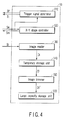
- FIG. 4 is a block view showing a configuration for functions of the computer 10.
- This computer 10 is comprised of a trigger signal generator 110 for receiving the encoder signal Se and outputting the trigger signal St and the flash signal Sf at prescribed timings, an X-Y stage controller 120 for receiving the encode signal Se and outputting the motor control signal Sm, an image reader 130 for receiving the image signal Si, a temporary memory 140 for temporarily storing image data Di, an image trimmer 150 for performing prescribed trimming processing on the image data Di, a large capacity memory 160 for saving trimmed image data Di' in order to perform probe mark checks afterwards, and a probe mark checking unit 170 for checking probe marks based on image data Di' stored in the large capacity memory 160.
- the probe mark checking unit 170 carries out probe mark checking after the photographing operation described below, but this operation is described later.
- the trigger signal generator 110 writes prescribed data to a prescribed address of the RAM 13 in advance and outputs the trigger signal St and the flash signal Sf at a prescribed timing based on the encoder signal Se.
- the following is a description of the operation with reference to FIG. 5.
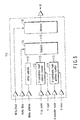
- FIG. 5 is a view illustrating an operation for generating the trigger signal St.
- the trigger signal generator 110 shown in FIG. 5 is equipped with a Y-coordinate read address counter 112, an X-coordinate read address counter 114, a selector 116, and memory 118, as functional structural elements relating to generation of the trigger signal St.
- the Y-coordinate read address counter 112 counts a pulse expressing the Y-pulse signal (Y-Up Pulse) and outputs the count value as a memory address signal (Y-coordinate address signal) corresponding to the Y-coordinate, and when a Y-reset signal (Y-Reset) is inputted, the count value is forcibly set as an address value corresponding to a prescribed Y-coordinate corresponding to the reference position in the Y-direction.
- the X-coordinate read address counter 114 counts a pulse expressing the X-pulse signal (X-Encoder Pulse) and outputs the count value as a memory address signal (X-coordinate address signal) corresponding to the X-coordinate, and when an X-reset signal (X-Reset) is inputted, the count value is forcibly set as an address value corresponding to a prescribed X-coordinate corresponding to the reference position in the X-direction.
- the Y-coordinate address signal and the X-coordinate address signal outputted from the Y-coordinate read address counter 112 and the X-coordinate read address counter 114 are inputted to the selector 116.
- a signal (hereafter referred to as "write address signal”) expressing a write address (write Address) corresponding to a coordinate corresponding to the center of an electrode and data (hereafter referred to as "write DATA”)to be written to the write address are inputted to the selector 116.
- the selector 116 selects one of two types of address signal from the write address signal and a read address signal comprised of a Y-coordinate address signal and an X-coordinate address signal and provides the selected address signal to memory 118.
- the write address signal is selected at this time, the write data is also supplied to the memory 118 and the write data is written to an address expressed this write address signal at the memory 118.
- the read address signal is selected, data at an address expressed by this read address signal is read from the memory 118 and outputted from the trigger signal generator 110 as the trigger signal St.
- the trigger signal generator 110 having the above construction receives layout information Ia (for example, coordinate information etc. expressing the position of each electrode pads 92 in a prescribed coordinate system set with respect to the semiconductor chip 91) relating to the layout of the semiconductor chips 91 included at the semiconductor wafer 90 and the layout of the electrodes 92 from a wafer information memory 105 for storing information relating to the semiconductor wafer 90 provided externally to this probe mark reading device 1 and calculates coordinates (hereafter referred to as "center coordinates of pads”) corresponding to central positions of all of the electrodes 92 to be taken as photographing targets included in the semiconductor chip 91 based on this layout information Ia.
- layout information Ia for example, coordinate information etc. expressing the position of each electrode pads 92 in a prescribed coordinate system set with respect to the semiconductor chip 91
- layout information Ia for example, coordinate information etc. expressing the position of each electrode pads 92 in a prescribed coordinate system set with respect to the semiconductor chip 91
- layout information Ia for example, coordinate information etc. expressing
- the calculated coordinates are converted to respective corresponding memory addresses, and data (in this case "1") expressing the presence of a central coordinate for a pad is written to the address in the memory 118.
- data in this case "1" expressing the presence of a central coordinate for a pad is written to the address in the memory 118.
- the memory address is input to the selector 116 as a write address (Write Address), and write data (Write Data) of "1" is inputted to the selector 116.
- the selector 116 writes "1" to a corresponding address of the memory 118.
- the memory address is set to uniquely correspond to the X-coordinate.
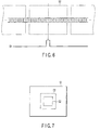
- FIG. 6 is a schematic view illustrating a relationship between this kind of photographing position and memory address.
- a square frame laid out along a straight line linking the central coordinates of the electrodes 92 shown in FIG. 6 in the X-direction represents a memory address, with numeric characters within the frame expressing data written to the memory address.
- "1" is written to an memory address corresponding to the central coordinate of the pad, and the trigger signal generator 110 outputs a trigger signal St when the photographing position coincides with a position corresponding to this address.
- a prescribed memory address corresponding to a Y-coordinate is set by the Y-coordinate read address counter 112 every time a Y-pulse signal included in the encoder signal Se from the X-Y stage 40 is inputted and is supplied to the selector 116. Further, when an X-reset signal is inputted, a prescribed memory address corresponding to the X-axis is set. Further, when the Y-reset signal is inputted, reading from the first position of the memory address is started.
- the memory address is incremented by the X-coordinate read address counter 114 every time the X-pulse signal is inputted, data is read in order from the memory address by the selector 116, and a trigger signal St is immediately output when a "1" is read.
- the electrode 92 is then photographed when the central coordinate of the pad coincides with the photographing position 20a.
- the time of photographing is the time that the flash signal Sf is outputted directly after outputting of the trigger signal St but both are substantially the same time and in reality there is no difference.
- all straight lines linking the central positions of each electrode 92 in the Y-direction is taken to be parallel to the Y-axis. Namely, the layout pattern in the X-direction for each of the electrodes 92 is taken to repeat in the Y-direction.
- the X-Y stage controller 120 receives the encoder signal Se indicating the position of the mounting table of the X-Y stage 40 on which the semiconductor wafer 90 is mounted, generates a prescribed motor control Signal Sm for moving the mounting stage to the prescribed position, and provides this motor control signal Sm to the X-Y stage 40.
- feedback control is carried out in such a manner as to move the mounting table of the photographing target position changing unit (for example, the X-Y stage) 40 so that the photographing position traces the locus shown by the arrow in this FIG. during photographing by the photographing unit (for example, the CCD camera) 20.
- This moving speed is a fixed speed and decided in such a manner as to move the photographing position 20a from the center position of a certain electrode to the center position of an electrode pads adjacent in the X-direction to the certain pad in the same amount of time or longer as the time (hereafter referred to as photographing time) required to acquire a single image when acquiring images consecutively in order using the CCD camera 20. If movement is achieved within a time shorter than the photographing time, then it is no longer possible to photograph (the central positions of) all of the electrodes.
- the photographing time is in the order of, for example, 30 milliseconds. Further, it is not necessary for the moving speed to be fixed, but when the moving speed is fixed, it is preferable for the photographing conditions at each photographing position 20a to be fixed.
- the image reader 130 receives the image signal Si obtained by the CCD camera 20 and generates and outputs image data Di that is an image photographed for the electrode and the vicinity of the electrode from this image signal Si.
- This image data Di is temporarily stored in a prescribed area of the RAM 13 by the temporary memory 140.
- the image trimmer 150 generates trimmed image data Di' by performing trimming on the image data Di stored by the temporary memory 140 so as to delete prescribed areas of the photographed image to the outside of the vicinity of the electrode 92.
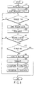
- FIG. 7 is a schematic view illustrating this trimming processing.
- An image 51 in FIG. 7 corresponds to the image data Di and the central coordinate of the electrode 92 coincides with the photographing position 20a.
- a trimming boundary line 52 shown by the dashed line in FIG. 7 includes the image photographed for the electrode 92 and is set as a boundary line encompassing a region slightly larger than the periphery of the electrode 92.
- a central position of the region within the trimming boundary line 52 is set to coincide with the central coordinate of the electrode 92. It is therefore straightforward to set the trimming boundary line 52 with respect to the image 51.
- Trimmed image data Di' is therefore easily created from an image taken for the electrode 92 within the trimming boundary line 52 without it being necessary to perform trimming processing by recognizing the image taken for the electrode 92 using well-known image recognition processing methods.
- the trimmed image data Di' is saved to the hard disc 16 by the large capacity memory 160 via the disc interface 15.
- the image data Di' saved by the large capacity memory 160 is then taken as the subject of probe mark checking by the probe mark checking unit 170.
- the following is a description with reference to the drawings of a processing procedure relating to the operation for photographing of the computer 10 corresponding to the above functions.
- FIG. 8 is a flowchart showing the processing procedure relating to a photographing operation for the computer 10.
- the trigger signal generator 110 that is a function of the computer 10 carries out initial setting processing to receive layout information Ia relating to the layout of the semiconductor chips 91 included at the semiconductor wafer 90 and the layout of the electrodes 92 etc. from the wafer information memory 105, calculate center coordinates for all of the electrodes 92 included in the semiconductor chip 91, convert the calculated coordinates into corresponding memory addresses, and write data "1" indicating the presence of a central coordinate of a pad in the memory address (step S10). Center coordinates for all of the electrodes 92 included in all of the semiconductor chips may then be calculated and written to corresponding memory addresses.
- the X-Y stage controller 120 generates a prescribed motor control signal Sm in order to move the position of the mounting table of the X-Y stage 40 on which the semiconductor wafer 90 is mounted in order to align the photographing position 20a of the CCD camera 20 with a prescribed start position 21 and provides this motor control signal Sm to the X-Y stage 40. Further, when the photographing position 20a of the CCD camera 20 is aligned with the prescribed start position P1, the prescribed motor control signal Sm is provided to the X-Y stage 40 in order to move the mounting table at the fixed aforementioned speed of movement in the X-direction based on the consecutively received encoder signals Se expressing the position of the mounting table (step S20).
- the trigger signal generator 110 determines whether or not the center coordinate of the pad coincides with the photographing position 20a based on the encoder signal Se (step S30). When there is no coincidence, the determination of step S30 is repeated. When there is coincidence, the trigger signal generator 110 outputs a trigger signal St (step S40). Outputting of the flash signal Sf directly after outputting of the trigger signal St is then as described above.
- the image reader 130 receives the image signal Si obtained by the CCD camera 20, generates image data Di that is an image photographed for the electrode and the vicinity of the electrode from this image signal Si, and the temporary memory 140 temporarily stores this image data Di (step S50).
- the X-Y stage controller 120 makes a determination as to whether or not image reading in the X-direction is complete due to the photographing position 20a of the CCD camera 20 exceeding the center coordinate of the electrode 92 at the furthermost end based on the encoder signal Se (step S60). If this is not the case, the processing returns to step S30, the process of sending a trigger signal at the time of a trigger is repeated until the image reading in the X-direction is complete (step S60 ⁇ S30 ⁇ S40 ⁇ S50 ⁇ S60). When image reading in the X-direction is complete, a determination is made as to whether or not the photographing position 20a has reached the end position P2 (step S70).
- step S30 is returned to after carrying out a process from step S80 to S110 described below, and the process is repeated until the photographing position 20a reaches the end position P2 (S70 ⁇ S80 ⁇ S90 ⁇ S100 ⁇ S110 ⁇ S30 ⁇ S40 ⁇ S50 ⁇ S60 ⁇ S70) .
- P2 S70 ⁇ S80 ⁇ S90 ⁇ S100 ⁇ S110 ⁇ S30 ⁇ S40 ⁇ S50 ⁇ S60 ⁇ S70
- the X-Y stage controller 120 When a determination is made in the process in step S70 that the photographing position 20a has not reached the end position P2, the X-Y stage controller 120 generates a prescribed motor control signal Sm and provides this signal to the X-Y stage 40 in order to move the position of the mounting table of the X-Y stage 40 mounted with the semiconductor wafer 90 so that the photographing position 20a of the CDD camera 20 lines up with the Y-coordinate corresponding to the line for the following electrode (step S80).
- the image trimmer 150 generates trimmed image data Di' by performing trimming on the image data Di stored by the temporary memory 140 so as to cut-out prescribed areas other than the area including the image photographed for the electrode 92 (step S90).
- This trimming process is carried out collectively for all of the image data Di (specifically, images taken for all of the electrodes 92 laid-out in the X-direction) stored by the temporary memory 140.
- the image trimmer 150 creates data for the trimmed image data Di' that is added with supplemental information including prescribed numbers and comments utilized by the probe mark checking unit 170 when checking probe marks (step S100). Further, the large capacity memory 160 stores the data with the supplemental information added by the image trimmer 150 (step S110). After this, the above processing returns to step S30 and the processing is repeated until the photographing position 20a reaches the end position P2.
- steps S90 to S110 can be carried out using the moving time for moving the position of the mounting table of the X-Y stage 40 in the processing of step S80.
- steps S90 to S110 can be carried out using the moving time for moving the position of the mounting table of the X-Y stage 40 in the processing of step S80.
- a configuration can be adopted where these processes are carried out immediately after the image capture processing of step S50. These processes may also be carried out concurrently with the processing of step S80 (and processes executed thereafter).
- step S60 When it is determined in step S60 that the photographing position 20a has reached the end position P2, the image capture operation for the semiconductor chip is complete. Further, when there is a semiconductor chip for which images are to be read-in present, the above processing is started from the beginning after completion of the probe mark checking operation described in the following.
- FIG. 11 is a flowchart showing the overall processing procedure when carrying out probe mark checking in this embodiment.
- photographing image processing for model registration
- step S1 photographing (image processing for model registration) is carried out in order to register probe marks as models formed under ideal conditions on all of the electrode included at a prescribed semiconductor chip.
- the prescribed test probe for example, in the case of a new product
- a probe mark is formed using a prescribed test probe on a dummy wafer that as yet has no probe marks, or on a new chip.
- the positions etc. of probe marks formed in this manner are therefore substantially ideal with no abnormalities.
- step S2 processing (model registration processing) is carried out to calculate and save barycentric coordinates for probe marks constituting the model by analyzing the images for the electrodes including the probe marks constituting the models obtained by image processing for model registration (step S1).
- Publicly known methods are used to calculate barycentric coordinates using this kind of image analysis. For example, the region occupied by the probe mark included in the image or the pixels constituting the boundary are detected based on luminance of the pixels and the barycentric coordinates of the probe marks are calculated based on the coordinates of the pixels.
- the barycentric coordinates are coordinates in a prescribed coordinate system preset with respect to the semiconductor chip 91. The manner in which layout information Ia including in the information relating to this coordinate system is stored in the wafer information memory 105 is described above.
- the barycentric coordinates are calculated for all of the probe marks and are stored in the large capacity memory 160 together with information such as prescribed numbers utilized at the time of probe-mark checking due to the probe mark checking unit 170.
- various calculations are carried out based on barycentric coordinates for the probe marks but coordinates for characteristic points expressing included properties that are common to all of the probe marks (such as, for example, minimum Y-coordinate image coordinates, etc.) may also be used in place of the barycentric coordinates.
- step S1 and step S2 Information obtained through the processing of step S1 and step S2 can be used repeatedly until the prescribed test probe exhibits abnormality. To this end, it will suffice to carry out these processes once the test probe has been used, etc.
- the prescribed test probe will be mounted at any one of a plurality of test devices, a configuration is preferable where the information is shared by the plurality of test devices via a prescribed network, etc.
- step S3 photographing (image processing for use in difference operations) of the electrodes included at the semiconductor chip 91 before a probe test is carried out.
- This image processing may be carried out for all of the electrodes included at a prescribed semiconductor chip 91 or may be carried out for only the four electrodes arranged in the vicinity of the corners of the semiconductor chip 91. This may also be carried out for all of the electrodes of the semiconductor chips included on the semiconductor wafer 90. It is possible to detect only probe marks formed by the final probe test even when a plurality of probe marks are formed at a single electrode by performing difference operations on images obtained by the image processing and images for after a plurality of probe tests.
- a difference operation is not carried out for all of the electrodes but a description is given later with respect to the details of the content.
- the electrode images obtained by this difference operation image processing can be used in detailed check of the probe marks (step S7 described later), so that when utilized in a detailed check, it is preferable to carry out the above photographing processing on all of the semiconductor chips.
- step S4 probe testing is carried out on all of the semiconductor chips included in a prescribed semiconductor wafer 90 using a prescribed probe test device installed with the prescribed test probe. Probe marks to be taken as targets of probe mark testing are formed by the probe tests.
- step S5 photographing (image processing for use in probe mark checks) of electrodes including probe marks formed by the probe tests is carried out by the probe mark reading device.
- This operation is the above photographing operation described with reference to FIG. 8 etc.
- step S6 prescribed probe mark checking processing is carried out based on electrode images obtained in image processing for use in probe mark checks (step S5). The detailed contents of this process are described in the following.
- step S7 A further detailed check is carried out in step S7 based on results obtained in step S6 (probe mark checking processing). For example, an image for an electrode, including a probe mark determined to be defective by the probe mark checking process is read from the large capacity memory 160 and a detailed analysis of the shape and size of the probe mark etc. is performed. This detailed check is typically carried out under the observation of an operator. This detailed check may be omitted if necessary.
- FIG. 12 is a flowchart showing the processing procedure relating to a probe mark checking operation of the computer 10.
- a probe mark checking unit 170 that is one function implemented by the computer 10 carries out initial vector calculation processing (step S210) to calculate a vector (hereinafter referred to as "initial vector") indicating the extent to which the position of the probe mark formed due to the probe test differs from the position of the probe mark registered as a model (step S210).
- initial vector a vector
- FIG. 13 is a flowchart showing the procedure for this subroutine.
- the probe mark checking unit 170 reads out image data for the corners of images of electrodes obtained in the probe mark checking image processing (step S5), i.e. reads out data for four electrodes (hereafter referred to as "corner pads") arranged in the vicinity of the four corners from the large capacity memory 160 (step S211).
- the probe mark checking unit 170 detects the probe mark formed due to the probe test from the images for the corner pads obtained in step S211 (step S212).
- the probe mark formed by the probe test is detected by performing a difference operation between the images of the corner pads obtained in step S211 and the images for the corner pads before this probe test obtained in the image processing for use in difference operations (step S3).
- FIG. 14 is a view illustrating this difference operation. Image A in FIG.
- FIG. 14 shows an image for a corner pad for before a probe test and image B of FIG. 14 shows an image for a corner pad after a probe test. If a difference operation is then performed between image B and image A, portions that are common to both images shown by the dashed line in image C are deleted so that, as shown in image C, an image only for a corner pad including only a probe mark formed by the probe test on this occasion is obtained. This probe mark is referred to as a corner probe mark.
- the probe mark checking unit 170 calculates barycentric coordinates for the corner probe mark from an image for the corner pad including the corner probe mark obtained in step S212 (step S213).
- the well-known method for calculating these barycentric coordinates is described above for the model registration processing (step S2) and the fact that the barycentric coordinates are coordinates of a prescribed coordinate system preset in the semiconductor chip 91 is also described above.
- the probe mark checking unit 170 calculates a barycentric coordinate central position Ci from the barycentric coordinates for the corner probe marks obtained in step S213 (step S214).
- the barycentric position of the probe mark does not always coincide with the central position of an electrode and the central position Ci is therefore the vicinity for which there is no coincidence with the central position of the semiconductor chip 91.
- the probe mark checking unit 170 calculates a barycentric coordinate central position Cm from the barycentric coordinates for the model corner probe marks read in step S215 (step S216).
- This central position Cm is the vicinity where the central position of the semiconductor chip 91 and the central position Ci do not coincide.
- the probe mark checking unit 170 calculates a vector (hereafter referred to as "initial vector") drawn from the central position Cm calculated in step S216 to the central position Ci calculated in step S214. (step S217).
- This initial vector can then be used in the following processing as a vector indicating shifts from the probe mark registered as a model to a probe mark formed by the probe test.
- FIG. 15 is a schematic view illustrating initial vector calculation.
- a semiconductor chip 910 shown in FIG. 15 has six electrodes 921 to 926 and these electrodes include probe marks 931 to 936 formed by a probe test.
- the probe marks 831 to 836 registered as models corresponding to these probe marks are shown by the dotted lines in FIG. 15 and the barycentric positions of the probe marks are shown by cross-marks.
- An intersection point of a line connecting barycentric positions of the corner probe marks 933 and 934 of the semiconductor chip 910 and a line connecting barycentric positions of the corner probe marks 931 and 936 is taken as a central position Ci of these probe marks.
- an intersection point of a line connecting barycentric positions of model corner probe marks 833 and 834 and a line connecting barycentric positions of model corner probe marks 831 and 836 is taken as a central position Cm of these probe marks.
- An initial vector Vi that is a vector going from the central position Cm to the central position Ci is not completely the same as vectors from the barycentric positions of the model corner probe marks 831, 833, 834 and 836 to the barycentric positions of the corresponding corner probe marks 931, 933, 934 and 936.
- the reason for this is that the (for example, new) test probe forming the probe marks taken as models has an ideal arrangement and vectors indicating directions of shifting of the test probe should all be the same and should be equal to the initial vectors.
- a test probe used a number of times in probe tests may become bent, chipped or worn etc. due to age deterioration so that the arrangement may shift from the ideal.
- the initial vector described above is calculated taking note of corner probe marks in order to average out shifts in the direction of rotation and other shifts. It is preferable to calculate vectors from probe marks taken as models for all of the electrodes to probe marks formed by the probe test in order to completely average out the shifts.
- the initial vectors are calculated using the central position Ci and the central position Cm.
- the probe mark checking unit 170 carries out determination range calculation processing in order to determine the quality of the probe marks (step S220).
- the probe marks formed at the electrode pads by the probe test are positioned in a vicinity that is in a direction and distance shown by the initial vector from the probe mark taken as a model.
- the range indicating the limit that can be said to be this vicinity is referred to here as the determination range.
- FIG. 16 is a schematic view illustrating an amount of shift due to a first probe P1
- FIG. 17 is a schematic view illustrating an amount of shift due to a second probe P2.
- Ra shows an extent of shifting of probe mark positions formed by the first and second probes P1 and P2 of different shapes, with a dotted line showing the range of this shifting.
- This amount of shifting Ra can be obtained in advance using numerical calculations from the amount of flexing and bending based on the shape of the first and second probes P1 and P2, rigidity of metal constituting this material, and applied load, etc.
- RM in the drawings shows the maximum amount of shift in all of the probe mark positions formed by all of the test probes used when the first and second probes P1 and P2 are taken as model test probes.
- This amount of shift RM can easily be obtained from the positions of all of the probe marks registered as models. For example, it is possible to consider calculating a difference between a respective minimum value and maximum value for an X-coordinate and a Y-coordinate for barycentric coordinates for a probe mark registered as a model, divide values for which this difference is larger by two to give a value, and then take this value with Ra added as RM.
- the amount of shift RM being bigger than the amount of shift Ra depends on the presence of slight variations in the shape etc. of each test probe and the presence of slight variations in a fitting position varying slightly from a calculated position.
- RT in the drawings shows the maximum amount of shift in all of the probe mark positions formed by all of the test probes taking into consideration shifts occurring due to age deterioration due to carrying out a plurality of probe tests.
- This amount of shift RT can easily be obtained from all of the positions of probe marks actually formed but this is troublesome and takes a great deal of time as it requires a great deal of calculation and involves a substantial amount of processing. It goes without saying that it is preferable to detect the probe marks at high speed.
- the amount of shift RT is calculated by multiplying the amount of shift RM by a prescribed coefficient larger than 1 obtained taking into consideration experience of the influence of age deterioration. This may also be calculated taking into consideration the amount of shift of the four corner probe marks.
- the determination range of the probe mark checking unit 170 has a determination range that is a circle with the calculated shift amount RT as a radius.
- the probe mark checking unit 170 reads images for electrodes taken as targets of a probe mark check from the large capacity memory 160 (step S230).
- the probe mark checking unit 170 carries out processing to determine quality of probe marks included in the read-out electrode images (step S240). A description of the details of the processing (subroutine) for this quality determination process will now be described.
- FIG. 18 is a flowchart showing the procedure for this subroutine.
- the probe mark checking unit 170 reads out from the large capacity memory 160 barycentric coordinates for probe marks pre-registered as models corresponding to the electrodes read out in step S230 (step S241).
- the probe mark checking unit 170 calculates coordinates for a point in a direction and distance specified by the initial vector calculated in step S230 from the barycentric positions of the probe marks taken as models read out in step S230. Ideally, it is preferable to set the determination range taking this point as center because there is a barycentric coordinate for the probe mark formed by a probe test in the vicinity of this point (the center coordinate).
- the probe mark checking unit 170 sets the determination range as a circle taking the amount of shift RT calculated in step S220 as a radius and taking the center coordinate of the determination range calculated in step S242 as center (step S243).
- the determination range is taken to be a circle but any kind of shape such as a square, etc. is also possible.
- the probe mark checking unit 170 detects probe marks from a prescribed region of the electrode image within the determination range set in step S243 (step S243).
- Well known image processing methods such as detection methods based on pixel luminance etc. can be used in detection of probe marks. It is therefore not necessary to check the whole of the image for the electrodes because in this embodiment, only probe marks for a prescribed region within the determination range are detected. It is therefore possible to detect probe marks at high speed.
- the probe mark detecting unit 170 determines whether or not probe marks are detected in step S243 (step S244). When a probe mark is detected, the probe mark is determined to be good, the determination results are stored in memory 10a etc. and the processing of FIG. 12 is returned to (step S244). When a probe mark is not detected, the probe mark is determined to be bad, the determination results are stored in memory etc. and the processing of FIG. 12 is returned to (step S245). In step S244, when part of a probe mark is detected within the determination range, this is handled as though a probe mark is not detected because the whole of the probe mark cannot be detected.
- FIG. 19 is a view showing an example of probe mark detection in probe mark quality determination processing.
- An image 927 of an electrode shown in FIG. 19 includes a probe mark 937 formed by a probe test on a current occasion and probe marks 957a, 957b and 957c formed by probe tests on a previous occasion and beforehand. Further, the probe mark 837 registered as a model corresponding to the probe mark 937 is shown by the dotted lines in FIG. 15 and the barycentric positions of the probe marks are shown by cross-marks.
- probe mark 937 is present within a circle of radius RT from the center coordinate of the determination range and a probe mark is detected from the image within the circular determination range. A determination is therefore made that the probe mark 937 is good.
- FIG. 20 is a view showing a further example of probe mark detection in probe mark quality determination processing.
- Each of the elements in FIG. 20 which is the same as in FIG. 19, is given the same numeral, and description thereof is omitted.
- the example shown in FIG. 20 differs from the example shown in FIG. 19 in that probe mark 937 is present outside a circle of radius RT from the center coordinate of the determination range and a probe mark is therefore not detected from the image within the circular determination range. A determination is therefore made that the probe mark 937 is poor.
- the probe mark checking unit 170 omits the process of step S260 when the probe mark is poor and carries out the process of step S270, and when the probe mark is good, carries out the process of step S260 (step S250).
- the probe mark detecting unit 170 carries out a probe mark position determination process to determine whether or not the probe mark position is good for each probe mark that is determined to be good (step S260).
- a protective part (passivation part) is normally formed in the vicinity of the edge of an electrode and problems such as conduction defects etc. may therefore occur in the probe test when the region occupied by the probe mark overlaps with the region for the protective part. It is therefore necessary to determine that the probe mark position is poor when this kind of overlapping occurs.
- maximum and minimum values are calculated for the X-coordinate and Y-coordinate of the probe mark and quality of the probe mark position is then determined by determining whether or not these coordinates fall within the region of the protective part.
- FIG. 21 is a view showing maximum values and minimum values for X-coordinates and Y-coordinates of probe marks.
- Xmax shows the maximum value of the X-coordinate of the probe mark
- Xmin shows the minimum value of this X-coordinate
- Ymax shows the maximum value of the Y-coordinate
- Ymin shows the minimum value of the Y-coordinate.
- the image 927 of the electrode shown in FIG. 21 has a protective part formed in the vicinity of the edge. However, none of Xmax, Xmin, Ymax and Ymin fall within the protective part and the region occupied by the probe mark 937 can therefore be determined not to overlap with this protective part.
- FIG. 22 is a view showing a borderline for determining this extent of proximity.
- the probe mark When the value is a coordinate corresponding to inside of the first borderline 901 but is a coordinate corresponding to outside of a second borderline 902, the probe mark does not overlap with the protective part but is relatively close and the probe mark position is determined to require further investigation.
- the probe mark When the value is a coordinate corresponding to inside of the second borderline 902, the probe mark is distanced from the protective part and the probe mark position is determined to be good. The results of this determination (poor, requires further investigation, good) are stored temporarily in memory etc.
- the probe mark determination unit 170 performs processing to make a prescribed classification header based on each of the determination results temporarily stored in memory etc.
- the classification header may include, for example, test date, tester number, probe model (model probe mark) number, wafer product name, wafer lot number, chip number, pin (electrode) number, probe determination (probe quality determination) results, probe position determination results, and prescribed probe mark detection parameters, etc.
- the probe determination (probe mark quality determination) results include data indicating "good” or "poor” as results obtained in the probe mark quality determination process (step S240) and a shift amount RT obtained in the determination range calculation process (step S220).
- the probe position determination process includes data indicating "poor”, “requires further investigation”, and "good” obtained in the probe mark position determination process (step S260).
- Prescribed probe mark determination parameters may include barycentric coordinates for a probe mark, and Xmax, Xmin, Ymax and Ymin values, and may further include area and aspect ratio of the probe mark obtained through prescribed calculations.
- the classification header including the above content correlated with image files of the electrodes is stored in (a prescribed folder etc. of) the large capacity memory 160. By using this classification header, images of electrodes to be checked can be efficiently designated and read out during detailed checks (step S7) carried out afterwards.
- the probe mark detecting unit 170 reads out images for all of the electrodes included in the semiconductor chip 91 and determines whether or not checking has been performed (step S280). When all of the images are not read out, in order to read out an image for the next electrode, the process of step S230 is returned to, and the above processing is repeated until all of the images are read out (S230 ⁇ S240 ⁇ 5250 ⁇ (S260) ⁇ S270 ⁇ S280 ⁇ S230). When all of the images are read out, checks for all of the probe marks included in the semiconductor chip 91 are complete.
- step S210 to step S270 photographing of the electrodes included in the next semiconductor chip included in the semiconductor wafer 90 takes place, and then the same processing as described above (step S210 to step S270) is commenced in order to check probe marks on the electrodes. This process is then repeated until photographing and probe mark checking are complete for all of the semiconductor chips included in the semiconductor wafer 90.
- the probe mark checking operation of the computer 10 including the above processing is carried out after completion of the photographing operation for the electrodes of the semiconductor chip but if the processing speed of the computer 10 is sufficiently high, it is also possible to carry out the probe mark checking operation for each pad every time a single electrode is photographed. These operations may also be carried out concurrently.
- the probe mark reading device 1 moves the semiconductor wafer 90 mounted on the mounting table in the X-direction at a fixed speed using the X-Y stage 40, with pictures being taken in order of the electrodes lit up by bursts of light from the light source 30 by the CCD camera 20.
- the probe mark reading device 1 is capable of acquiring images for electrodes and read probe marks without putting a user to any trouble and in a short period of time.
- the probe mark reading device 1 is configured so as to photograph electrodes lit up for a short period of time by bursts of light from the light source 30 in order using the CCD camera 20.
- the probe mark reading device is capable of ensuring that images taken do not blur and also that images can be captured with a device configuration that is straightforward and inexpensive compared with control using devices having physical shutters, etc.
- the trigger signal generator 110 included in this probe mark reading device calculates coordinates corresponding to central positions of all of the electrodes to be photographed based on layout information Ia relating to the layout of the semiconductor chips 91 stored in the wafer information memory 105 and the layout of the electrodes 92 etc. As a result, it is possible to read a multiplicity of probe marks formed at a multiplicity of electrodes which are by no means arranged at equal intervals and for which the possibility of the layout position changing depending on the semiconductor wafer exists at high speed.
- the probe mark reading device carries out time-consuming difference operations for images only when calculating initial vectors, with determination of quality of the probe marks in other probe mark checks then being carried out based on initial vectors and prescribed determination range (shift amount RT). It is therefore possible to determine probe mark quality and probe mark position of probe marks formed by a final probe test at a high speed even in cases where a plurality of probe marks are included in the image taken for an electrode. For example, if difference operations are to be carried out of subtracting the images for before a probe test from the images for one thousand electrodes (i.e.
- the time required to perform one difference operation is approximately 200 milliseconds and the time required to read out one image for before the final probe test is in the order of 30 milliseconds.
- the time required to read all of the probe marks is therefore in the order of 230 seconds (approximately four minutes).
- the probe mark checking of this embodiment is carried out on images for one thousand electrodes, the time required to detect one probe mark is in the order of 10 milliseconds and a check of all the probe marks is completed in ten seconds. It can therefore be understood that the probe mark checking of this embodiment can be carried out at extremely high speed. Further, according to a difference operation in pixel units, there is the possibility of erroneous detections etc.
- reliable probe mark checks can be carried out without being influenced by shifting at the time of image acquisition or changes in pixel luminance etc. because relative position detection is carried out based on an initial vector.
- the central coordinates and photographing position 20a for the (images 51 including images taken for the) electrodes 92 coincide.
- a configuration is adopted having just a single electrode 92 included in the image data Di but the number of electrodes 92 to be photographed once may also be multiple.
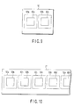
- FIG. 9 is a view showing an example of an image 51 including images taken for two electrodes 92a and 92b with this configuration.
- the central positions of the regions within trimming borderlines 52a and 52b corresponding to the electrodes 92a and 92b can then easily be calculated from the layout information Ia relating to the layout etc. of the electrodes 92a and 92b indicated by the wafer information memory 105. It is therefore straightforward to set trimming boundary lines 52a and 52b with respect to the image 51. Trimmed image data Di' is therefore easily created from an image taken for electrodes 92a and 92b within trimming boundary lines 52a and 52b without it being necessary to perform trimming processing by recognizing the image taken for the electrode 92a and 92b using well-known image recognition processing.
- FIG. 10 is a view showing an example of an image 51 including images taken for four and a half electrodes 92a to 92e.
- Central positions of trimming borderlines 52a to 52e corresponding to images taken for the electrodes 92a to 92e can easily similarly be calculated from layout information Ia relating to the arrangement of electrodes etc. indicated by the wafer information memory 105.
- a plurality of trimmed image data Di' composed of images taken for the electrodes 92a to 92e within the trimming borderlines 52a to 52e can then easily be made.
- the image for the electrode 92e is discarded because the whole of the pad is not photographed but a configuration where the whole of the image is created by synthesis with the remaining portion of the image taken next is also possible.
- the probe mark reading device is capable of acquiring images for electrodes and read probe marks in a still shorter period of time.
- the plurality of photographed electrodes are adjacent to each other in the X-direction as shown in FIG. 10.
- the light source 30 lights up the prescribed portion by generating a high-intensity burst of light for just a short time of a few microseconds from the time of being provided with a flash signal Sf so as to enable the CCD camera 20 to acquire a photographed image with no blurring.
- the shutter device may also be implemented electronically.
- the light source 30 is by no means limited to a flash such as, for example, a xenon flash lamp. It is also possible to adopt a configuration where the X-Y stage 40 is controlled in such a manner that the speed of movement before moving to the electrodes at the photographing position is slowed down in order to take images using the CCD camera 20 that are not blurred. However, the average speed will become slower with this configuration due to repeated acceleration and deceleration. The above embodiment is therefore more preferable when movement takes place at a fixed fast speed.
- a configuration is adopted where a photographing position 20a is consecutively moved by moving the position of a semiconductor wafer 90 to be photographed using an X-Y stage 40.
- a camera moving device or camera oscillating device where the photographing position 20a is moved in the X-direction or Y-direction by changing the position or photographing angle of the CCD camera 20 could also be provided.
- a reflection angle changing device where a reflecting mirror is arranged and the X-Y stage omitted so that an image of the electrode 92 is provided to the CCD camera 20 via the reflecting mirror, with the photographing position of the CCD camera 20 then being changed in the X-direction and the Y-direction by changing the angle of the reflecting mirror.
- a configuration where photographing positions are consecutively moved to as a result of an appropriate combination of these configurations is also possible.
- a configuration is adopted where electrodes 92 included on a single semiconductor chip of a semiconductor wafer 90 are photographed in order but it is also possible to photograph the whole of the semiconductor wafer 90 in order. Namely, it is also possible to photograph electrodes 92 included on a plurality of semiconductor chips during photographing in the X-direction in order. In the case of this kind of photographing, which photographed electrodes correspond to which semiconductor chip can easily be determined based on the layout information Ia relating to layout etc. of the semiconductor chips indicated by the wafer information memory 105.
- feedback control can be carried out based on the encoder signal Se from the X-Y stage 40.
- this encoder signal Se without basing control on this encoder signal Se, in cases where reliable determination of a position where the mounting table of the X-Y stage 40 is intended to be is possible using the X-Y stage controller 120, it is also possible to carry out control based on this intended position.
- a probe mark checking operation is carried out on images for electrodes obtained by consecutively taking pictures of a semiconductor wafer 90 on (a mounting table of) an X-Y stage 40 moving at a fixed speed using a CCD camera 20.
- images taken of electrode pads it is sufficient for images taken of electrode pads to exist in order to implement the probe mark checking operation. It is by no means necessary to carry out the aforementioned photographing operation as a prerequisite of the probe mark checking operation and, for example, images or electrodes may be acquired using a related photographing operation. Images for electrodes taken by a different device to this device may then be provided to this device, so that probe mark checking is carried out based on these provided images.
- the embodiment as described above may also be applied to probe mark test devices for performing just probe mark checking operations.
Landscapes
- Engineering & Computer Science (AREA)
- Physics & Mathematics (AREA)
- General Physics & Mathematics (AREA)
- Computer Vision & Pattern Recognition (AREA)
- Computer Hardware Design (AREA)
- Microelectronics & Electronic Packaging (AREA)
- General Engineering & Computer Science (AREA)
- Health & Medical Sciences (AREA)
- Electromagnetism (AREA)
- Toxicology (AREA)
- Quality & Reliability (AREA)
- Theoretical Computer Science (AREA)
- Testing Or Measuring Of Semiconductors Or The Like (AREA)
- Testing Of Individual Semiconductor Devices (AREA)
Applications Claiming Priority (5)
| Application Number | Priority Date | Filing Date | Title |
|---|---|---|---|
| JP2002312579 | 2002-10-28 | ||
| JP2002312579 | 2002-10-28 | ||
| JP2003194541 | 2003-07-09 | ||
| JP2003194541 | 2003-07-09 | ||
| PCT/JP2003/013256 WO2004038786A1 (ja) | 2002-10-28 | 2003-10-16 | プローブ痕読取装置およびプローブ痕読取方法 |
Publications (2)
| Publication Number | Publication Date |
|---|---|
| EP1557876A1 true EP1557876A1 (de) | 2005-07-27 |
| EP1557876A4 EP1557876A4 (de) | 2009-06-24 |
Family
ID=32109511
Family Applications (1)
| Application Number | Title | Priority Date | Filing Date |
|---|---|---|---|
| EP03754153A Withdrawn EP1557876A4 (de) | 2002-10-28 | 2003-10-16 | Sondenmarkierungsleser und sondenmarkierungsleseverfahren |
Country Status (6)
| Country | Link |
|---|---|
| US (2) | US7026832B2 (de) |
| EP (1) | EP1557876A4 (de) |
| KR (1) | KR100738693B1 (de) |
| AU (1) | AU2003273025A1 (de) |
| TW (1) | TW200423276A (de) |
| WO (1) | WO2004038786A1 (de) |
Cited By (2)
| Publication number | Priority date | Publication date | Assignee | Title |
|---|---|---|---|---|
| WO2016033232A1 (en) * | 2014-08-26 | 2016-03-03 | Deca Technologies Inc. | Front side package-level serialization for packages comprising unique identifiers |
| CN111742233A (zh) * | 2018-02-26 | 2020-10-02 | 雅马哈精密科技株式会社 | 定位装置及定位方法 |
Families Citing this family (76)
| Publication number | Priority date | Publication date | Assignee | Title |
|---|---|---|---|---|
| US5345170A (en) | 1992-06-11 | 1994-09-06 | Cascade Microtech, Inc. | Wafer probe station having integrated guarding, Kelvin connection and shielding systems |
| US6380751B2 (en) | 1992-06-11 | 2002-04-30 | Cascade Microtech, Inc. | Wafer probe station having environment control enclosure |
| US6232789B1 (en) * | 1997-05-28 | 2001-05-15 | Cascade Microtech, Inc. | Probe holder for low current measurements |
| US5561377A (en) | 1995-04-14 | 1996-10-01 | Cascade Microtech, Inc. | System for evaluating probing networks |
| US5729150A (en) * | 1995-12-01 | 1998-03-17 | Cascade Microtech, Inc. | Low-current probe card with reduced triboelectric current generating cables |
| US5914613A (en) * | 1996-08-08 | 1999-06-22 | Cascade Microtech, Inc. | Membrane probing system with local contact scrub |
| US6002263A (en) | 1997-06-06 | 1999-12-14 | Cascade Microtech, Inc. | Probe station having inner and outer shielding |
| US6034533A (en) * | 1997-06-10 | 2000-03-07 | Tervo; Paul A. | Low-current pogo probe card |
| US6256882B1 (en) | 1998-07-14 | 2001-07-10 | Cascade Microtech, Inc. | Membrane probing system |
| US6578264B1 (en) * | 1999-06-04 | 2003-06-17 | Cascade Microtech, Inc. | Method for constructing a membrane probe using a depression |
| US6445202B1 (en) | 1999-06-30 | 2002-09-03 | Cascade Microtech, Inc. | Probe station thermal chuck with shielding for capacitive current |
| US6838890B2 (en) * | 2000-02-25 | 2005-01-04 | Cascade Microtech, Inc. | Membrane probing system |
| US6914423B2 (en) | 2000-09-05 | 2005-07-05 | Cascade Microtech, Inc. | Probe station |
| US6965226B2 (en) | 2000-09-05 | 2005-11-15 | Cascade Microtech, Inc. | Chuck for holding a device under test |
| DE10143173A1 (de) | 2000-12-04 | 2002-06-06 | Cascade Microtech Inc | Wafersonde |
| WO2003052435A1 (en) * | 2001-08-21 | 2003-06-26 | Cascade Microtech, Inc. | Membrane probing system |
| WO2003020467A1 (en) | 2001-08-31 | 2003-03-13 | Cascade Microtech, Inc. | Optical testing device |
| US6777964B2 (en) | 2002-01-25 | 2004-08-17 | Cascade Microtech, Inc. | Probe station |
| US6951846B2 (en) * | 2002-03-07 | 2005-10-04 | The United States Of America As Represented By The Secretary Of The Army | Artemisinins with improved stability and bioavailability for therapeutic drug development and application |
| JP2005527823A (ja) | 2002-05-23 | 2005-09-15 | カスケード マイクロテック インコーポレイテッド | デバイスのテスト用プローブ |
| US6847219B1 (en) | 2002-11-08 | 2005-01-25 | Cascade Microtech, Inc. | Probe station with low noise characteristics |
| US6724205B1 (en) | 2002-11-13 | 2004-04-20 | Cascade Microtech, Inc. | Probe for combined signals |
| US7250779B2 (en) | 2002-11-25 | 2007-07-31 | Cascade Microtech, Inc. | Probe station with low inductance path |
| US6861856B2 (en) | 2002-12-13 | 2005-03-01 | Cascade Microtech, Inc. | Guarded tub enclosure |
| US7221172B2 (en) | 2003-05-06 | 2007-05-22 | Cascade Microtech, Inc. | Switched suspended conductor and connection |
| US7492172B2 (en) | 2003-05-23 | 2009-02-17 | Cascade Microtech, Inc. | Chuck for holding a device under test |
| US7057404B2 (en) | 2003-05-23 | 2006-06-06 | Sharp Laboratories Of America, Inc. | Shielded probe for testing a device under test |
| US7250626B2 (en) | 2003-10-22 | 2007-07-31 | Cascade Microtech, Inc. | Probe testing structure |
| DE202004021093U1 (de) | 2003-12-24 | 2006-09-28 | Cascade Microtech, Inc., Beaverton | Aktiver Halbleiterscheibenmessfühler |
| US7187188B2 (en) | 2003-12-24 | 2007-03-06 | Cascade Microtech, Inc. | Chuck with integrated wafer support |
| JP2008502167A (ja) | 2004-06-07 | 2008-01-24 | カスケード マイクロテック インコーポレイテッド | 熱光学チャック |
| US7330041B2 (en) | 2004-06-14 | 2008-02-12 | Cascade Microtech, Inc. | Localizing a temperature of a device for testing |
| US7368927B2 (en) | 2004-07-07 | 2008-05-06 | Cascade Microtech, Inc. | Probe head having a membrane suspended probe |
| JP4519571B2 (ja) * | 2004-08-26 | 2010-08-04 | ルネサスエレクトロニクス株式会社 | 半導体装置及びその検査方法と検査装置並びに半導体装置の製造方法 |
| KR20070058522A (ko) | 2004-09-13 | 2007-06-08 | 캐스케이드 마이크로테크 인코포레이티드 | 양측 프루빙 구조 |
| US7535247B2 (en) | 2005-01-31 | 2009-05-19 | Cascade Microtech, Inc. | Interface for testing semiconductors |
| US7656172B2 (en) | 2005-01-31 | 2010-02-02 | Cascade Microtech, Inc. | System for testing semiconductors |
| JP4594144B2 (ja) * | 2005-03-28 | 2010-12-08 | 大日本スクリーン製造株式会社 | 検査装置および位置ずれ量取得方法 |
| DE102005015826A1 (de) * | 2005-04-06 | 2006-10-19 | Infineon Technologies Ag | Verfahren und System zur optischen Inspektion von Kontaktflächen (Kontaktpads) an Halbleiter-Bauelementen mit unterschiedlichem Erscheinungsbild |
| US7449899B2 (en) | 2005-06-08 | 2008-11-11 | Cascade Microtech, Inc. | Probe for high frequency signals |
| US20070294047A1 (en) * | 2005-06-11 | 2007-12-20 | Leonard Hayden | Calibration system |
| JP5080459B2 (ja) | 2005-06-13 | 2012-11-21 | カスケード マイクロテック インコーポレイテッド | 広帯域能動/受動差動信号プローブ |
| US7463042B2 (en) * | 2005-06-30 | 2008-12-09 | Northrop Grumman Corporation | Connector probing system |
| JP2007200934A (ja) * | 2006-01-23 | 2007-08-09 | Fujitsu Ltd | プローブカードのプローブ針の針跡評価方法 |
| JP4781430B2 (ja) * | 2006-05-09 | 2011-09-28 | 東京エレクトロン株式会社 | 撮像位置補正方法及び基板撮像装置 |
| USD562664S1 (en) | 2006-05-26 | 2008-02-26 | Black & Decker Inc. | Nailer |
| DE202007018733U1 (de) | 2006-06-09 | 2009-03-26 | Cascade Microtech, Inc., Beaverton | Messfühler für differentielle Signale mit integrierter Symmetrieschaltung |
| US7403028B2 (en) | 2006-06-12 | 2008-07-22 | Cascade Microtech, Inc. | Test structure and probe for differential signals |
| US7443186B2 (en) | 2006-06-12 | 2008-10-28 | Cascade Microtech, Inc. | On-wafer test structures for differential signals |
| US7764072B2 (en) | 2006-06-12 | 2010-07-27 | Cascade Microtech, Inc. | Differential signal probing system |
| US7723999B2 (en) | 2006-06-12 | 2010-05-25 | Cascade Microtech, Inc. | Calibration structures for differential signal probing |
| KR100716057B1 (ko) * | 2006-06-15 | 2007-05-08 | 세크론 주식회사 | 프로빙 검사장치용 맵 형성 시스템 및 이를 이용하는 맵형성 방법 |
| WO2008090563A2 (en) * | 2007-01-26 | 2008-07-31 | Camtek Ltd | Method and system for evaluating contact elements |
| JP4954738B2 (ja) * | 2007-02-02 | 2012-06-20 | 東京エレクトロン株式会社 | 電極パッド位置の検出方法及び電極パッド位置検出装置 |
| JP4461159B2 (ja) * | 2007-06-14 | 2010-05-12 | ヤマハファインテック株式会社 | プリント基板の検査装置および検査方法 |
| US7876114B2 (en) | 2007-08-08 | 2011-01-25 | Cascade Microtech, Inc. | Differential waveguide probe |
| US7888957B2 (en) | 2008-10-06 | 2011-02-15 | Cascade Microtech, Inc. | Probing apparatus with impedance optimized interface |
| WO2010059247A2 (en) | 2008-11-21 | 2010-05-27 | Cascade Microtech, Inc. | Replaceable coupon for a probing apparatus |
| US8319503B2 (en) | 2008-11-24 | 2012-11-27 | Cascade Microtech, Inc. | Test apparatus for measuring a characteristic of a device under test |
| WO2010073359A1 (ja) * | 2008-12-26 | 2010-07-01 | 富士通セミコンダクター株式会社 | プローバ、試験装置、及び半導体チップの検査方法 |
| JP5433266B2 (ja) | 2009-03-19 | 2014-03-05 | 東京エレクトロン株式会社 | 針跡の判定方法及び針跡判定用プログラム |
| US8612065B2 (en) * | 2010-03-05 | 2013-12-17 | Gsi Group Corporation | Position encoder with programmable trigger output signal |
| JP2013191741A (ja) * | 2012-03-14 | 2013-09-26 | Tokyo Electron Ltd | プローブ装置及びプローブ装置のプローブカード装着方法 |
| US20130262192A1 (en) * | 2012-03-29 | 2013-10-03 | ATC Logistics & Electronics | System and method for receiving quality issue log |
| TWI498578B (zh) * | 2014-01-29 | 2015-09-01 | King Yuan Electronics Co Ltd | 半導體元件測試系統及其影像處理加速方法 |
| US9523735B2 (en) * | 2014-10-08 | 2016-12-20 | Eastman Kodak Company | Electrical test system with vision-guided alignment |
| CN105467174B (zh) * | 2015-11-23 | 2018-11-09 | 上海华岭集成电路技术股份有限公司 | 一种获取悬臂式探针系统维护周期的方法 |
| CN108172154B (zh) * | 2018-01-03 | 2021-03-19 | 惠科股份有限公司 | 一种测试方法及测试设备 |
| JP7108527B2 (ja) * | 2018-12-10 | 2022-07-28 | 東京エレクトロン株式会社 | 解析装置及び画像生成方法 |
| TWI711101B (zh) * | 2019-11-18 | 2020-11-21 | 錼創顯示科技股份有限公司 | 晶圓、晶圓檢測系統與晶圓檢測方法 |
| CN111128782A (zh) * | 2019-12-27 | 2020-05-08 | 上海华虹宏力半导体制造有限公司 | 晶圆的测试方法 |
| US11486899B2 (en) * | 2020-01-31 | 2022-11-01 | Nanya Technology Corporation | Wafer test system and methods thereof |
| JP7750468B2 (ja) * | 2021-03-19 | 2025-10-07 | ニデックアドバンステクノロジー株式会社 | 画像処理装置、画像処理方法、及び検査装置 |
| US20240404040A1 (en) * | 2023-05-31 | 2024-12-05 | Nanya Technology Corporation | Test system and test method to wafers |
| TW202524092A (zh) | 2023-11-30 | 2025-06-16 | 聯華電子股份有限公司 | 半導體製程之測試探針組的自動校正方法與自動校正設備 |
| TWI881784B (zh) * | 2024-04-03 | 2025-04-21 | 黑澤科技股份有限公司 | 治具對位補償方法 |
Family Cites Families (23)
| Publication number | Priority date | Publication date | Assignee | Title |
|---|---|---|---|---|
| US3963354A (en) * | 1975-05-05 | 1976-06-15 | Bell Telephone Laboratories, Incorporated | Inspection of masks and wafers by image dissection |
| US4943767A (en) * | 1986-08-21 | 1990-07-24 | Tokyo Electron Limited | Automatic wafer position aligning method for wafer prober |
| US5124931A (en) * | 1988-10-14 | 1992-06-23 | Tokyo Electron Limited | Method of inspecting electric characteristics of wafers and apparatus therefor |
| JPH03209737A (ja) * | 1990-01-11 | 1991-09-12 | Tokyo Electron Ltd | プローブ装置 |
| KR0138754B1 (ko) * | 1990-08-06 | 1998-06-15 | 이노우에 아키라 | 전기회로측정용 탐침의 접촉검지장치 및 이 접촉검지장치를 이용한 전기회로 측정장치 |
| JPH04139850A (ja) * | 1990-10-01 | 1992-05-13 | Matsushita Electric Ind Co Ltd | 半導体集積回路装置及びその検査方法 |
| JPH04312939A (ja) * | 1990-12-28 | 1992-11-04 | Tokyo Electron Ltd | プローブ装置 |
| JPH053230A (ja) | 1991-06-26 | 1993-01-08 | Nec Corp | ウエーハプローバ |
| JP3219844B2 (ja) * | 1992-06-01 | 2001-10-15 | 東京エレクトロン株式会社 | プローブ装置 |
| JP2963603B2 (ja) * | 1993-05-31 | 1999-10-18 | 東京エレクトロン株式会社 | プローブ装置のアライメント方法 |
| US5644245A (en) * | 1993-11-24 | 1997-07-01 | Tokyo Electron Limited | Probe apparatus for inspecting electrical characteristics of a microelectronic element |
| DE69533910T2 (de) * | 1994-03-31 | 2005-12-15 | Tokyo Electron Ltd. | Messfühlersystem und Messverfahren |
| US5777485A (en) * | 1995-03-20 | 1998-07-07 | Tokyo Electron Limited | Probe method and apparatus with improved probe contact |
| JP3454400B2 (ja) | 1996-02-16 | 2003-10-06 | 三井金属鉱業株式会社 | 繰返しパターンの検査方法 |
| JP3361434B2 (ja) * | 1996-09-20 | 2003-01-07 | 東京エレクトロン株式会社 | 最適プロ−ビングモ−ド設定方法 |
| US6384898B1 (en) * | 1997-02-06 | 2002-05-07 | Nikon Corporation | Projection exposure apparatus |
| JP3777709B2 (ja) | 1997-04-03 | 2006-05-24 | 株式会社ニコン | マーク位置検出装置及びそれを備えた投影露光装置、及びマーク位置検出方法 |
| JPH10223521A (ja) | 1997-02-06 | 1998-08-21 | Nikon Corp | 投影露光装置 |
| JP3423979B2 (ja) * | 1997-07-11 | 2003-07-07 | 東京エレクトロン株式会社 | プローブ方法及びプローブ装置 |
| US6096567A (en) * | 1997-12-01 | 2000-08-01 | Electroglas, Inc. | Method and apparatus for direct probe sensing |
| JPH11326233A (ja) | 1998-05-12 | 1999-11-26 | Mitsui Mining & Smelting Co Ltd | 材料表面検査装置 |
| JP2001110857A (ja) * | 1999-10-06 | 2001-04-20 | Tokyo Electron Ltd | プローブ方法及びプローブ装置 |
| US20020097062A1 (en) * | 2000-10-30 | 2002-07-25 | Strom John Timothy | Method and process of applying the analysis of scrub mark morphology and location to the evaluation and correction of semiconductor testing analysis, and manufacture |
-
2003
- 2003-10-09 US US10/681,271 patent/US7026832B2/en not_active Expired - Lifetime
- 2003-10-16 EP EP03754153A patent/EP1557876A4/de not_active Withdrawn
- 2003-10-16 WO PCT/JP2003/013256 patent/WO2004038786A1/ja not_active Ceased
- 2003-10-16 AU AU2003273025A patent/AU2003273025A1/en not_active Abandoned
- 2003-10-16 KR KR1020057007243A patent/KR100738693B1/ko not_active Expired - Lifetime
- 2003-10-24 TW TW092129625A patent/TW200423276A/zh not_active IP Right Cessation
-
2006
- 2006-02-17 US US11/355,928 patent/US7224175B2/en not_active Expired - Lifetime
Cited By (4)
| Publication number | Priority date | Publication date | Assignee | Title |
|---|---|---|---|---|
| WO2016033232A1 (en) * | 2014-08-26 | 2016-03-03 | Deca Technologies Inc. | Front side package-level serialization for packages comprising unique identifiers |
| US9520364B2 (en) | 2014-08-26 | 2016-12-13 | Deca Technologies Inc. | Front side package-level serialization for packages comprising unique identifiers |
| CN111742233A (zh) * | 2018-02-26 | 2020-10-02 | 雅马哈精密科技株式会社 | 定位装置及定位方法 |
| CN111742233B (zh) * | 2018-02-26 | 2023-06-09 | 雅马哈精密科技株式会社 | 定位装置及定位方法 |
Also Published As
| Publication number | Publication date |
|---|---|
| US20040081349A1 (en) | 2004-04-29 |
| KR20050055041A (ko) | 2005-06-10 |
| KR100738693B1 (ko) | 2007-07-12 |
| US20060139628A1 (en) | 2006-06-29 |
| US7224175B2 (en) | 2007-05-29 |
| US7026832B2 (en) | 2006-04-11 |
| AU2003273025A1 (en) | 2004-05-13 |
| TW200423276A (en) | 2004-11-01 |
| TWI318430B (de) | 2009-12-11 |
| EP1557876A4 (de) | 2009-06-24 |
| WO2004038786A1 (ja) | 2004-05-06 |
Similar Documents
| Publication | Publication Date | Title |
|---|---|---|
| EP1557876A1 (de) | Sondenmarkierungsleser und sondenmarkierungsleseverfahren | |
| US6141040A (en) | Measurement and inspection of leads on integrated circuit packages | |
| CN100573112C (zh) | 外观检测装置以及外观检测方法 | |
| JP2005532535A (ja) | 回路基板を試験するための装置と方法およびこの装置と方法のためのテストプローブ | |
| TWI699318B (zh) | 電子零件搬送裝置及電子零件檢查裝置 | |
| JP2009168582A (ja) | 外観検査装置 | |
| JP4434417B2 (ja) | プリント配線板の検査装置 | |
| CN100587933C (zh) | 探针痕迹读取装置和探针痕迹读取方法 | |
| JP2000346627A (ja) | 検査装置 | |
| JP2008196974A (ja) | 突起物の高さ測定装置及び高さ測定方法 | |
| JP4628665B2 (ja) | 針痕読取装置および針痕読取方法 | |
| CN114222909A (zh) | 晶片外观检查装置和方法 | |
| US7991219B2 (en) | Method and apparatus for detecting positions of electrode pads | |
| JP2019027922A (ja) | 電子部品搬送装置および電子部品検査装置 | |
| JP4828741B2 (ja) | プローブ痕測定方法およびプローブ痕測定装置 | |
| JP4333349B2 (ja) | 実装外観検査方法及び実装外観検査装置 | |
| JP3944075B2 (ja) | 試料検査方法及び検査装置 | |
| KR100340013B1 (ko) | 가동거울을 이용한 컴퓨터 비젼 시스템 | |
| US20080008381A1 (en) | Coordinate acquisition apparatus for test of printed board, and coordinate acquisition method and program for test thereof | |
| CN107661867B (zh) | 电子部件搬送装置以及电子部件检查装置 | |
| KR101126759B1 (ko) | 칩 마운터의 부품 정보 티칭방법 | |
| US12131460B2 (en) | Image processing apparatus, image processing method, and inspection apparatus | |
| JPH0685499A (ja) | 状態検査方法及びその装置 | |
| Brunelle et al. | Line scan vision system | |
| CN120198629A (zh) | 线扫描激光3d相机数据处理方法 |
Legal Events
| Date | Code | Title | Description |
|---|---|---|---|
| PUAI | Public reference made under article 153(3) epc to a published international application that has entered the european phase |
Free format text: ORIGINAL CODE: 0009012 |
|
| 17P | Request for examination filed |
Effective date: 20050421 |
|
| AK | Designated contracting states |
Kind code of ref document: A1 Designated state(s): AT BE BG CH CY CZ DE DK EE ES FI FR GB GR HU IE IT LI LU MC NL PT RO SE SI SK TR |
|
| AX | Request for extension of the european patent |
Extension state: AL LT LV MK |
|
| DAX | Request for extension of the european patent (deleted) | ||
| RBV | Designated contracting states (corrected) |
Designated state(s): FR IT |
|
| REG | Reference to a national code |
Ref country code: DE Ref legal event code: 8566 |
|
| A4 | Supplementary search report drawn up and despatched |
Effective date: 20090528 |
|
| RIC1 | Information provided on ipc code assigned before grant |
Ipc: G01R 31/311 20060101ALI20090515BHEP Ipc: G01R 31/28 20060101AFI20090515BHEP |
|
| STAA | Information on the status of an ep patent application or granted ep patent |
Free format text: STATUS: THE APPLICATION HAS BEEN WITHDRAWN |
|
| 18W | Application withdrawn |
Effective date: 20090730 |