EP1557681A2 - Appareil de détection de bruit - Google Patents
Appareil de détection de bruit Download PDFInfo
- Publication number
- EP1557681A2 EP1557681A2 EP05250278A EP05250278A EP1557681A2 EP 1557681 A2 EP1557681 A2 EP 1557681A2 EP 05250278 A EP05250278 A EP 05250278A EP 05250278 A EP05250278 A EP 05250278A EP 1557681 A2 EP1557681 A2 EP 1557681A2
- Authority
- EP
- European Patent Office
- Prior art keywords
- noise
- pll
- detection device
- output
- noise detection
- Prior art date
- Legal status (The legal status is an assumption and is not a legal conclusion. Google has not performed a legal analysis and makes no representation as to the accuracy of the status listed.)
- Ceased
Links
- 238000001514 detection method Methods 0.000 title claims abstract description 116
- 230000035945 sensitivity Effects 0.000 claims description 27
- 229920000729 poly(L-lysine) polymer Polymers 0.000 claims description 24
- 238000003860 storage Methods 0.000 claims description 19
- 238000005259 measurement Methods 0.000 claims description 8
- 239000000284 extract Substances 0.000 claims 1
- 230000000694 effects Effects 0.000 abstract description 16
- 230000007257 malfunction Effects 0.000 abstract description 15
- 238000009826 distribution Methods 0.000 description 29
- 238000010586 diagram Methods 0.000 description 8
- 238000006243 chemical reaction Methods 0.000 description 3
- 239000000470 constituent Substances 0.000 description 3
- 230000010355 oscillation Effects 0.000 description 3
- 238000013500 data storage Methods 0.000 description 2
- 238000009434 installation Methods 0.000 description 2
- 230000010354 integration Effects 0.000 description 2
- 238000004519 manufacturing process Methods 0.000 description 2
- 230000015572 biosynthetic process Effects 0.000 description 1
- 230000000903 blocking effect Effects 0.000 description 1
- 238000007796 conventional method Methods 0.000 description 1
- 230000003111 delayed effect Effects 0.000 description 1
- 230000001419 dependent effect Effects 0.000 description 1
- 238000000034 method Methods 0.000 description 1
Images





Classifications
-
- G—PHYSICS
- G01—MEASURING; TESTING
- G01R—MEASURING ELECTRIC VARIABLES; MEASURING MAGNETIC VARIABLES
- G01R29/00—Arrangements for measuring or indicating electric quantities not covered by groups G01R19/00 - G01R27/00
- G01R29/26—Measuring noise figure; Measuring signal-to-noise ratio
-
- H—ELECTRICITY
- H03—ELECTRONIC CIRCUITRY
- H03L—AUTOMATIC CONTROL, STARTING, SYNCHRONISATION OR STABILISATION OF GENERATORS OF ELECTRONIC OSCILLATIONS OR PULSES
- H03L7/00—Automatic control of frequency or phase; Synchronisation
- H03L7/06—Automatic control of frequency or phase; Synchronisation using a reference signal applied to a frequency- or phase-locked loop
- H03L7/08—Details of the phase-locked loop
Definitions
- the present invention relates to a noise detection device that detects noise occurring in each part of a printed circuit board by using a PLL (Phase Locked Loop).
- PLL Phase Locked Loop
- noise detection and the like is applied in order to reduce the influence of malfunctions caused by noise interference.
- Conventional methods of noise detection include, for example, a method that performs detection by converting a shift in the signal value of the circuit used in the electrical or electronic device, or the similar, into a digital signal by means of an A/D converter and comparing the voltage value with a predetermined value (Japanese Patent Application Laid-Open No. 2000-258238, for example).
- the extent (criticality) of the effect of noise on the system differs according to a variety of factors such as the size of the noise, the noise frequency, the point at which the noise interference invades the system, and the tolerance of the circuit structure to the noise.
- a system usually has portions resistant to noise and also portions susceptible to noise, so that the system does not malfunction even when there is a large amount of noise at a portion that is resistant to noise, but the system malfunctions when there is even a small amount of noise at a portion that is susceptible to noise, on the other hand.
- the present invention can judge whether or not there is a level of risk that will cause the system to actually malfunction, by detecting the existence of noise or by measuring the scale of noise from the operating state of a PLL that is an element the most susceptible to the effect of noise in the system.
- noise detection that enables a high response speed and high frequency detection is possible and, by using a PLL that is mounted in an ASIC (Application Specific Integrated Circuit) , not only it is possible to reduce the cost and size dramatically, but noise detection for each part of the printed circuit board and noise detection of each unit can be implemented easily.
- ASIC Application Specific Integrated Circuit
- the present invention possesses the following advantages by using a PLL for noise detection.
- the majority of current systems comprise a plurality of clocks in a system from a view point of advancement of CPUs and devices, and maintainability, and so forth.
- a PLL is mounted in order to constitute such a plurality of clocks.
- PLL is a circuit element that determines the frequency of an output clock by means of the control voltage of a voltage-controlled oscillator (VCO) and controls the circuit functions.
- VCO voltage-controlled oscillator
- the frequency tolerance of the PLL is readily affected by the characteristics of the loop filter and the effects of interference of the phase comparator and VCO. Therefore, in case where the output clock of the PLL becomes unstable due to noise, the risk of the system malfunctioning becomes high accordingly.
- the present invention performs noise detection by detecting the operating state of a PLL that is liable to cause the system to malfunction, so that a special separate detection circuit for noise detection becomes unnecessary by using the PLL that the respective circuit structure comprises. Further, by using the PLL that each circuit structure originally comprises, the costs of a detector can be reduced and the space for mounting such a detector becomes unnecessary.
- the present invention provides a noise detection device and an electronic device which comprises such a noise detection device.
- the PLL used by the noise detection device of the present invention comprises a reference signal generator that generates a reference signal; a voltage controlled oscillator that controls the output frequency by means of an input voltage; and a phase comparator that compares the phase of the signal outputted from the voltage controlled oscillator with the phase of the reference signal, thereby outputting a signal that is in synchronization with the reference signal from the voltage controlled oscillator.
- a loop filter may be provided between the voltage controlled oscillator and the phase comparator.
- the output of the phase comparator that the PLL comprises is measured by means of measuring means and noise detection is performed by using the measurement result.
- the phase comparator outputs a signal that is based on the phase difference between the reference signal and the output of the voltage controlled oscillator.
- This phase difference reflects the effect of noise on the PLL and, also reflects the tolerance of the PLL to noise, in addition to the characteristics of the noise itself, such as the wave height value of the noise and the frequency component thereof, whereby the level of risk that the system can actually be caused to malfunction can be judged.
- the output of the loop filter that the PLL comprises is measured by means of measuring means and noise detection is performed by using the measurement result.
- the loop filter is a constituent element that removes the high frequency component from the output of the phase comparator and retrieves the DC component that is proportional to the phase difference.
- the loop filter reflects the effect of noise on the PLL, and also reflects the tolerance of the PLL to noise, in addition to the characteristics of the noise itself, such as the wave height value of the noise and the frequency component thereof, whereby the level of risk that the system can actually be caused to malfunction can be judged.
- the amount of jitter is measured by means of measuring means from the output signal of the PLL and noise detection is performed by using the measurement result.
- the voltage controlled oscillator converts the output frequency according to a voltage that is based on the phase difference obtained by the phase comparator and loop filter.
- the output frequency fluctuates to compensate for shifts in the frequency, cycle, and so forth, that are generated under the influence of noise and the jitter amount expresses the scale of the noise affecting the PLL.
- noise is detected by measuring the jitter amount.
- the jitter amount reflects the tolerance of the PLL to noise in addition to the characteristics of the noise itself, such as the wave height value of the noise and the frequency component thereof, whereby the level of risk that the system can actually be caused to malfunction can be judged.
- the PLL is mounted in an ASIC and can be a PLL that is set for an ASIC specific application and/or a PLL that is set for noise detection.
- the ASIC is a specific-application IC with a circuit design that depends on the respective application. Therefore, a PLL that is set according to respective applications at the time of ASIC design can also be used as a noise detecting element. Further, the PLL can also be set separately for noise detection.
- the noise detection device of each aspect comprises judging means for judging the existence of noise on the basis of the output of the measuring means.
- the judging means are able to judge the existence of noise by comparing the output value of the measuring means with a threshold value that is established beforehand, for example.
- the noise detection device of each aspect comprises noise value measuring means that measure the size of the shift in the phase or the scale of the jitter on the basis of the output of the measuring means.
- the scale of the jitter can be an amount that includes the jitter wave height and jitter width, and so forth.
- the noise detection device of the present invention comprises display means for displaying at least any one of the respective outputs of the measuring means, judging means, and noise value measuring means.
- the display means are able to display a warning when at least any one of the outputs exceeds a predetermined level.
- the noise detection device of the present invention comprises storage means for storing noise information of the measuring means.
- the noise detection device of the present invention can be constituted such that it has a plurality of PLLs with different noise sensitivity characteristics on the same printed circuit board. With this configuration, the noise distribution on the printed circuit board can be detected and, by providing each PLL with a different noise sensitivity characteristic, it is possible to detect the distribution of the effect of noise on the circuit during an actual operation.
- the noise detection device of the present invention comprises changing means for changing the noise sensitivity characteristic of the PLL.
- the changing means can be constituted such that it has a plurality of loop filters with different characteristics and switching means that selects and switches to any one of the loop filters. With this changing means, the output characteristics of the PLL can be changed.
- the electronic device of the present invention is constituted such that it comprises a plurality of the above-mentioned noise detection device.
- This electronic device comprises position detection means that detect the position in which noise is detected on the basis of the output from the noise judging means that each of the noise detection devices comprises. With this position detection means, generation of noise can be detected according to the noise tolerance of each portion of the electronic device, so that it is possible to specify the point at which the noise occurred.
- the electronic device of the present invention comprises storage means for storing, within the system, noise information that is detected by the plurality of noise detection devices before and/or when the system alarm is generated and display means for displaying, when a system alarm is generated, the detection position of noise in case where the noise level exceeds a predetermined level on the basis of noise information stored by the storage means.
- noise information at the time the alarm is generated and/or before the alarm is generated can be displayed.
- the noise detection device of the present invention makes it possible to judge, via noise detection, whether there is a level of risk that the system can actually be caused to malfunction.
- the noise detection device makes it possible to detect noise that is fatal to the system because a PLL that is the most sensitive to noise is used the system. Further, the PLL is installed in virtually all ASICs used by the system and the noise detection circuit can be implemented by means of simple circuit addition. Therefore, noise detection is possible at a large number of points in the system without an increase in costs.
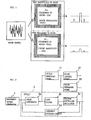
- Fig. 1 is a schematic view to illustrate an outline of the noise detection device of the present invention.
- the noise detection device according to the present invention performs noise detection by using the output from a PLL that is provided on a printed circuit board.
- a PLL which is provided as a circuit constituent element on the printed circuit board, can be used or can be provided especially for noise detection.
- the PLL is affected by noise from a noise source and, therefore, the signal strength, frequency, cycle, and signal waveform change.
- the noise detection device of the present invention performs noise detection on the basis of the signal in each part that constitutes the PLL.
- the noise detection device of the present invention detects how noise has an effect on an actually operating system by detecting how the noise has an effect on the PLL.
- PLLs are arranged in parts that are susceptible to noise and parts that are resistant to noise on the same printed circuit board and the effect of noise on these parts is detected on the basis of the output from the PLLs.
- a PLL with low noise tolerance and high noise sensitivity is provided in those parts which are susceptible to noise, while a PLL with high tolerance to noise and low noise sensitivity is provided in those parts which are resistant to noise.
- noise detection is executed from the output of the PLL provided in those parts susceptible to noise, but noise detection is not performed from the output of the PLL that is provided in those parts resistant to noise.
- noise detection that distinguishes between parts that are susceptible to noise and parts that are resistant to noise on the same printed circuit board cannot be implemented and, even when a plurality of noise detectors are arranged on the printed circuit board, the noise detectors have the same detection sensitivity and are therefore unable to detect noise by distinguishing between parts that are susceptible to noise and parts that are resistant to noise.
- noise detection device of the present invention noise detection according to noise tolerance can be executed on the same printed circuit board.
- the PLL it is possible to detect not only a noise level but also frequency, cycle, and so forth which serve as factors to determine whether the system actually malfunction or not.
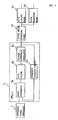
- Fig. 2 shows a first embodiment of the noise detection device of the present invention.
- noise detection is performed by using the output of the phase comparator that the PLL comprises.
- the noise detection device comprises a reference signal generator 1 that generates a reference signal, a PLL 2, and output measuring means (first measuring means) 11 that measure the output of the PLL 2.
- the PLL 2 comprises a voltage controlled oscillator 2c that controls the output frequency by means of an input voltage and a phase comparator that compares the phase of a signal that is outputted from the voltage controlled oscillator 2c with the phase of the reference signal, and a signal that is in synchronization with the reference signal is outputted by the voltage controlled oscillator 2c.
- the output of the phase comparator 2a with high frequency component thereof being removed by means of a loop filter 2b, becomes input voltage to the voltage controlled oscillator 2c.
- the output of the voltage controlled oscillator 2c may be frequency-divided at a predetermined ratio by means of a frequency division circuit 2d and then inputted to the phase comparator 2a. The provision of this frequency division circuit 2d makes it possible to form a frequency signal having a higher frequency than that of the reference signal.
- the output measuring means (first measuring means) 11 measure the output from the phase comparator 2a of the PLL 2.
- the phase comparator 2a compares the signal from the voltage controlled oscillator 2c or from frequency division circuit 2d with the reference signal and outputs a pulse-shaped phase difference signal.
- the loop filter 2b consists of an integration circuit and a lowpass filter, for example, and performs a DC current conversion by blocking the high frequency component of the phase difference signal.
- the voltage controlled oscillator 2c adjusts the oscillation frequency on the basis of the inputted control voltage and performs a phase adjustment operation in conjunction with the reference signal.
- the voltage controlled oscillator 2c is controlled such that the difference from the phase of the reference signal becomes zero by lowering the oscillation frequency to delay the phase in case where the signal phase of the output from the voltage controlled oscillator is advanced, or by raising the oscillation frequency to advance the phase in case where the signal phase is delayed.
- the phase comparator 2a outputs a signal that is based on the phase difference between the reference signal and the output of the voltage controlled oscillator 2c. This phase difference reflects the effect of noise on the PLL 2. In addition to the characteristics of the noise itself such as the wave height value of the noise and the frequency component thereof, the phase difference reflects the tolerance of the PLL 2 to noise.
- the output measuring means (first measuring means) 11 receives the output of the phase comparator 2a as a noise detection signal.
- noise judging means 21 and noise measuring means 22 can be connected to the output measuring means (first measuring means) 11.
- the noise judging means 21 judges the existence of noise on the basis of the output of the output measuring means (first measuring means) 11. This judgment can be performed by means of a comparison with a preset threshold value, for example.
- the noise measuring means 22 measures the scale of the noise on the basis of the output of the output measuring means (first measuring means) 11.
- the scale of the noise indicates an element such as a shift in the frequency of the noise or cycle shifts, or the like, in the PLL 2.
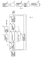
- Fig. 3 illustrates a second embodiment of the noise detection device of the present invention.
- noise detection is performed by using the output of the loop filter that the PLL comprises.
- the output of the loop filter is a signal that is based on the phase difference and, therefore, as shown in Fig. 3, the configuration of the noise detection device of this embodiment is substantially the same as that of the first embodiment shown in Fig. 2, but the output measuring means (second measuring means) 11 differs in that the output of the loop filter 2b is measured.
- the output measuring means (second measuring means) 11 differs in that the output of the loop filter 2b is measured.
- a description of the configuration that is common to that of the first embodiment will be omitted.
- the loop filter 2b removed the high frequency component from the output of the phase comparator 2a and then retrieves the DC component that is proportional to the phase difference.
- the output of the loop filter 2b reflects the effect of noise on the PLL and, other than the characteristics of the noise itself, such as the wave height value of the noise and the frequency component thereof, the output reflects the tolerance of the PLL to noise and, therefore, the level of risk that the system can actually be caused to malfunction can be judged by using the output of the loop filter 2b.
- Fig. 4 illustrates a third embodiment of the noise detection device of the present invention.
- noise detection is performed by using the output of a PLL to measure the amount of jitter.
- the configuration of the noise detection device is substantially the same as that of the first embodiment shown in Fig. 2 but differs in the fact that the output of the voltage controlled oscillator 2c is measured by means of the jitter amount measuring means 12, which constitute third measuring means.
- the jitter amount measuring means 12 which constitute third measuring means.
- the voltage controlled oscillator 2c controls the frequency by means of the voltage and changes the output frequency according to the voltage based on the phase difference that is obtained by the means of the phase comparator 2a and the loop filter 2b.
- This output frequency fluctuates to compensate for the shift in the frequency, cycle, or the like that is generated as a result of the effect of noise and the amount of jitter expresses the scale of the noise that exerts influence on the PLL 2.
- noise is detected by measuring the amount of jitter.
- the amount of jitter reflects the tolerance of the PLL to noise in addition to the characteristics of the noise itself such as the wave height value of the noise and the frequency component thereof, and so forth, and makes it possible to judge the level of risk that the system can actually be caused to malfunction.
- Figs. 5 to 7 signals that are measured by the respective measuring means (the first to third measuring means) for the noise that has occurred in the respective parts of the PLL will be described by using Figs. 5 to 7. Further, the signal example shown in Figs. 5 to 7 is shown in a simplified form. Further, each of these figures shows the reference signal and the difference in output caused by the scale of the noise with respect to the output of the voltage controlled oscillator, the output of the phase comparator, and the output of the loop filter. Figs. 5 to 7 show examples in which the scale of the noise is expressed as a phase difference and represent cases where (a) the phase delay of the output of the voltage controlled oscillator is large with respect to the reference signal, (b) the phase delay is small, and (c) a phase lead exists.
- the noise component is DC-converted by means of the loop filter and the frequency (cycle) of the voltage controlled oscillator is adjusted.
- (a) and (b) in Fig. 5 represent a case where a phase delay is generated by the noise.
- the phase comparator compares the output of the voltage controlled oscillator (phase delay) with a reference signal and outputs the comparison result as a phase difference signal and the loop filter DC-converts the phase difference corresponding to the phase delay.
- the voltage controlled oscillator adjusts the frequency (cycle) on the basis of the phase difference signal and thus matches the frequency to that of the reference signal.
- phase difference amount of the phase difference signal of the phase comparator and the wave-height value of the output of the loop filter vary according to the scale of the noise.
- (a) and (b) in Fig. 5 represent states where the phase delay of the output of the voltage controlled oscillator is small and large, respectively, according to the scale of the noise.
- (c) in Fig. 5 represents a state where the output of the voltage controlled oscillator is expressed as a phase lead in accordance with the scale of the noise.
- phase difference (comparator frequency (cycle)) of the voltage controlled oscillator varies according to the scale of the noise. In Fig. 5, this is expressed as the change in the interval (length of arrow) between the output signals of the voltage controlled oscillator.
- the noise component adjusts the frequency (cycle) of the voltage controlled oscillator.
- (a) and (b) in Fig. 6 represent cases where a phase delay is generated as a result of noise.
- the phase comparator compares the phase lag of the output of the voltage controlled oscillator with the reference signal and outputs the comparison result as a phase different signal, and the loop filter DC-converts the phase difference corresponding to the phase lag.
- the voltage controlled oscillator adjusts the frequency (cycle) on the basis of the phase comparison signal to match the reference signal.
- phase difference amount of the phase difference signal of the phase comparator and the wave height value of the output of the loop filter vary according to the scale of the noise.
- (a) and (b) in Fig. 6 represent states where the phase delay of the output of the voltage controlled oscillator is small and large, respectively, according to the scale of the noise.
- (c) in Fig. 5 represents a state where the output of the voltage controlled oscillator is expressed as a phase lead in accordance with the scale of the noise.
- phase difference (comparator frequency (cycle)) of the output of the voltage controlled oscillator varies according to the scale of the noise.
- this phase difference is expressed as the change in the interval between the output signals of the voltage controlled oscillator (length of the arrow).
- the noise component is compared with the reference signal by means of the phase comparator and outputted as a phase difference signal, and the loop filter DC-converts the phase difference.
- the voltage controlled oscillator adjusts the frequency (cycle) on the basis of the phase comparison signal to match the reference signal.
- phase difference amount of the phase difference signal of the phase comparator and the wave height value of the output of the loop filter vary according to the scale of the noise.
- (a) and (b) in Fig. 7 represent states where the phase lag of the output of the voltage controlled oscillator is small and large, respectively, according to the scale of the noise.
- (c) in Fig. 7 represents a state where the output of the voltage controlled oscillator is expressed as a phase lead in accordance with the scale of the noise.
- phase difference (comparator frequency (cycle) ) of the output of the voltage controlled oscillator varies according to the scale of the noise. In Fig. 7, this is expressed as the change in the interval (length of the arrow) between the output signals of the voltage controlled oscillator.
- the respective measuring means (first measuring means to third measuring means) of the noise detection device of the present invention perform noise detection on the basis of the output of the phase comparator, the output of the loop filter, and the output of the voltage controlled oscillator.
- the judgment result of the noise judging means 21 and the measurement result of the noise measuring means 22 can be stored by the storage means 32 in addition to being displayed by the screen display means 31 as shown in Figs. 8 and 9. Further, Figs. 8 and 9 only show the noise judging means 21, where illustration of the noise measuring means 22 is omitted.
- the noise detection device of the present invention is able to change the noise sensitivity of the PLL.
- the noise sensitivity of the PLL can be changed by changing the characteristic of the loop filter, for example.
- the noise sensitivity of the PLL can also be changed by changing the characteristics of the voltage controlled oscillator and the characteristics of the power supply.
- the noise sensitivity of the loop filter can be changed by changing the integration constant by changing the condenser and resistance components, for example.
- the noise sensitivity of PLL can be changed by providing a plurality of loop filters (loop filter 1 and loop filter 2) with different noise sensitivities in the PLL 2 and selecting any one of them by means of switching means 2e.
- Fig. 11 is an example of a configuration that measures the position in which noise occurs and the noise distribution.
- a plurality of noise detection devices comprising reference signal generators 1A to 1N, PLL 2A to 2N, measuring means 10A to 10N, and noise judging means 21A to 21N are provided on a printed circuit board or in each part of an electronic device and the noise judgment result obtained by the noise detection device is inputted to position judging means 33 to determine the position in which the noise occurred and the noise distribution.
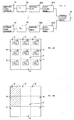
- Fig. 12A shows an example in which a plurality of PLLs are arranged on the same printed circuit board to measure a noise generation distribution.
- the placement example shown in Fig. 12A shows an example in which the printed circuit board is divided up into nine regions, namely, A, B, ..., I, and PLL 2A, 2B, ..., 2I are arranged in each region.
- a noise detection signal is detected from the PLL 2A and PLL 2B that are arranged in each region.
- the screen display means 31 are able to display the noise distribution on the basis of these noise detection signals.
- Fig. 12B is an example of a noise distribution display.
- the configuration can also be one in which the noise distribution is found in combination with alarm production.
- Fig. 13 shows an outline of an example of a configuration in which noise distribution at the time of alarm occurrence is measured.
- N noise detection devices with the above configuration that includes the reference signal generators 1A to 1N and PLLs 2A to 2N comprises the respective storage means (storage and reading means) 32A to 32N.
- the respective storage means 32A to 32N are constituted by a register and a buffer, and so forth, and store the outputs from the PLL 2A to 2N.
- the storage means 32A to 32N are able to store past output data from the PLL 2A to 2N within a predetermined time interval from the current time by sequentially updating the output data of a predetermined recording capacity at all times.
- the time interval for the storage depends on the recording capacity of the storage means 32A to 32N and, therefore, the recording capacity of the storage means 32A to 32N is set according to the required time interval.
- the outputs of the PLL 2A to 2N stored by the storage means 32A to 32N can be the output of the phase comparator 2a, the output of the loop filter 2b, and the output of the voltage controlled oscillator 2c, and so forth, as shown in each of the embodiments above.
- the configuration example shown in Fig. 13 is one in which the output of the phase comparator 2a is stored, the output of the loop filter 2b or the output of the voltage controlled oscillator 2c can also be stored, or an optional output can also be stored in accordance with the configuration of the PLL and the dispositional position of the PLL and so forth.
- the PLL output data stored by the storage means 32A to 32N is read out to noise distribution creation means 35 according to an input of an alarm signal.
- the noise distribution creation means 35 create a noise distribution on the basis of output data that is read out from the respective storage means 32 and displays the noise distribution on the screen display means 31.
- the position judging means 33 comprise a function to create a noise distribution from the mount position of each PLL, and are able to acquire the position of the PLL to create the noise distribution, by acquiring data on the installation position of each PLL that has been provided in advance or by acquiring data on the installation position from each PLL.
- noise distribution creation in addition to creating a distribution at the time of noise occurrence by using noise data at the time of alarm generation, the noise distribution of a predetermined time interval until the noise occurs can also be created by using noise data within a predetermined time interval starting with generation of noise.
- Fig. 14 is an example in which a combination of alarm production and noise data storage/display is implemented.
- the output of the storage means (noise data storage means) 32 and the alarm signal are inputted to alarm judging means 34.
- Alarm judging means 34 judge whether the alarm is attributable to noise by using noise data at the time when the alarm signal is inputted and display the judgment result on the screen display means (noise data screen display means) 31.
- Fig. 15A is an example of a noise distribution.
- a PLL that is constituted to enable the noise sensitivity to be changed as per the configuration shown in Fig. 10 is arranged in each region of the printed circuit board.
- Fig. 10 shows an example in which the noise sensitivity is set in three stages, namely low sensitivity, medium sensitivity and high sensitivity.
- the noise source is in a position above and to the right of center of the printed circuit board
- the noise sensitivity when the noise sensitivity is set low, only the PLL in the center region detects noise and the noise distribution shown in Fig. 15B is obtained.
- the noise sensitivity when the noise sensitivity is set to medium, the PLLs in the center region and in the center right-hand region detect noise, for example, and the noise distribution shown in Fig. 15C is obtained.
- the noise sensitivity is set to high, the PLLs in the top center region, right-hand region, center region, center right-hand region and lower right-hand region detect noise, for example, and the noise distribution shown in Fig. 15D is obtained.
- the noise detection device of the present invention is able to detect noise that is fatal to the system through the use of a PLL that is the most susceptible to noise in the system. Further, the PLL is contained in virtually all the ASICs used by the system and a noise detection circuit can be implemented by means of simple circuit addition. Therefore, noise detection is possible at a large number of points in the system without an increase in costs.
- the noise detection device of the present invention can be applied to a variety of electronic devices, electric devices, and so forth and, more particularly, in the case of an electronic device that contains a circuit that uses a plurality of clock signals, because a PLL is used for the formation of the clock signal, the PLL that the circuit itself comprises can be used.
Landscapes
- Physics & Mathematics (AREA)
- General Physics & Mathematics (AREA)
- Stabilization Of Oscillater, Synchronisation, Frequency Synthesizers (AREA)
- Measurement Of Current Or Voltage (AREA)
- Measurement Of Velocity Or Position Using Acoustic Or Ultrasonic Waves (AREA)
Applications Claiming Priority (2)
| Application Number | Priority Date | Filing Date | Title |
|---|---|---|---|
| JP2004013234 | 2004-01-21 | ||
| JP2004013234A JP4070725B2 (ja) | 2004-01-21 | 2004-01-21 | ノイズ検出機能を備える電子機器 |
Publications (2)
| Publication Number | Publication Date |
|---|---|
| EP1557681A2 true EP1557681A2 (fr) | 2005-07-27 |
| EP1557681A3 EP1557681A3 (fr) | 2005-10-19 |
Family
ID=34631909
Family Applications (1)
| Application Number | Title | Priority Date | Filing Date |
|---|---|---|---|
| EP05250278A Ceased EP1557681A3 (fr) | 2004-01-21 | 2005-01-20 | Appareil de détection de bruit |
Country Status (4)
| Country | Link |
|---|---|
| US (1) | US7519113B2 (fr) |
| EP (1) | EP1557681A3 (fr) |
| JP (1) | JP4070725B2 (fr) |
| CN (1) | CN100392413C (fr) |
Families Citing this family (19)
| Publication number | Priority date | Publication date | Assignee | Title |
|---|---|---|---|---|
| US8736323B2 (en) * | 2007-01-11 | 2014-05-27 | International Business Machines Corporation | Method and apparatus for on-chip phase error measurement to determine jitter in phase-locked loops |
| US7881608B2 (en) * | 2007-05-10 | 2011-02-01 | Avago Technologies Fiber Ip (Singapore) Pte. Ltd | Methods and apparatuses for measuring jitter in a transceiver module |
| DE112007003552T5 (de) | 2007-06-20 | 2010-06-10 | Advantest Corporation | Störungsmessgerät und Prüfgerät |
| JP5112250B2 (ja) * | 2008-10-16 | 2013-01-09 | 矢崎総業株式会社 | 基板の冷却器及び高周波信号の測定器 |
| US20100109787A1 (en) * | 2008-10-31 | 2010-05-06 | Alcatel Lucent | Method and apparatus for oscillator stability verification |
| TW201106645A (en) * | 2009-08-14 | 2011-02-16 | Ralink Technology Corp | Method for detecting continuous channel noise and apparatus for using the same |
| FR2963180B1 (fr) * | 2010-07-26 | 2012-08-10 | Sagem Defense Securite | Systeme de reference de frequence non affecte de micro-sauts de frequence |
| US8977222B2 (en) * | 2012-11-19 | 2015-03-10 | Broadcom Corporation | Phase-noise reduction technique using frequency-to-current conversion with baseband integration |
| JP6077290B2 (ja) * | 2012-12-06 | 2017-02-08 | ルネサスエレクトロニクス株式会社 | 半導体装置、無線通信端末及び半導体装置の制御方法 |
| CN104865877B (zh) * | 2015-06-05 | 2018-01-02 | 京东方科技集团股份有限公司 | 一种电子设备 |
| US9743206B2 (en) * | 2015-06-22 | 2017-08-22 | Audyssey Laboratories, Inc. | Background noise measurement from a repeated stimulus measurement system |
| JP6444851B2 (ja) * | 2015-12-24 | 2018-12-26 | ファナック株式会社 | ノイズの発生原因を検出する学習機能を有する制御装置 |
| CN106775142B (zh) * | 2015-12-31 | 2019-10-01 | 深圳市汇顶科技股份有限公司 | 电容感测电路 |
| US10148272B2 (en) * | 2017-05-03 | 2018-12-04 | Ping-Ying Wang | Frequency generating circuit using quartz crystal resonator |
| CN106990367B (zh) * | 2017-05-22 | 2019-08-06 | 中国电子产品可靠性与环境试验研究所 | SoC片上电源噪声监测系统 |
| US11181396B2 (en) * | 2018-04-10 | 2021-11-23 | Hemy8 Sa | Noise-resistant intermittently operating incremental position sensor |
| CN110335447A (zh) * | 2019-07-26 | 2019-10-15 | 广东中检检测技术有限公司 | 一种室内噪音监控报警系统 |
| CN113701874A (zh) * | 2021-07-14 | 2021-11-26 | 福建九五检测技术服务有限公司 | 一种带有安装结构的噪声检测装置及其检测方法 |
| TWI908634B (zh) * | 2025-03-17 | 2025-12-11 | 英業達股份有限公司 | 噪音檢測方法 |
Citations (2)
| Publication number | Priority date | Publication date | Assignee | Title |
|---|---|---|---|---|
| US20010006343A1 (en) * | 1999-11-30 | 2001-07-05 | Akihiko Yoshizawa | Integrated circuit and lot selection system therefor |
| JP2003142586A (ja) * | 2001-10-31 | 2003-05-16 | Seiko Epson Corp | ノイズ検出装置および半導体集積回路 |
Family Cites Families (12)
| Publication number | Priority date | Publication date | Assignee | Title |
|---|---|---|---|---|
| CN85202661U (zh) * | 1985-07-04 | 1986-04-23 | 清华大学 | 高速低相噪锁相环式频率合成器 |
| JPH01307316A (ja) | 1988-06-06 | 1989-12-12 | Nec Corp | 位相同期発振器 |
| JPH06164380A (ja) | 1992-06-05 | 1994-06-10 | Nec Corp | 位相同期検出回路 |
| DE4417115C1 (de) | 1994-05-16 | 1996-03-14 | Inst Rundfunktechnik Gmbh | Schaltungsanordnung zur Messung des Jitters in einem System, das serielle Daten hoher Bitrate, insbesondere digitale Fernsehsignale über ein Koaxialkabel überträgt |
| CN1065397C (zh) * | 1998-08-05 | 2001-05-02 | 国家科学技术委员会高技术研究发展中心 | 低相位噪声调谐器及其实现方法 |
| JP4087976B2 (ja) | 1999-03-12 | 2008-05-21 | 株式会社エー・アンド・デイ | 電気的外乱ノイズを検出する電子秤 |
| US6476396B1 (en) * | 1999-04-09 | 2002-11-05 | Keith W. Forsyth | Electro-optical, non-contact measurement of electrical discharges |
| JP2001274679A (ja) | 2000-03-24 | 2001-10-05 | Mitsubishi Electric Corp | Pll回路 |
| US6356158B1 (en) * | 2000-05-02 | 2002-03-12 | Xilinx, Inc. | Phase-locked loop employing programmable tapped-delay-line oscillator |
| JP2003287555A (ja) * | 2002-03-28 | 2003-10-10 | Advantest Corp | 位相雑音測定方法及びその方法を用いた位相雑音測定装置 |
| JP2003332442A (ja) | 2002-05-08 | 2003-11-21 | Nec Corp | ノイズ検出方法と該ノイズ検出方法による基板 |
| KR100510487B1 (ko) * | 2002-05-28 | 2005-08-26 | 삼성전자주식회사 | 넓은 동기 범위를 갖는 위상동기루프 회로 및 이를 구비한반도체 집적회로 장치 |
-
2004
- 2004-01-21 JP JP2004013234A patent/JP4070725B2/ja not_active Expired - Fee Related
-
2005
- 2005-01-19 US US11/037,003 patent/US7519113B2/en not_active Expired - Fee Related
- 2005-01-20 EP EP05250278A patent/EP1557681A3/fr not_active Ceased
- 2005-01-21 CN CNB2005100026002A patent/CN100392413C/zh not_active Expired - Fee Related
Patent Citations (2)
| Publication number | Priority date | Publication date | Assignee | Title |
|---|---|---|---|---|
| US20010006343A1 (en) * | 1999-11-30 | 2001-07-05 | Akihiko Yoshizawa | Integrated circuit and lot selection system therefor |
| JP2003142586A (ja) * | 2001-10-31 | 2003-05-16 | Seiko Epson Corp | ノイズ検出装置および半導体集積回路 |
Also Published As
| Publication number | Publication date |
|---|---|
| EP1557681A3 (fr) | 2005-10-19 |
| CN100392413C (zh) | 2008-06-04 |
| US20050157829A1 (en) | 2005-07-21 |
| CN1645154A (zh) | 2005-07-27 |
| JP4070725B2 (ja) | 2008-04-02 |
| US7519113B2 (en) | 2009-04-14 |
| JP2005210297A (ja) | 2005-08-04 |
Similar Documents
| Publication | Publication Date | Title |
|---|---|---|
| US7519113B2 (en) | Noise detection device | |
| KR100721349B1 (ko) | 확산 스펙트럼 클록 생성기를 제어하기 위한 방법 및 확산 스펙트럼 클록 생성 회로 | |
| US6522122B2 (en) | Jitter measuring device and method | |
| US8736323B2 (en) | Method and apparatus for on-chip phase error measurement to determine jitter in phase-locked loops | |
| US6819153B2 (en) | Semiconductor device for clock signals synchronization accuracy | |
| US6768385B2 (en) | Intelligent phase lock loop | |
| US6664830B2 (en) | Low pass filters in DLL circuits | |
| US6832173B1 (en) | Testing circuit and method for phase-locked loop | |
| US7375592B2 (en) | System and method for maintaining an accurate frequency on a voltage controlled oscillator | |
| EP1024367B1 (fr) | Circuit de test à mesure de fréquence et circuit integré semi-conducteur le comprenant | |
| US6304119B1 (en) | Timing generating apparatus with self-calibrating capability | |
| US7705581B2 (en) | Electronic device and method for on chip jitter measurement | |
| US20110285419A1 (en) | Semiconductor integrated circuit for generating clock signals | |
| US6342849B1 (en) | Method and apparatus for peak detection of an analog signal | |
| KR101201116B1 (ko) | 동적 루프 대역을 갖는 위상고정루프 및 동적 루프 대역을 사용하여 기준신호에 동기하는 출력신호를 생성하는 방법 | |
| JP3647699B2 (ja) | 集積回路及びロット選別システム | |
| US6693845B2 (en) | Semiconductor device having PLL-circuit | |
| JP4979003B2 (ja) | Cdr回路 | |
| US20250330182A1 (en) | Shock recovery | |
| JPH05264753A (ja) | 遅延時間測定装置 | |
| KR20010008838A (ko) | 디지탈 클럭 동기 시스템에서 이중 위상 제어를 이용한 클럭동기 장치 및 방법 | |
| WO2008152082A1 (fr) | Dispositif électronique et procédé de mesure de la gigue sur la puce | |
| KR20060090026A (ko) | 지연동기루프에서의 디지탈 락 검출장치 및 검출방법 |
Legal Events
| Date | Code | Title | Description |
|---|---|---|---|
| PUAI | Public reference made under article 153(3) epc to a published international application that has entered the european phase |
Free format text: ORIGINAL CODE: 0009012 |
|
| AK | Designated contracting states |
Kind code of ref document: A2 Designated state(s): AT BE BG CH CY CZ DE DK EE ES FI FR GB GR HU IE IS IT LI LT LU MC NL PL PT RO SE SI SK TR |
|
| AX | Request for extension of the european patent |
Extension state: AL BA HR LV MK YU |
|
| PUAL | Search report despatched |
Free format text: ORIGINAL CODE: 0009013 |
|
| AK | Designated contracting states |
Kind code of ref document: A3 Designated state(s): AT BE BG CH CY CZ DE DK EE ES FI FR GB GR HU IE IS IT LI LT LU MC NL PL PT RO SE SI SK TR |
|
| AX | Request for extension of the european patent |
Extension state: AL BA HR LV MK YU |
|
| RIC1 | Information provided on ipc code assigned before grant |
Ipc: 7G 01R 29/26 B Ipc: 7G 01R 23/20 A |
|
| 17P | Request for examination filed |
Effective date: 20060201 |
|
| AKX | Designation fees paid |
Designated state(s): DE |
|
| 17Q | First examination report despatched |
Effective date: 20061113 |
|
| RAP1 | Party data changed (applicant data changed or rights of an application transferred) |
Owner name: FANUC CORPORATION |
|
| STAA | Information on the status of an ep patent application or granted ep patent |
Free format text: STATUS: THE APPLICATION HAS BEEN REFUSED |
|
| 18R | Application refused |
Effective date: 20111201 |