EP1555688A2 - Ein FinFET mit mehrseitigem Kanal und zugehöriges Herstellungsverfahren. - Google Patents
Ein FinFET mit mehrseitigem Kanal und zugehöriges Herstellungsverfahren. Download PDFInfo
- Publication number
- EP1555688A2 EP1555688A2 EP05000303A EP05000303A EP1555688A2 EP 1555688 A2 EP1555688 A2 EP 1555688A2 EP 05000303 A EP05000303 A EP 05000303A EP 05000303 A EP05000303 A EP 05000303A EP 1555688 A2 EP1555688 A2 EP 1555688A2
- Authority
- EP
- European Patent Office
- Prior art keywords
- fin
- channel
- base
- finfet
- semiconductor
- Prior art date
- Legal status (The legal status is an assumption and is not a legal conclusion. Google has not performed a legal analysis and makes no representation as to the accuracy of the status listed.)
- Granted
Links
Images


Classifications
-
- H—ELECTRICITY
- H10—SEMICONDUCTOR DEVICES; ELECTRIC SOLID-STATE DEVICES NOT OTHERWISE PROVIDED FOR
- H10P—GENERIC PROCESSES OR APPARATUS FOR THE MANUFACTURE OR TREATMENT OF DEVICES COVERED BY CLASS H10
- H10P10/00—Bonding of wafers, substrates or parts of devices
-
- H—ELECTRICITY
- H10—SEMICONDUCTOR DEVICES; ELECTRIC SOLID-STATE DEVICES NOT OTHERWISE PROVIDED FOR
- H10D—INORGANIC ELECTRIC SEMICONDUCTOR DEVICES
- H10D30/00—Field-effect transistors [FET]
- H10D30/01—Manufacture or treatment
- H10D30/021—Manufacture or treatment of FETs having insulated gates [IGFET]
- H10D30/024—Manufacture or treatment of FETs having insulated gates [IGFET] of fin field-effect transistors [FinFET]
-
- H—ELECTRICITY
- H10—SEMICONDUCTOR DEVICES; ELECTRIC SOLID-STATE DEVICES NOT OTHERWISE PROVIDED FOR
- H10D—INORGANIC ELECTRIC SEMICONDUCTOR DEVICES
- H10D30/00—Field-effect transistors [FET]
- H10D30/60—Insulated-gate field-effect transistors [IGFET]
- H10D30/62—Fin field-effect transistors [FinFET]
- H10D30/6212—Fin field-effect transistors [FinFET] having fin-shaped semiconductor bodies having non-rectangular cross-sections
- H10D30/6213—Fin field-effect transistors [FinFET] having fin-shaped semiconductor bodies having non-rectangular cross-sections having rounded corners
Definitions
- the invention relates to a multi-sided-channel FinFET transistor according to the preamble of claim 1, and to a method of forming such transistor.
- FIGs. 5A-5B are side views that depict stages of the peculiar form of locomotion used by an inchworm 602.
- a head 604 and a tail 606 of inchworm 602 are close together while a middle section 608 thereof is hunched upward (or, in other words, folded almost in half).
- inchworm 602 has moved its head 604 forward while keeping its tail 606 in the same position as in Fig. 5A, which causes middle section 608 to be stretched horizontally relative to Fig. 5A.
- Fig. 5A-5B are side views that depict stages of the peculiar form of locomotion used by an inchworm 602.
- a head 604 and a tail 606 of inchworm 602 are close together while a middle section 608 thereof is hunched upward (or, in other words, folded almost in half).
- inchworm 602 has moved its head 604 forward while keeping its tail 606 in the same position as in Fig. 5A, which causes middle section 608 to be stretched horizontally relative to Fig. 5A.
- inchworm 602 has kept its head 604 in the same position as in Fig. 5B, but has moved its tail 606 to again be located near its head 604. As such, inchworm 602 has adopted in Fig. 5C the same posture as in Fig. 5A.
- the larger footprint transistor architecture according to the Background Art is analogous to the posture of inchworm 602 in Fig. 5B, where the channel corresponds to the horizontally stretched middle section 608 of inchworm 602.
- the smaller footprint transistor architecture according to the Background Art is analogous to the posture of inchworm 602 in Figs. 5A and 5C, where the channel corresponds to the hunched-upward or folded middle section 608.
- Fig. 6 is a three-quarter perspective view of the smaller footprint architecture according to the Background Art, which is generally referred to as a FinFET and particularly here as a triple gate FinFET 700, i.e., FET having a channel in the shape of a fin 702b (obscured in Fig. 6 but see Fig. 7) formed on a buried oxide (BOX) structure 701 between a source region 702a and a drain region 702C.
- BOX buried oxide
- Gate electrode 706 conforms (as does interposed gate oxide layer 704) to the shape of channel 704
- Fig. 7 is a cross-sectional view of Background Art FinFET 700 taken along line VII-VII' of Fig. 6. Recall that the inversion layer induced in a channel is located next to gate oxide 704 and tends to be rather shallow.
- An idealized effect of the fin-shaped channel 704 gate electrode 706 is as if three separate inversion layers are induced, namely a first inversion layer 708a, a second inversion layer 708b and a third inversion layer 708C.
- FinFET 700 is referred to as a triple-gate FinFET.
- Figs. 8A-8B are cross-sectional views of two stages in the manufacture of a multi-gate FinFET according to the Background Art. More particularly, Figs. 8A-8B depict stages in the formation of the fin of the FinFET.
- a silicon layer 220 is formed on a buried oxide (BOX) structure 210, which is formed on a silicon substrate 220.
- a silicon plug 810 is formed to fill an opening in oxide layer 510. Plug 810 is grown by selective epitaxial growth (SEG).
- SEG selective epitaxial growth
- the portion of plug 810 extending above oxide 510 has been removed by CMP.
- the electrostatic field induced by a voltage on gate electrode, e.g., 706, is not uniform along gate electrode 706. Rather, the electrostatic field tends to be concentrated in the corners, as indicated by the shaded regions 710a and 710b in Fig. 7. Consequently, inversion layers form in the corners before forming all along gate electrode 706. This lowers a threshold voltage for the corners relative to the sides, leading to higher current flow at the corners and generally non-uniform performance of the FinFET.
- the Background Art recognized that such a corner phenomenon could be mitigated if the corners could be rounded. Accordingly, efforts have been made to remove material from the substantially square corners, e.g., by dry etching, in order to achieve an approximation of rounded corners. Despite many attempts, the Background Art has not been able to develop a technique to remove material from square corners of triple-gate FinFET 700 (or a double-gate version thereof) that does not irreparably damage the remaining portion of fin 702b or result in a non-uniform width thereof.
- the invention solves this problem by providing a multi-sided-channel FinFET transistor having the features of claim 1 and a method of forming an at least penta-sided-channel type of FinFET transistor having the features of claim 13.
- At least one embodiment of the invention provides an at least penta-sided-channel type of FinFET transistor.
- a FinFET may include: a base; a semiconductor body formed on the base, the body being arranged in a long dimension to have source/drain regions sandwiching a channel region, where at least the channel, in cross-section transverse to the long dimension, has at least five planar surfaces above the base; a gate insulator on the channel region of the body; and a gate electrode formed on the gate insulator.
- At least one embodiment of the invention provides a method of forming an at least penta-sided-channel type of FinFET transistor.
- Such a method may include: providing a base; forming a fin on the base; epitaxially growing a body of semiconductor material, which includes a channel region, on the base, where at least the channel region, in cross-section transverse to a long dimension of the body, having five or more planar surfaces above the base; selectively doping the semiconductor body to produce, in the long dimension, source/drain regions sandwiching the channel region, forming a gate insulator on the channel region of the body; and forming a gate electrode formed on the gate insulator.
- Fig. 1 is a three-quarter perspective view of an at least penta-sided-channel type of FinFET transistor, according to an embodiment of the invention.
- Fig. 2A is a cross-sectional view (taken along line II-II' of Fig. 1) of a first variety 1a of FinFET transistor 1, according to an embodiment of the invention.
- Figs. 2B-2E are cross-sectional views (also taken along line II-II' of Fig. 1) of other varieties 1X (where X ⁇ B,C,D,E ⁇ ) of FinFET transistor 1, according to embodiments of the invention, respectively.
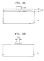
- Figs. 3A -3H are cross-sectional views (from the same perspective of Fig. 2B) that depict various stages of a method, according to an embodiment of the invention, of making the FinFET of Fig. 2B.
- Figs. 4A -4C are cross-sectional views (from the same perspective of Fig. 2E) that depict various stages of a method, according to an embodiment of the invention, of making the FinFET of Fig. 2E.
- Figs. 5A-5C are side views that depict stages of the peculiar form of locomotion used by an inchworm, which are presented as background information for an analogy to a FinFET according to the Background Art.
- Fig. 6 is a three-quarter perspective view of a FinFET according to the Background Art.
- Fig. 7 is a cross-sectional view of the Background Art FinFET of Fig. 6, taken along line VII-VII'.
- Figs. 8A-8B are cross-sectional views of two stages in the manufacture of a multi-gate FinFET, according to the Background Art.
- the Background Art assumes that mitigation (by rounded-corner approximation) of the problematic corner effect (again, caused by substantially square corners of the fin-shaped channel) of a Background Art FinFET can only be accomplished subtractively by removing material representing the substantially square portion of the corners. It is now recognized that an obtuse angle significantly larger than 90° can significantly reduce the corner effect. Such an obtuse angle approximates the rounding of corners, but can be achieved additively by growing the fin rather than subtractively by removing material from a fin having substantially square corners.
- An embodiment of the invention provides a multiple sided channel FinFET having approximated rounded comers for the fin-shaped body (in which the channel is induced) by additively constructing, e.g., growing, a body of semiconductor material into the desired shape.
- Fig. 1 is a three-quarter perspective view of an at least penta-sided-channel type of FinFET transistor 1, according to an embodiment of the invention.
- Fig. 2A is a cross-sectional view (taken along line II-II' of Fig. 1) of a first variety 1a of at least the penta-sided-channel-type FinFET transistor 1, according to an embodiment of the invention.
- Figs. 2B-2E are cross-sectional views (also taken along line II-II' of Fig. 1) of other varieties 1X (where X ⁇ B,C,D,E) ⁇ of FinFET transistor 1, according to other embodiments of the invention, respectively, that will be discussed below.
- Transistor 1 includes: a substrate 10; an isolation region 12; a fin 14 (obscured in Fig. 1, but see, e.g., Fig. 2A); a body 20 of semiconductor material, the body having two substantially vertical (relative to substantially horizontal isolation region 12) facets 22, a substantially horizontal facet 24, and two beveled (again, relative to isolation region 12) facets 26; a channel 28 (obscured in Fig. 1, but see, e.g., Fig. 2A); a gate insulating layer 40; source/drain regions 44; a gate electrode 50 having two instances of a first gate regions 50a, two instances of a second gate region 50b, and one instance of a third gate region 50c.
- a penta-sided inversion layer (or, in other words, a penta-sided channel) is induced in the mushroom-shaped portion 20a of body 20 of FinFET transistor 1a.
- channel 20a is depicted as being transverse to a long dimension of body 20, where body 20 also contains source/drain regions 44.
- Portion 20a of body 20 has a penta-sided head portion 27p (where the suffix "p" is suggestive of the prefix penta-) and a stalk portion 29A.
- Stalk portion 29A extends down into and fills a recess defined by sidewalls 12L and 12R of isolation region 12 and an upper surface 14u of fin 14.
- penta-sided head portion 27p exhibits five facets that can be described as being located above isolation region 12, namely: two instances of substantially vertical facet 22; one instance of substantially horizontal facet 24; and two instances of beveled facet 26.
- the five gate electrode regions 50a, 50b, 50c, 50b and 50a can induce five inversion regions in body 20a, which in effect represent five channels.
- Obtuse angles between facets 22 & 26 and 26 & 24 are substantially greater, respectively, than the 90° angles exhibited by the corners according to Background Art FinFET 700, hence the problems associated with the corner effect are at least substantially reduced.
- Substrate 10 can include, e.g., one or more of ⁇ 100 ⁇ bulk Si, Si, Ge, SiGe, GaP, GaAs, SiC, SiGeC, InAs, InP, etc.
- Semiconductor body 20 can include, e.g., one or more of Si, Ge, SiGe, SiC, SiGeC, etc. (discussed further below).
- Gate insulating layer 40 can include, e.g., one or more of SiO2, SiON, Si 3 N 4 , Ge x O y N z , Ge x Si y O z , high-k metal oxide (e.g., HfO 2 , ZrO 2 , Al 2 O 3 , TiO 2 , Ta 2 O 5 , etc.), etc. or a stacked structure thereof.
- gate 50 can include one or more of doped poly-Si, metal (e.g., Al, W, Pt, etc.), metal nitride (e.g., TiN) metal (e.g., Co, Ni, Ti, Hf, Pt) silicide alloy, etc. or a stacked structure thereof.
- Fig. 2B is a cross-sectional view (again, taken along line II-II' of Fig. 1) of a second variety 1b of at the at-least-penta-sided-channel-type FinFET transistor 1, according to another embodiment of the invention.
- FinFET 1b is similar to FinFET 1a, so minimal discussion of similarities is presented for the sake of brevity.
- stalk portion 29a of FinFET 1a is substantially rectangular in cross-section
- stalk 29b of FinFET 1b is tapered by contrast.
- Sidewall spacers 60 partially fill the recess defined by sidewalls of isolation region 12 and upper surface 14u of fin 14. However, a portion of upper surface 14u is not covered by sidewall spacers 60, but instead is covered by the smaller end of stalk portion 29A.
- the five facets of head portion 27p of FinFETs 1a and 1b are obtained by growing bodies 20a and 20b, e.g., via selective epitaxial growth (SEG). Faceting morphology of head portion 27p, in terms of Miller indices, can include: horizontal facet 24 exhibiting plane (100); and beveled facets 26 exhibiting plane (311) or (111). Together, the five facets define a silhouette in Fig. 2B (and Fig. 2A) that approximates a fin having substantially rounded comers, as contrasted with fin 702b according to the Background Art. In other words, above isolation region 12, head portion 27p has a polygonal silhouette having five or more sides.
- Figs. 3A -3H are cross-sectional views (from the same perspective of Fig. 2B) that depict various stages of a method, according to an embodiment of the invention, of making FinFET 1b.
- substrate 10 as been provided.
- An oxide layer 102 has been formed on substrate 10.
- a silicon nitride layer 104 has been formed on oxide layer 102.
- layers 102 and 104 define a mask layer 105.
- a photo-resist (PR) material has been deposited on mask layer 105 and patterned into PR pattern 106.
- PR photo-resist
- Figs. 3A and 3B depict what is depicted in Figs. 3A and 3B. Then PR pattern 106 is itself removed.
- Fig. 3B depicts what remains thereafter, namely a mask 105a formed of layer segments 104a and 102a.
- Fig. 3C portions of substrate 10 have been selectively removed, causing substrate 10 to take on an inverted-T shape having a horizontal portion and fin 14 extending perpendicularly therefrom. As a result, one or more trenches T have been formed above the horizontal portion of substrate 10 and around the sides of fin 14.
- isolation region 112 has been formed, e.g., by deposition of material to fill one or more trenches T. Also, optionally, isolation region 112 and mask 105a have been planarized. In Fig. 3E, mask 105a has been removed, e.g., by wet etching, leaving a recess 113 defined by the exposed sidewalls of isolation region 12 and an upper surface of fin 14.
- optional sidewall spacers 60 have been formed against the formerly exposed sidewalls of isolation region 12 and on portions of the upper surface of fin 14. This can be done by filling recess 113 with a nitride or oxide material and then partially removing the material. The remaining filler material 60 takes on the appearance of sidewall spacers.
- portion 20b (and thus body 20) of semiconductor material will be grown, e.g., via SEG.
- portion 20b (and thus body 20) has been grown, e.g., (again) via SEG, such that it has penta-sided head portion 27p (with facets 22, 24 and 26) and stalk portion 29b.
- ion implantation has been performed to obtain source/drain regions 44 (not shown in Fig. 3G, but see Fig. 1).
- CMOS processing occurs by which FinFET 1b is completed.
- a layer of insulating material has been formed on outer surfaces of penta-sided head portion 27p of portion 20b of body 20 that are located above isolation region 12 as well as on portions of the upper surface of isolation region 12.
- Those portions of the insulating material not contiguous with penta-sided head portion 27p have been selectively removed, which results in gate insulating layer 40.
- gate electrode layer 150 has then been formed on gate insulating layer 40 and on portions of the upper surface of isolation region 12. Accordingly, the stage of FinFET manufacture depicted in Fig. 3H corresponds to Fig. 2B.
- sidewall spacers 60 are optional. If sidewall spacers 60 are not formed (or, in other words, the stage depicted in Fig. 3F is omitted), then SEG can be performed on the intermediate structure of Fig. 3E, so that the subsequent processing associated with Figs. 3G and 3H would produce FinFET 1a instead of FinFET 1b.
- SEG-process parameters can be controlled to manipulate the growth of body 20a or 20b so that penta-sided head portion of 27p results, different measures are needed to control an overall size of body 20 (and thus a scale of FinFET 1a or 1b).
- the surface area of the seed upon which SEG takes place is proportional to the overall size of resulting body 20.
- the use of sidewall spacers 60 represents a technique to reduce an overall size that body 20 (and therefore FinFET 1b) can obtain. More particularly, the seed area of Fig. 3E is larger than the seed area of Fig. 3F, hence for similar SEG parameters, portion 20b of body 20 would be expected to be smaller than portion 20a of body 20.
- the SEG process can include the following.
- the exposed upper surface 14u of fin 14 is cleaned via, e.g., the RCA cleaning technique, which uses a mixture of H2SO 4 , HCl, NH 4 OH, HF and H 2 O 2 to remove native oxide from the seed.
- the SEG process can begin.
- temperatures can range between about 500°C to about 900 °C
- pressures can range between about 5 to about 100 Torr
- dichlorosilane (DCS) gas can be used as the atmosphere in which growth takes place.
- DCS dichlorosilane
- Fig. 2C is a cross-sectional view (again, taken along line II-II' of Fig. 1) of a third variety 1c of the at-least-penta-sided-channel-type FinFET transistor 1, according to another embodiment of the invention.
- FinFET 1c is similar to FinFET 1b, so minimal discussion of similarities is presented for the sake of brevity.
- portion 20b of body 20 of FinFET 1b is formed of substantially one material
- corresponding portion 20c of body 20 of FinFET 1c includes two materials, namely a mound 16 of strain-inducing semiconductor material and a layer 18 of strained semiconductor material.
- an advantage of strained semiconductor material e.g., silicon, is that it exhibits reduced resistance to electron/hole mobility.
- Mound 16 of strain-inducing material can be described as a smaller version of portion 20b of body 20. Gas components of the atmosphere provided for the SEG process are changed once mound 16 has reached a desired size, resulting in the formation of a heterogeneous border 17 and then the formation of layer 18 of the strained semiconductor material. Appropriate selection of the respective materials for mound 16 and layer 18 can induce either tensile or compressive stress in layer 18.
- FinFET 1b of Fig. 2B can be constructed with a strained channel.
- fin 14 could be formed of strain-inducing material and body 20 could be formed of strained material.
- Fig. 2D is a cross-sectional view (again, taken along line II-II' of Fig. 1) of a fourth variety 1d of FinFET transistor 1, according to another embodiment of the invention.
- FinFET 1d is similar to FinFET 1b, so minimal discussion of similarities is presented for the sake of brevity.
- FinFET 1 has been described as an at-least-penta-sided-channel type of FinFET. Inspection of Figs. 2D reveals that FinFET 1d is an at least hepta-sided-channel-type of FinFET.
- hepta-sided head region 27h results (where the suffix "h” is suggestive of the prefix hepta-). More particularly, instead of having beveled facets 26 as with penta-sided head region 27p of FinFET 1b, hepta-sided head region 27h instead includes beveled facets 25a and 25b.
- faceting morphology of head portion 27h in terms of Miller indices, can include: horizontal facet 24 exhibiting plane (100); first beveled facets 25a exhibiting one of plane (311) or (111); and second beveled facets 25b exhibiting the other of plane (311) or (111), respectively.
- FinFETs 1a, 1b and 1c are described as having five channels
- FinFET 1d can be described as having seven channels beneath its seven facets, namely, 22, 25a, 25b, 24, 25b, 25a and 22.
- head portion 27h has a polygonal silhouette having six or more sides.
- hepta-sided head region 27h (and consequently FinFET 1d) can be formed.
- the ordinarily-skilled artisan can easily adapt the method illustrated in Figs. 3A-3G to obtain FinFET 1d.
- at least hepta-sided-channel-type alternative versions of FinFET 1a (again, no spacers 60) and FinFET 1c (strained semiconductor architecture) can also be formed.
- the ordinarily-skilled artisan can easily adapt the method illustrated in Figs. 3A-3G to obtain such at least hepta-sided-channel-type alternative FinFETs.
- Fig. 2E is a cross-sectional view (again, taken along line II-II' of Fig. 1) of a fifth variety 1e of the at-least-penta-sided-channel-type FinFET transistor 1, according to another embodiment of the invention.
- Varieties 1a-1d of FinFET 1 can be described as bulk silicon process types of FinFET
- FinFET 1e can be described as a silicon on insulator (SOI) type of FinFET.
- SOI silicon on insulator
- FinFET 1e is similar to FinFET 1a, so minimal discussion of similarities is presented for the sake of brevity. While FinFET 1a has a substrate 10 configured like an inverted-T shape having a horizontal portion and fin 14 extending perpendicularly therefrom, etc., by contrast FinFET 1e instead includes: a substantially planar substrate 10e; and buried oxide (BOX) layer 12e; a semiconductor fin 14e; and a penta-sided head region 27p that (in the example of Fig. 2e) substantially constitutes the entirety of a portion 20e of body 20. Faceting morphology of head portion 27p in Fig. 2E again includes the same five facets, namely: vertical facets 22; horizontal facet 24; and beveled facets 26.
- BOX buried oxide
- fin 14 and 14e can be described as having been formed upon a base.
- the base is a bulk silicon base.
- the base is an SOI base.
- Figs. 4A -4C are cross-sectional views (from the same perspective of Fig. 2E) that depict various stages of a method, according to an embodiment of the invention, of making FinFET 1e.
- semiconductor e.g., silicon
- substrate 10e has been provided.
- BOX 12e has been formed on substrate 10e.
- fin 14e has been formed on BOX 12e.
- fin 14e could be obtained by forming a silicon layer on BOX 12e and selectively removing a portion thereof, with the remainder being fin 14e.
- a scale of FinFET 1e can be controlled by appropriately establishing a size of the footprint of fin 14e.
- changing the footprint of fin 14e could be manifested as differing widths of fin 14e.
- head region 14e has been grown via, e.g., an SEG process similar to what has been discussed above regarding, e.g., Fig. 3G.
- portion 20e of body 20 in Fig. 4B does not have a stalk 29b. Rather, fin 14e extends upward into penta-sided head region 29e.
- portion 20e could be implemented as a strained structure such as portion 20c of Fig. 2C and/or to instead include a hepta-sided head region 27h (not depicted) similar to head region 27h of Fig. 2D.
- the ordinarily-skilled artisan can adapt the explanation provided above to easily obtain such alternatives.
- body 20e has been grown, e.g., (again) via SEG, such that it has penta-sided head portion 27p. Also, ion implantation has been performed to obtain source/drain regions 44 (not shown in Fig. 4B, but see Fig. 1).
- embodiments of the invention provide various multiple-sided-channel FinFETs that exhibit reduced symptoms of the corner effect, which can be achieved (according to other embodiments of the present invention) by additively constructing or building up, e.g., growing, a body of semiconductor material into an approximation of a fin having rounded corners.
- An advantage of such additive techniques is that they do not suffer the negative consequential effects, e.g., surface roughness arising from dry etching, upon the inchoate FinFET that are consequences of the Background Art techniques for subtractively obtaining an approximation of a rounded corner of a fin.
Landscapes
- Insulated Gate Type Field-Effect Transistor (AREA)
- Thin Film Transistor (AREA)
- Metal-Oxide And Bipolar Metal-Oxide Semiconductor Integrated Circuits (AREA)
Applications Claiming Priority (4)
| Application Number | Priority Date | Filing Date | Title |
|---|---|---|---|
| KR20040003568 | 2004-01-17 | ||
| KR2004003568 | 2004-01-17 | ||
| US10/986,018 US7385247B2 (en) | 2004-01-17 | 2004-11-12 | At least penta-sided-channel type of FinFET transistor |
| US986018 | 2004-11-12 |
Publications (3)
| Publication Number | Publication Date |
|---|---|
| EP1555688A2 true EP1555688A2 (de) | 2005-07-20 |
| EP1555688A3 EP1555688A3 (de) | 2006-05-17 |
| EP1555688B1 EP1555688B1 (de) | 2009-11-11 |
Family
ID=34622317
Family Applications (1)
| Application Number | Title | Priority Date | Filing Date |
|---|---|---|---|
| EP05000303A Expired - Lifetime EP1555688B1 (de) | 2004-01-17 | 2005-01-08 | Verfahren zur Herstellung eines FinFET mit mehrseitigem Kanal |
Country Status (3)
| Country | Link |
|---|---|
| EP (1) | EP1555688B1 (de) |
| KR (1) | KR100585171B1 (de) |
| CN (1) | CN100527438C (de) |
Cited By (6)
| Publication number | Priority date | Publication date | Assignee | Title |
|---|---|---|---|---|
| EP1677350A3 (de) * | 2005-01-04 | 2007-05-30 | Samsung Electronics Co., Ltd. | Halbleiter-Bauelement mit Oberflächengebieten unterschiedlicher Kristallausrichtungen und Herstellungsverfahren |
| US7671420B2 (en) | 2005-01-04 | 2010-03-02 | Samsung Electronics Co., Ltd. | Semiconductor devices having faceted channels and methods of fabricating such devices |
| EP2020031A4 (de) * | 2006-04-28 | 2011-11-02 | Ibm | 3d-hochleistungs-fet-strukturen und verfahren zu ihrer herstellung anhand von bevorzugtem kristallografischem ätzen |
| US9263586B2 (en) | 2014-06-06 | 2016-02-16 | Taiwan Semiconductor Manufacturing Company, Ltd. | Quantum well fin-like field effect transistor (QWFinFET) having a two-section combo QW structure |
| EP3472867A4 (de) * | 2016-06-17 | 2020-12-02 | INTEL Corporation | Feldeffekttransistoren mit gate-elektrode mit selbstausrichtung mit halbleiterlamelle |
| US20220278198A1 (en) * | 2021-02-26 | 2022-09-01 | Taiwan Semiconductor Manufacturing Company, Ltd. | Semiconductor Structures and Methods Thereof |
Families Citing this family (26)
| Publication number | Priority date | Publication date | Assignee | Title |
|---|---|---|---|---|
| KR100792384B1 (ko) | 2005-12-27 | 2008-01-09 | 주식회사 하이닉스반도체 | 5 채널 핀 트랜지스터 및 그 제조 방법 |
| JP4635897B2 (ja) | 2006-02-15 | 2011-02-23 | 株式会社東芝 | 半導体装置及びその製造方法 |
| US7582516B2 (en) | 2006-06-06 | 2009-09-01 | International Business Machines Corporation | CMOS devices with hybrid channel orientations, and methods for fabricating the same using faceted epitaxy |
| KR100858882B1 (ko) * | 2007-03-19 | 2008-09-17 | 주식회사 하이닉스반도체 | 반도체 소자의 트랜지스터 제조 방법 |
| KR100991382B1 (ko) | 2007-05-10 | 2010-11-02 | 주식회사 하이닉스반도체 | 다면 채널을 갖는 트랜지스터 및 그 형성방법 |
| US8841701B2 (en) * | 2011-08-30 | 2014-09-23 | Taiwan Semiconductor Manufacturing Company, Ltd. | FinFET device having a channel defined in a diamond-like shape semiconductor structure |
| CN103117305A (zh) * | 2011-11-16 | 2013-05-22 | 中芯国际集成电路制造(上海)有限公司 | 一种鳍式场效应管及其基体 |
| US9559099B2 (en) | 2012-03-01 | 2017-01-31 | Taiwan Semiconductor Manufacturing Company, Ltd. | Apparatus and method for FinFETs |
| US8742509B2 (en) | 2012-03-01 | 2014-06-03 | Taiwan Semiconductor Manufacturing Company, Ltd. | Apparatus and method for FinFETs |
| US8629512B2 (en) * | 2012-03-28 | 2014-01-14 | Taiwan Semiconductor Manufacturing Company, Ltd. | Gate stack of fin field effect transistor with slanted sidewalls |
| CN102646599B (zh) * | 2012-04-09 | 2014-11-26 | 北京大学 | 一种大规模集成电路中FinFET的制备方法 |
| US9142400B1 (en) | 2012-07-17 | 2015-09-22 | Stc.Unm | Method of making a heteroepitaxial layer on a seed area |
| CN103811325B (zh) * | 2012-11-13 | 2016-12-21 | 中芯国际集成电路制造(上海)有限公司 | 鳍式场效应管的形成方法 |
| CN102969280A (zh) * | 2012-11-30 | 2013-03-13 | 上海宏力半导体制造有限公司 | 提高半导体器件可微缩性的方法 |
| US9362406B2 (en) | 2012-12-12 | 2016-06-07 | Taiwan Semiconductor Manufacturing Company Limited | Faceted finFET |
| US9287262B2 (en) | 2013-10-10 | 2016-03-15 | Taiwan Semiconductor Manufacturing Company, Ltd. | Passivated and faceted for fin field effect transistor |
| US9087900B1 (en) * | 2014-01-07 | 2015-07-21 | Samsung Electronics Co., Ltd. | Semiconductor device and method for fabricating the same |
| US20150214369A1 (en) * | 2014-01-27 | 2015-07-30 | Globalfoundries Inc. | Methods of forming epitaxial semiconductor material on source/drain regions of a finfet semiconductor device and the resulting devices |
| TWI685972B (zh) * | 2014-06-11 | 2020-02-21 | 南韓商三星電子股份有限公司 | 結晶多奈米片應變通道場效電晶體 |
| KR102352154B1 (ko) * | 2015-03-03 | 2022-01-17 | 삼성전자주식회사 | 집적회로 소자 |
| KR102224849B1 (ko) * | 2015-03-24 | 2021-03-08 | 삼성전자주식회사 | 스트레서를 갖는 반도체 소자 및 그 제조 방법 |
| CN106328530B (zh) * | 2015-06-30 | 2019-12-03 | 中芯国际集成电路制造(上海)有限公司 | 鳍式场效应晶体管及其形成方法 |
| CN107481937B (zh) * | 2017-08-21 | 2020-07-03 | 扬州江新电子有限公司 | 双角度类梯形截面形状的鳍型场效应晶体管及其评价方法 |
| KR102713891B1 (ko) * | 2019-06-10 | 2024-10-04 | 삼성전자주식회사 | 반도체 장치 |
| CN114080684A (zh) * | 2021-08-31 | 2022-02-22 | 长江存储科技有限责任公司 | 半导体器件及其制作方法、nand存储器件 |
| CN114628526B (zh) * | 2022-05-06 | 2022-08-02 | 长鑫存储技术有限公司 | 半导体结构及半导体结构的制作方法 |
Citations (1)
| Publication number | Priority date | Publication date | Assignee | Title |
|---|---|---|---|---|
| WO2003003470A2 (de) | 2001-06-28 | 2003-01-09 | Infineon Technologies Ag | Feldeffekttransistor und verfahren zu seiner herstellung |
Family Cites Families (10)
| Publication number | Priority date | Publication date | Assignee | Title |
|---|---|---|---|---|
| DE69213539T2 (de) * | 1991-04-26 | 1997-02-20 | Canon Kk | Halbleitervorrichtung mit verbessertem isoliertem Gate-Transistor |
| US6475890B1 (en) | 2001-02-12 | 2002-11-05 | Advanced Micro Devices, Inc. | Fabrication of a field effect transistor with an upside down T-shaped semiconductor pillar in SOI technology |
| DE10131276B4 (de) * | 2001-06-28 | 2007-08-02 | Infineon Technologies Ag | Feldeffekttransistor und Verfahren zu seiner Herstellung |
| KR100431489B1 (ko) * | 2001-09-04 | 2004-05-12 | 한국과학기술원 | 플래쉬 메모리 소자 및 제조방법 |
| US20030151077A1 (en) * | 2002-02-13 | 2003-08-14 | Leo Mathew | Method of forming a vertical double gate semiconductor device and structure thereof |
| JP3782021B2 (ja) * | 2002-02-22 | 2006-06-07 | 株式会社東芝 | 半導体装置、半導体装置の製造方法、半導体基板の製造方法 |
| US6864520B2 (en) | 2002-04-04 | 2005-03-08 | International Business Machines Corporation | Germanium field effect transistor and method of fabricating the same |
| JP4546021B2 (ja) * | 2002-10-02 | 2010-09-15 | ルネサスエレクトロニクス株式会社 | 絶縁ゲート型電界効果型トランジスタ及び半導体装置 |
| US6645797B1 (en) * | 2002-12-06 | 2003-11-11 | Advanced Micro Devices, Inc. | Method for forming fins in a FinFET device using sacrificial carbon layer |
| JP4567949B2 (ja) | 2003-03-18 | 2010-10-27 | 株式会社東芝 | 半導体装置 |
-
2005
- 2005-01-08 EP EP05000303A patent/EP1555688B1/de not_active Expired - Lifetime
- 2005-01-11 KR KR1020050002465A patent/KR100585171B1/ko not_active Expired - Fee Related
- 2005-01-14 CN CNB2005100046222A patent/CN100527438C/zh not_active Expired - Fee Related
Patent Citations (1)
| Publication number | Priority date | Publication date | Assignee | Title |
|---|---|---|---|---|
| WO2003003470A2 (de) | 2001-06-28 | 2003-01-09 | Infineon Technologies Ag | Feldeffekttransistor und verfahren zu seiner herstellung |
Cited By (8)
| Publication number | Priority date | Publication date | Assignee | Title |
|---|---|---|---|---|
| EP1677350A3 (de) * | 2005-01-04 | 2007-05-30 | Samsung Electronics Co., Ltd. | Halbleiter-Bauelement mit Oberflächengebieten unterschiedlicher Kristallausrichtungen und Herstellungsverfahren |
| US7671420B2 (en) | 2005-01-04 | 2010-03-02 | Samsung Electronics Co., Ltd. | Semiconductor devices having faceted channels and methods of fabricating such devices |
| EP2020031A4 (de) * | 2006-04-28 | 2011-11-02 | Ibm | 3d-hochleistungs-fet-strukturen und verfahren zu ihrer herstellung anhand von bevorzugtem kristallografischem ätzen |
| US9263586B2 (en) | 2014-06-06 | 2016-02-16 | Taiwan Semiconductor Manufacturing Company, Ltd. | Quantum well fin-like field effect transistor (QWFinFET) having a two-section combo QW structure |
| US9620633B2 (en) | 2014-06-06 | 2017-04-11 | Taiwan Semiconductor Manufacturing Company, Ltd. | Quantum well fin-like field effect transistor (QWFinFET) having a two-section combo QW structure |
| EP3472867A4 (de) * | 2016-06-17 | 2020-12-02 | INTEL Corporation | Feldeffekttransistoren mit gate-elektrode mit selbstausrichtung mit halbleiterlamelle |
| US20220278198A1 (en) * | 2021-02-26 | 2022-09-01 | Taiwan Semiconductor Manufacturing Company, Ltd. | Semiconductor Structures and Methods Thereof |
| US11855143B2 (en) * | 2021-02-26 | 2023-12-26 | Taiwan Semiconductor Manufacturing Company, Ltd. | Semiconductor structures and methods thereof |
Also Published As
| Publication number | Publication date |
|---|---|
| CN1645629A (zh) | 2005-07-27 |
| KR100585171B1 (ko) | 2006-06-02 |
| EP1555688B1 (de) | 2009-11-11 |
| KR20050075697A (ko) | 2005-07-21 |
| CN100527438C (zh) | 2009-08-12 |
| EP1555688A3 (de) | 2006-05-17 |
Similar Documents
| Publication | Publication Date | Title |
|---|---|---|
| US7723193B2 (en) | Method of forming an at least penta-sided-channel type of FinFET transistor | |
| EP1555688A2 (de) | Ein FinFET mit mehrseitigem Kanal und zugehöriges Herstellungsverfahren. | |
| US9209278B2 (en) | Replacement source/drain finFET fabrication | |
| US10699941B2 (en) | MOSFETs with channels on nothing and methods for forming the same | |
| US7749842B2 (en) | Structures and methods for making strained MOSFETs | |
| US7939889B2 (en) | Reducing resistance in source and drain regions of FinFETs | |
| JP5166458B2 (ja) | 半導体装置及びその製造方法 | |
| US7208356B2 (en) | Method of manufacturing multiple-gate MOS transistor having an improved channel structure | |
| CN103199010B (zh) | FinFET及其形成方法 | |
| US8871584B2 (en) | Replacement source/drain finFET fabrication | |
| US7411243B2 (en) | Nonvolatile semiconductor device and method of fabricating the same | |
| US9230828B2 (en) | Source and drain dislocation fabrication in FinFETs | |
| US20110291188A1 (en) | Strained finfet | |
| US20070069293A1 (en) | Process for integrating planar and non-planar CMOS transistors on a bulk substrate and article made thereby | |
| US7514739B2 (en) | Nonvolatile semiconductor device and method of fabricating the same | |
| US9947791B2 (en) | FinFET with merge-free fins | |
| US9583394B2 (en) | Manufacturing method of semiconductor structure | |
| US8227304B2 (en) | Semiconductor-on-insulator (SOI) structure and method of forming the SOI structure using a bulk semiconductor starting wafer | |
| US20120115284A1 (en) | Method for manufacturing multi-gate transistor device | |
| US9324792B1 (en) | FinFET including varied fin height | |
| US8053348B2 (en) | Method of forming a semiconductor device using a sacrificial uniform vertical thickness spacer structure | |
| US9508834B1 (en) | Semiconductor device and method for fabricating the same | |
| CN120456591A (zh) | 半导体结构及其制造方法 |
Legal Events
| Date | Code | Title | Description |
|---|---|---|---|
| PUAI | Public reference made under article 153(3) epc to a published international application that has entered the european phase |
Free format text: ORIGINAL CODE: 0009012 |
|
| AK | Designated contracting states |
Kind code of ref document: A2 Designated state(s): AT BE BG CH CY CZ DE DK EE ES FI FR GB GR HU IE IS IT LI LT LU MC NL PL PT RO SE SI SK TR |
|
| AX | Request for extension of the european patent |
Extension state: AL BA HR LV MK YU |
|
| PUAL | Search report despatched |
Free format text: ORIGINAL CODE: 0009013 |
|
| AK | Designated contracting states |
Kind code of ref document: A3 Designated state(s): AT BE BG CH CY CZ DE DK EE ES FI FR GB GR HU IE IS IT LI LT LU MC NL PL PT RO SE SI SK TR |
|
| AX | Request for extension of the european patent |
Extension state: AL BA HR LV MK YU |
|
| 17P | Request for examination filed |
Effective date: 20060904 |
|
| 17Q | First examination report despatched |
Effective date: 20061017 |
|
| AKX | Designation fees paid |
Designated state(s): DE FR GB |
|
| RTI1 | Title (correction) |
Free format text: METHOD OF MANUFACTURING A MULTI-SIDED-CHANNEL FINFET TRANSISTOR |
|
| GRAP | Despatch of communication of intention to grant a patent |
Free format text: ORIGINAL CODE: EPIDOSNIGR1 |
|
| GRAS | Grant fee paid |
Free format text: ORIGINAL CODE: EPIDOSNIGR3 |
|
| GRAA | (expected) grant |
Free format text: ORIGINAL CODE: 0009210 |
|
| AK | Designated contracting states |
Kind code of ref document: B1 Designated state(s): DE FR GB |
|
| REG | Reference to a national code |
Ref country code: GB Ref legal event code: FG4D |
|
| REF | Corresponds to: |
Ref document number: 602005017522 Country of ref document: DE Date of ref document: 20091224 Kind code of ref document: P |
|
| PLBE | No opposition filed within time limit |
Free format text: ORIGINAL CODE: 0009261 |
|
| STAA | Information on the status of an ep patent application or granted ep patent |
Free format text: STATUS: NO OPPOSITION FILED WITHIN TIME LIMIT |
|
| 26N | No opposition filed |
Effective date: 20100812 |
|
| REG | Reference to a national code |
Ref country code: FR Ref legal event code: ST Effective date: 20100930 |
|
| GBPC | Gb: european patent ceased through non-payment of renewal fee |
Effective date: 20100211 |
|
| PG25 | Lapsed in a contracting state [announced via postgrant information from national office to epo] |
Ref country code: FR Free format text: LAPSE BECAUSE OF NON-PAYMENT OF DUE FEES Effective date: 20100201 |
|
| PG25 | Lapsed in a contracting state [announced via postgrant information from national office to epo] |
Ref country code: GB Free format text: LAPSE BECAUSE OF NON-PAYMENT OF DUE FEES Effective date: 20100211 |
|
| PGFP | Annual fee paid to national office [announced via postgrant information from national office to epo] |
Ref country code: DE Payment date: 20191218 Year of fee payment: 16 |
|
| REG | Reference to a national code |
Ref country code: DE Ref legal event code: R119 Ref document number: 602005017522 Country of ref document: DE |
|
| PG25 | Lapsed in a contracting state [announced via postgrant information from national office to epo] |
Ref country code: DE Free format text: LAPSE BECAUSE OF NON-PAYMENT OF DUE FEES Effective date: 20210803 |