EP1554412B1 - Appareil de dépôt chimique en phase vapeur assisté par plasma - Google Patents
Appareil de dépôt chimique en phase vapeur assisté par plasma Download PDFInfo
- Publication number
- EP1554412B1 EP1554412B1 EP03756819.3A EP03756819A EP1554412B1 EP 1554412 B1 EP1554412 B1 EP 1554412B1 EP 03756819 A EP03756819 A EP 03756819A EP 1554412 B1 EP1554412 B1 EP 1554412B1
- Authority
- EP
- European Patent Office
- Prior art keywords
- nozzle
- plasma
- source
- discharge cavity
- magnets
- Prior art date
- Legal status (The legal status is an assumption and is not a legal conclusion. Google has not performed a legal analysis and makes no representation as to the accuracy of the status listed.)
- Expired - Lifetime
Links
- 238000000623 plasma-assisted chemical vapour deposition Methods 0.000 title claims description 27
- 238000000034 method Methods 0.000 claims description 57
- 230000008569 process Effects 0.000 claims description 54
- 239000000758 substrate Substances 0.000 claims description 31
- 238000000576 coating method Methods 0.000 claims description 16
- 239000011248 coating agent Substances 0.000 claims description 15
- 238000007667 floating Methods 0.000 claims description 7
- 239000000178 monomer Substances 0.000 claims description 7
- 239000010406 cathode material Substances 0.000 claims description 3
- 238000006116 polymerization reaction Methods 0.000 claims description 2
- 210000002381 plasma Anatomy 0.000 description 102
- 239000007789 gas Substances 0.000 description 50
- XKRFYHLGVUSROY-UHFFFAOYSA-N Argon Chemical compound [Ar] XKRFYHLGVUSROY-UHFFFAOYSA-N 0.000 description 22
- 150000002500 ions Chemical class 0.000 description 20
- 239000000463 material Substances 0.000 description 15
- 229910052786 argon Inorganic materials 0.000 description 11
- 239000012212 insulator Substances 0.000 description 10
- XLYOFNOQVPJJNP-UHFFFAOYSA-N water Substances O XLYOFNOQVPJJNP-UHFFFAOYSA-N 0.000 description 10
- QVGXLLKOCUKJST-UHFFFAOYSA-N atomic oxygen Chemical compound [O] QVGXLLKOCUKJST-UHFFFAOYSA-N 0.000 description 6
- 238000000151 deposition Methods 0.000 description 6
- 239000001301 oxygen Substances 0.000 description 6
- 229910052760 oxygen Inorganic materials 0.000 description 6
- 230000008901 benefit Effects 0.000 description 5
- 230000008021 deposition Effects 0.000 description 5
- 230000001965 increasing effect Effects 0.000 description 5
- 238000004544 sputter deposition Methods 0.000 description 5
- 235000012431 wafers Nutrition 0.000 description 5
- RYGMFSIKBFXOCR-UHFFFAOYSA-N Copper Chemical compound [Cu] RYGMFSIKBFXOCR-UHFFFAOYSA-N 0.000 description 4
- 229910052802 copper Inorganic materials 0.000 description 4
- 239000010949 copper Substances 0.000 description 4
- 230000000694 effects Effects 0.000 description 4
- 229910001209 Low-carbon steel Inorganic materials 0.000 description 3
- 229910052782 aluminium Inorganic materials 0.000 description 3
- XAGFODPZIPBFFR-UHFFFAOYSA-N aluminium Chemical compound [Al] XAGFODPZIPBFFR-UHFFFAOYSA-N 0.000 description 3
- 230000005684 electric field Effects 0.000 description 3
- 238000005566 electron beam evaporation Methods 0.000 description 3
- 230000004907 flux Effects 0.000 description 3
- 229910052751 metal Inorganic materials 0.000 description 3
- 239000002184 metal Substances 0.000 description 3
- 238000001020 plasma etching Methods 0.000 description 3
- 238000009832 plasma treatment Methods 0.000 description 3
- OKTJSMMVPCPJKN-UHFFFAOYSA-N Carbon Chemical compound [C] OKTJSMMVPCPJKN-UHFFFAOYSA-N 0.000 description 2
- MYMOFIZGZYHOMD-UHFFFAOYSA-N Dioxygen Chemical compound O=O MYMOFIZGZYHOMD-UHFFFAOYSA-N 0.000 description 2
- XEEYBQQBJWHFJM-UHFFFAOYSA-N Iron Chemical compound [Fe] XEEYBQQBJWHFJM-UHFFFAOYSA-N 0.000 description 2
- VYPSYNLAJGMNEJ-UHFFFAOYSA-N Silicium dioxide Chemical compound O=[Si]=O VYPSYNLAJGMNEJ-UHFFFAOYSA-N 0.000 description 2
- XUIMIQQOPSSXEZ-UHFFFAOYSA-N Silicon Chemical compound [Si] XUIMIQQOPSSXEZ-UHFFFAOYSA-N 0.000 description 2
- 230000001133 acceleration Effects 0.000 description 2
- 229910052799 carbon Inorganic materials 0.000 description 2
- 239000000919 ceramic Substances 0.000 description 2
- 238000004140 cleaning Methods 0.000 description 2
- 238000001816 cooling Methods 0.000 description 2
- 238000009792 diffusion process Methods 0.000 description 2
- 238000010894 electron beam technology Methods 0.000 description 2
- 238000010893 electron trap Methods 0.000 description 2
- 238000005516 engineering process Methods 0.000 description 2
- 238000001704 evaporation Methods 0.000 description 2
- 230000008020 evaporation Effects 0.000 description 2
- 239000011261 inert gas Substances 0.000 description 2
- 238000001755 magnetron sputter deposition Methods 0.000 description 2
- 239000000203 mixture Substances 0.000 description 2
- 230000004048 modification Effects 0.000 description 2
- 238000012986 modification Methods 0.000 description 2
- 238000005086 pumping Methods 0.000 description 2
- 229910052761 rare earth metal Inorganic materials 0.000 description 2
- 150000002910 rare earth metals Chemical class 0.000 description 2
- 239000000523 sample Substances 0.000 description 2
- 229910052710 silicon Inorganic materials 0.000 description 2
- 239000010703 silicon Substances 0.000 description 2
- 229910052814 silicon oxide Inorganic materials 0.000 description 2
- 230000002459 sustained effect Effects 0.000 description 2
- 238000011282 treatment Methods 0.000 description 2
- 0 *C*1CCCC1 Chemical compound *C*1CCCC1 0.000 description 1
- 229910001369 Brass Inorganic materials 0.000 description 1
- 229910025794 LaB6 Inorganic materials 0.000 description 1
- 230000009471 action Effects 0.000 description 1
- PNEYBMLMFCGWSK-UHFFFAOYSA-N aluminium oxide Inorganic materials [O-2].[O-2].[O-2].[Al+3].[Al+3] PNEYBMLMFCGWSK-UHFFFAOYSA-N 0.000 description 1
- 239000005328 architectural glass Substances 0.000 description 1
- 230000015572 biosynthetic process Effects 0.000 description 1
- 230000000903 blocking effect Effects 0.000 description 1
- 239000010951 brass Substances 0.000 description 1
- 210000004027 cell Anatomy 0.000 description 1
- 229910010293 ceramic material Inorganic materials 0.000 description 1
- 230000008859 change Effects 0.000 description 1
- 238000006243 chemical reaction Methods 0.000 description 1
- 230000006835 compression Effects 0.000 description 1
- 238000007906 compression Methods 0.000 description 1
- 239000000470 constituent Substances 0.000 description 1
- 229910001882 dioxygen Inorganic materials 0.000 description 1
- 238000009826 distribution Methods 0.000 description 1
- 235000012489 doughnuts Nutrition 0.000 description 1
- 238000010891 electric arc Methods 0.000 description 1
- 230000002708 enhancing effect Effects 0.000 description 1
- 238000005530 etching Methods 0.000 description 1
- 230000005669 field effect Effects 0.000 description 1
- 239000005357 flat glass Substances 0.000 description 1
- 229920002313 fluoropolymer Polymers 0.000 description 1
- 239000004811 fluoropolymer Substances 0.000 description 1
- 229930195733 hydrocarbon Natural products 0.000 description 1
- 150000002430 hydrocarbons Chemical class 0.000 description 1
- 230000003993 interaction Effects 0.000 description 1
- 229910052742 iron Inorganic materials 0.000 description 1
- 239000000696 magnetic material Substances 0.000 description 1
- 238000004519 manufacturing process Methods 0.000 description 1
- 150000002739 metals Chemical class 0.000 description 1
- 238000006386 neutralization reaction Methods 0.000 description 1
- 239000000615 nonconductor Substances 0.000 description 1
- 230000003287 optical effect Effects 0.000 description 1
- 230000035699 permeability Effects 0.000 description 1
- 239000003380 propellant Substances 0.000 description 1
- 230000004044 response Effects 0.000 description 1
- 239000004065 semiconductor Substances 0.000 description 1
- 238000009987 spinning Methods 0.000 description 1
- 238000005728 strengthening Methods 0.000 description 1
- 238000002207 thermal evaporation Methods 0.000 description 1
- 238000007740 vapor deposition Methods 0.000 description 1
Images


Classifications
-
- H—ELECTRICITY
- H05—ELECTRIC TECHNIQUES NOT OTHERWISE PROVIDED FOR
- H05H—PLASMA TECHNIQUE; PRODUCTION OF ACCELERATED ELECTRICALLY-CHARGED PARTICLES OR OF NEUTRONS; PRODUCTION OR ACCELERATION OF NEUTRAL MOLECULAR OR ATOMIC BEAMS
- H05H1/00—Generating plasma; Handling plasma
- H05H1/24—Generating plasma
- H05H1/46—Generating plasma using applied electromagnetic fields, e.g. high frequency or microwave energy
-
- H—ELECTRICITY
- H01—ELECTRIC ELEMENTS
- H01J—ELECTRIC DISCHARGE TUBES OR DISCHARGE LAMPS
- H01J27/00—Ion beam tubes
- H01J27/02—Ion sources; Ion guns
- H01J27/08—Ion sources; Ion guns using arc discharge
- H01J27/14—Other arc discharge ion sources using an applied magnetic field
- H01J27/146—End-Hall type ion sources, wherein the magnetic field confines the electrons in a central cylinder
-
- H—ELECTRICITY
- H01—ELECTRIC ELEMENTS
- H01J—ELECTRIC DISCHARGE TUBES OR DISCHARGE LAMPS
- H01J37/00—Discharge tubes with provision for introducing objects or material to be exposed to the discharge, e.g. for the purpose of examination or processing thereof
- H01J37/32—Gas-filled discharge tubes
- H01J37/32009—Arrangements for generation of plasma specially adapted for examination or treatment of objects, e.g. plasma sources
- H01J37/32357—Generation remote from the workpiece, e.g. down-stream
-
- H—ELECTRICITY
- H01—ELECTRIC ELEMENTS
- H01J—ELECTRIC DISCHARGE TUBES OR DISCHARGE LAMPS
- H01J37/00—Discharge tubes with provision for introducing objects or material to be exposed to the discharge, e.g. for the purpose of examination or processing thereof
- H01J37/32—Gas-filled discharge tubes
- H01J37/32431—Constructional details of the reactor
- H01J37/3266—Magnetic control means
-
- H—ELECTRICITY
- H01—ELECTRIC ELEMENTS
- H01J—ELECTRIC DISCHARGE TUBES OR DISCHARGE LAMPS
- H01J2237/00—Discharge tubes exposing object to beam, e.g. for analysis treatment, etching, imaging
- H01J2237/06—Sources
- H01J2237/08—Ion sources
- H01J2237/0815—Methods of ionisation
Definitions
- the present invention relates to plasma and ion sources used for industrial plasma enhanced chemical vapor deposition (PECVD).
- PECVD plasma enhanced chemical vapor deposition
- Plasma and ion sources are usefully applied in a number of processes including: Plasma enhanced chemical vapor deposition (PECVD), reactive ion etching, plasma surface modification and cleaning, increasing the density of evaporated or sputtered films and assisting a reactive evaporation or sputtering process.
- PECVD Plasma enhanced chemical vapor deposition
- reactive ion etching plasma surface modification and cleaning
- increasing the density of evaporated or sputtered films and assisting a reactive evaporation or sputtering process.
- Of growing interest is the application of these processes to larger substrates such as flexible webs, plasma televisions and architectural glass.
- Plasma and ion sources are commercially available and many more have been disclosed.
- Commercially available plasma and ion sources include: Hollow cathode plasma sources, gridded ion sources, end hall ion sources, closed drift type ion sources including extended acceleration channel and anode layer types, and impeded anode types like the Leybold Optics' Advanced Plasma Source. While successfully applied to small substrate applications like semiconductors or optical Filters, they are less effective in processing wide substrate applications. This is primarily due to the use of point electron sources for beam creation and neutralization rather than uniform, linear electron sources. Point electron source technologies such as filaments, heated low work function materials and hollow cathodes are difficult to extend linearly. Consequently, the ion and plasma sources that rely an these point electron sources have difficulty producing the uniform linear beams when utilizing large area substrates.
- Prior art sources generally utilize one of two technology categories.
- One such category comprises magnetron sputtering sources, and more specifically unbalanced magnetrons and hollow cathode sputtering sources.
- the second such category comprises plasma and ion sources.
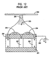
- FIG. 12 shows a planar target type II UBM as presented by Window and Sawides. Window and Harding later disclosed a type II UBM without a central magnetic material or high permeability pole.
- magnets 200 are configured around the periphery of a rectangular or round shunt plate 201.
- Central soft iron pole 207 is located in the center of the shunt plate Because of the 'unbalanced' nature of the magnetic arrangement, a null field point 203 is created above magnetron trap 205 and strengthening field lines above the null point produce a mirror confinement region 208.
- magnetron plasma 204 sputters the target 206. Electrons leaving the magnetron plasma are trapped in the mirror containment region 208 creating a second visible plasma region.
- the mirror plasma region ionizes a significant portion of the sputter flux from the target.
- the plasma 208 generated in the mirror region also projects out to the substrate 209 and usefully bombards the growing sputtered film.
- Plasma 208 can be used for plasma processes such as PECVD, plasma treatment etc. While finding use in these plasma processes, the sputtered flux from the target 206 is not always welcome, the UBM must operate in the mTorr range typical for magnetron sputtering and, for PECVD applications, the exposed target 206 is quickly contaminated by condensing PECVD constituents.
- Hollow Cathode has been used to describe a variety of sputter sources in the prior art.
- U.S. Pat. No. 4,915,805 discloses a hollow cathode confined magnetron with the substrate passing through the center of the cavity.
- U.S. Pat. No. 4,933,057 discloses a hollow cathode configured magnetron with an anode positioned opposite from the opening into the process chamber. The anode in this position will allow electrons to reach the anode without having to pass out of the discharge cavity first. No gas is introduced into the discharge cavity separate from the opening to the process chamber.
- U.S. Pat. No. 5,073,245 teaches a sputter source in a cavity separate from the process chamber.
- the magnetic field is along the axis of the cavity cylinder and a magnetron type containment region is reported to be created around the inside of the cavity cylinder walls.
- the opening to the process chamber creates a discontinuity in the magnetron racetrack.
- Anodes are located inside the cavity, at each end.
- U.S. Pat. No. 5,334,302 discloses a sputtering apparatus comprising multiple magnetron cathode cavities. Process gas is introduced into the base of each cavity. The cavities are open to the process chamber.
- U.S. Pat. No. 5,482,611 discloses an unbalanced magnetron sputter cathode with a cup-shaped or annular cathode. A null magnetic field point is produced adjacent to the cathode opening. The discharge cavity is open to the process chamber.
- a separate microwave applicator is fitted over the cathode opening. Though separate from the cathode, the applicator opening dimensions are equal to or larger than the cathode cavity.
- process gas is introduced into the cavity at the base of the cavity opposite the process chamber opening.
- U.S. Pat. No. 5,908,602 teaches a linear arc discharge source.
- the discharge cavity does not include a magnetron confined plasma region and the discharge cavity opening is exposed to the process chamber.
- U.S. Pat. No. 6,444,100 discloses a box shaped hollow cathode sputter source.
- the bottom of said box is either electrically floating or connected to the cathode.
- the box is open to the process chamber and process gas is not introduced into the box other than via the process chamber opening.
- U.S. Pat. No. 6,444,945 teaches a bipolar plasma source, plasma sheet source, and effusion cell utilizing a bipolar plasma source.
- a magnetron cathode plasma is not created and the hollow cathode cavity opening is exposed to the process chamber.
- U.S. Pat. No. 4,871,918 discloses a hollow-anode ion-electron source comprising a discharge cavity with a reduced dimension opening conduit to the process chamber. There is no magnetron confined region or null magnetic field point within the discharge cavity.
- U.S. Pat. No. 6,103,074 teaches a cathode arc vapor deposition method and apparatus that implements a cusp magnet field. There is no magnetron confined region inside the discharge cavity and the, cavity is open to the process chamber.
- U.S. Appl. No. 2001/0006093 teaches a narrow protruding plasma nozzle on an anode electrode between a plasma generation cavity and a treatment chamber.
- document WO 02/103078A1 discloses a method and device for producing plasma flows of a metal and/or gas, both referring to the use of an unbalanced magnetron magnetic configuration and referring to the use of a balanced magnetron magnetic configuration.
- Applicant's Invention relates to a PECVD apparatus according to claim 1.
- FIG. 1 shows a section view of beam source 24 producing a beam of dense plasma 9 projecting outwardly from nozzle 6.
- Aperture 101 extends through nozzle 6 into discharge cavity 26.
- Discharge cavity 26 has a first width 110.
- Aperture 101 has a second width 115, where the second width 115 is less than the first width 110.
- Center-line 120 comprises the middle of first width 110.
- discharge cavity 26 comprises a parallelepiped having a rectangular cross section. In these embodiments, the first width 110 comprises the length of the longer side of that rectangular cross section. In certain embodiments, discharge cavity 26 a parallelepiped having a square cross section. In these embodiments, the first width 110 comprises the length of one side of that square cross section. In certain embodiments, discharge cavity 26 comprises a cylinder having a circular cross section. In these embodiments, the first width 110 comprises the diameter of that circular cross section.
- aperture 101 has a rectangular cross section. In these embodiments, second width 115 comprises the length of the longer side of that rectangular cross section. In certain embodiments, aperture 101 has a square cross section. In these embodiments, second width 115 comprises the length of one side of that square cross section. In certain embodiments, aperture 101 has a circular cross section. In these embodiments, second width 115 comprises the diameter of that circular cross section.
- Source 24 is disposed within a process chamber, not shown, where that process chamber is maintained at a reduced pressure.
- Magnets 1 and 2 are disposed facing each other with the south poles supported by mild steel shunt 3. By “facing each other,” Applicant means that the pole of magnet 1 having a first magnetic polarity has a facing relationship with the pole of magnet 2 having that same magnetic polarity.
- the magnets 1 and 2 produce a cusp magnetic field composed of outwardly directed field lines 18 and inwardly directed lines 19.
- the inward lines 19 pass through insulator 15 and liner 16 to center shunt 10.
- the cusp magnetic field creates a null magnetic field point 25 inside discharge cavity 26.
- null magnetic field point 25 is located along center-line 120.
- Shunt 10 is connected to shunt 11, and both are made of mild steel. Liner 16 is brazed to block 12 to improve heat transfer.
- Block 12 is water cooled via holes 13 in combination with associated piping not shown.
- Shunt 11 is fastened to block 12.
- the assembly of the liner 16, block 12 and shunts 10 and 11 form one electrode of the source.
- the second electrode is formed by shunt box 3 and cover 5.
- the magnets are ceramic type isolated from liner 16 and block 12 by insulators 14 and 15.
- insulators 14 and 15 are formed from one or more fluoropolymers.
- insulators 14 and 15 are formed from an electrically insulating ceramic material.
- Gap 100 separates separate box 3 from block 12 and shunt 11 to eliminate plasma in the gap.
- gap 100 is about 3 mm.
- Gas 27 is introduced into the source through port 4 in box 3. The gas 27 travels around block 12 via gap 100 between box and block 12. Gas 27 then flows through a plurality of grooves 22 disposed in box 3 and cover 5. Gas 27 is introduced into discharge cavity 26 between cover 5 and liner 16.
- Cover 5 includes a nozzle 6 though which the gas 27 flows into the process chamber.
- the cover 5 and nozzle 6 are water cooled with brazed-on tubing 7.
- One side of power supply 17 is connected to cover 5, box 3, and to chamber ground.
- liner 16 comprises a cathode electrode. In certain embodiments, liner 16 is formed from materials having a secondary electron emission coefficient ⁇ of about 1 or more.
- power supply 17 comprises a standard sputter magnetron type. In certain embodiments, power supply 17 comprises a pulsed DC supply. In certain embodiments, power supply 17 comprises a mid-frequency AC supply. In certain embodiments, power supply 17 comprises an RF supply.
- a DC supply 17 is used with the negative electrode connected to block 12.
- gas 27 is introduced into discharge cavity 26 and power supply 17 is turned on, a plasma is ignited in regions 8 and 9 of the source.
- Region 8 is an endless Hall current contained plasma extending the length of the source.
- the two lobes of region 8, as seen in section view FIG. 1 appear as an extended donut of plasma when the inside of the operating source is viewed.
- This region 8 is created when the electric field from cover 5 penetrates down past magnetic field lines 19 inside the source. As electrons attempt to follow these electric field lines they are restricted by magnetic field lines 19.
- Field lines 18 pass outwardly from liner 16, converge, and pass outwardly through nozzle 6.
- Plasma 9 is created because, when electrons attempt to escape along magnetic field lines 18 through the nozzle 6, they are confronted with a magnetic mirror as field lines 18 converge in nozzle 6. This mirror region reflects a portion of the electrons and creates a second containment region 39 within plasma 9.
- Region 39 is again a closed drift magnetic bottle as electrons move in a cyclodial motion down to one end of the source and back to the other.
- nozzle 6 also forms the only escape path for gas 27 flowing from discharge cavity 26 into the process chamber.
- the process gas 27 is forced through plasma region 39 where a high percentage of gas 27 is ionized prior to exiting nozzle 6.
- the confluence of gas 27 and electrons in region 39 creates a dense plasma 9 that extends outwardly from nozzle 6 into the process chamber.
- plasma 39 and plasma 9 comprise a single plasma.
- the internal diameter of nozzle 6 is smaller than the internal diameter of discharge cavity 26.
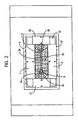
- FIG. 2 shows a top view beam source 24 with cover 5 removed. End magnets 20 and 21, in combination with side magnets 1 and 2, create the closed drift magnetic fields 18 and 19, with only magnetic field 18 shown in FIG. 2.
- FIG. 2 also includes box 3, liner 16, insulator 15 and, below magnets 1, 2, 20 and 21, water cooled block 12. Plurality of grooves 22 in box 3 for gas 27 are also illustrated. Plasma 9 is shown as the darker portion in the center. The lighter portion corresponds to plasma region 39.
- FIG. 3 shows an isometric view of beam source 24 where certain water cooling piping is not shown. As described above, this water piping is useful to make electrical connections to both electrodes.
- plasma 9 emanates outwardly from nozzle 6 into the process chamber. As shown, plasma 9 forms a narrow uniform beam extending outwardly from nozzle 6.
- beam source 24 may comprise many shapes, sizes, scales, and may include a plurality of materials.
- source 24 was constructed as follows: Magnets 1 and 2 were ceramic type measuring about 1" wide x about 4" long x about 1" thick. Magnets 20 and 21 were about 1" wide x about 2" long x about 1" thick. Block 12 was formed from brass. Top cover 5 and nozzle 6 were formed of copper. The opening in nozzle 6 was about 0.75" wide x about 0.75" deep x about 3.5" long. Shunt 10 and shunt 11 were formed of mild steel. Liner 16 was formed of copper sheet bent into an oval shape, with the long internal diameter of that oval measuring about 1.5". As those skilled in the art will appreciate, many variations and modifications can be made regarding the dimensions and materials of source 24 without departing from the scope of Applicant's invention.
- Beam source 24, and the plasma 9 generated therewith have many useful properties, including the following measured values using the source described immediately above:
- Plasma 9 is very dense, with ion densities exceeding 10 12 per cm 3 when using a DC power supply output of 1 kW at 300 V.
- the ion saturation current was measured at over 100 mA for the source dimensions given and these power supply settings.
- the current probe surface was positioned 5 cm beyond the end of nozzle 6 blocking plasma 9. Electron current with the probe grounded is greater than 1 A.
- Plasma 9 is uniform over the length of the source, minus end effects at the turnarounds. This is important for applications where uniformity of deposition, treatment, or etching is required, as it is in most applications. Substrate widths of 3 meters or greater can be uniformly processed. In operation, plasma 9 appears as one cm wide uniform beam extending outwardly from nozzle 6.
- Plasma beam source (“PBS”) 24 is not a sputter source. Rather, source 24 is useful for PECVD, plasma treatment, or etching processes. Although sputtering of the liner material does occur, only minimal amounts of sputtered material exit nozzle 6 for several reasons.
- the magnetron plasma region 8 FIG. 1
- Sputtered liner material redeposits on the liner, the shunts 10 and 11 and/or on the cover 5 and nozzle 6. Because the sputtered material readily condenses upon contact with a surface, source 24 includes a 'torturous path' for sputtered material to exit the source. Second, by feeding process gas into the discharge chamber above magnetron plasma 8, the flow of supply gas to the plasma 8 is directed away from nozzle 6, creating directional momentum effects opposing condensate flow out of nozzle 6.
- a low sputter rate of the source is actually observed in operation.
- a PECVD Silicon Oxide coating after several microns of coating were deposited, the resulting coating appeared optically clear. This clear coating was produced using a copper liner 16.
- sputtered copper in a mixture of oxygen and argon gases comprises a black coating. No such black coating was observed forming a silicon oxide coating on a substrate using source 24.
- Pure reactive gas can be'bumed'in source 24.
- Prior art high density plasma sources implement filaments, low work function materials, or field effect devices, to generate electrons. These sources typically feed an inert gas, such as argon, into the source. Use of a reactive gas such as oxygen inside the source tends to greatly shorten electron source lifetimes. To accomplish a reactive process, these sources feed oxygen into the plasma outside the source, reacting a portion of the oxygen with the argon plasma emanating from the source. While the efficiency of such prior art sources is low, those sources are nevertheless used today for many processes because no alternative exists.
- Applicant's beam source 24 the production of a high density, pure oxygen plasma. This has advantages to several processes. In addition, the vacuum pumping requirements are also reduced because argon flow requirements are not a factor when using source 24.
- Applicant's beam source 24 can be operated over a wide range of process pressures.
- the PBS can readily operate at pressures in the 0,1-10 Pa (1-100 mTorr) region. In addition to this pressure range, operation can be extended down to the 10 -4 Pa (10 -5 Torr) range used in evaporation processes.
- Such pressures may be used because nozzle 6 limits gas conductance out of the source.
- the process gas 27 By feeding the process gas 27 into discharge cavity 26, the pressure inside discharge cavity 26 can be sustained in the 0,1 Pa (mTorr) region, while outside the source the process chamber may be maintained at a much lower pressure. Also, process gas flow requirements are minimized because discharge cavity 26 can be maintained in the required 0,1 Pa (mTorr) region with less gas 27 flow due to the conductance limitation presented by the narrow nozzle 6 opening.
- Plasma beam 9 extends outwardly for 100's of mm from nozzle 6 depending upon the free mean path inside the process chamber. At 0,4 Pa (3 mTorr) for instance, the beam extends at least 300 mm outwardly-from nozzle 6. Formation of such a plasma beam allows beam source 24 to excel at many applications. For instance, non-planar substrates can be uniformly PECVD coated, treated, etc.
- Substrate 23 can be electrically isolated from beam source 24. Because the substrate is not part of the electrical circuit, the substrate can remain floating or be separately biased by a different power supply.
- beam source 24 comprises a standard magnetron power supply using variety of frequencies, including. DC, or AC from 0-100 MHz frequencies. Special high voltage power supplies or RF supplies do not have to be used.
- the connection to chamber ground can also be made to either side of the power supply. In FIGS. 1-3 , box 3 and cover 5 are connected to ground. This is convenient for safety considerations.
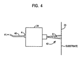
- FIG. 4 shows beam source 24 in a PECVD coating application.
- a mixture of argon and oxygen 41 are delivered to source port 4 via tube 40.
- a monomer gas 43 is released outside the source.
- a polymeric coating is deposited onto substrate 23 by polymerization of monomer gas activated by the ionized gas in plasma 9. Because of the conductance limitation of nozzle 6, and because of the high density and directionality of the plasma 9 exiting through nozzle 6, the monomer gas 43 does not enter source 24. This is actually observed when, after a coating run, the discharge cavity 26 of beam source 24 is essentially free of PECVD coating.
- the substrate 23 can comprise a multitude of materials and shapes. Such substrates include, for example and without limitation, flexible webs, flat glass, three dimensional shapes, metals, silicon wafers, and the like. Other physical and process configurations are possible using beam source 24. For example, one or more monomer gases can be introduced into the discharge cavity 26 without immediate buildup problems. In addition, certain monomer gases, such as hydrocarbons, can be fed into the source for extended periods. Beam source 24 may also perform other plasma processes such as plasma treatment, surface cleaning, or reactive ion etching.
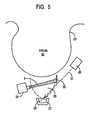
- FIG. 5 shows beam source 24 used to react evaporant 29 in an electron beam evaporation web coating application.
- Drum 25 carries web 23 over the deposition region.
- Crucible 27 contains evaporant material 28.
- Electron beam source 26 projects beam 31 into crucible 27.
- Plasma 9 is directed into the evaporant cloud 29 to promote reaction with the ionized gas of the plasma 9.
- Shield 30 limits the interaction of plasma 9 with the electron beam 31.
- Hollow cathodes are inherently non-uniform as the plasma outside of the hollow cathode is only diffusion limited.
- the magnetic field lines 19 contain the electrons, and by electrostatic forces, the ions are likewise contained in plasma region 9. Also as described above, beam source plasma 9 is uniform over the substrate width due to the closed drift nature of the electron containment.
- FIG. 6 depicts the beam source 24 applied to a planetary box coater application.
- the source 24 is shown along its length rather than from an end view.
- plasma beam 9 appears as a sheet of plasma.
- Source 24 is positioned sufficiently remotely from the substrate supporting planetary, at the bottom of the box coater for example, to allow room for other deposition sources, such as electron beam, or thermal evaporation sources, for instance.
- coatings can be densified by the action of plasma 9.
- pure argon is used to densify a metal coating.
- a reactive gas is added to the argon.
- a major advantage of Applicant's source over the prior art is the ability to directly consume reactive gases, such as oxygen, in the source.
- Prior art sources due to the need for filaments or other electron generation means sensitive to consumption by a reactive gas, required the use of an inert gas in the source.
- the reactive gas was fed into the process chamber external to the source. The necessarily poor efficiency of ionizing the reactive gas in the chamber rather than in the source itself requires high source powers and high argon flow rates.
- using beam source 24 to produce a pure reactive plasma, or a combination of inert and reactive as required process efficiency is increased and the overall pumping speed needed to maintain the process at the correct pressure is reduced. As those skilled in the art will appreciate, excess argon need not be pumped away.
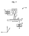
- FIG. 7 shows beam source 24 disposed above a substrate 23, such as a silicon wafer.
- the stage 51 supporting the wafer 23 is translated, i.e. moved, in the X and/or Y directions to uniformly treat wafer 23 with plasma 9.
- Bias supply 52 in this case an AC supply of sufficient frequency to pass current through the wafer 23, is connected to stage 51.
- Beam source supply 17 produces plasma 9.
- the insulating substrate 23 would normally rise to the characteristic floating voltage of plasma 9, i.e. typically between about -10 to about -70 volts for the beam source 24 depending upon process conditions.
- bias supply 52 By turning on bias supply 52, the voltage drop across the plasma dark space between the plasma 9 and substrate 23 can be changed, positively or negatively, to a level required for the process. Because the substrate 23 is not an electrode in beam source 24, it can be separately biased.
- FIG. 8 shows two beam sources, 24a and 24b, used to a generate a large area uniform plasma 91 over a substrate.
- the substrate comprises flexible web 23 drawn over roll 64.
- the two beam sources 24a and 24b are identical, except magnets 60 and 61 of source 24a, and the end magnets (not shown) in source 24a are disposed such that the south pole has a facing relationship with plasma 91, while source 24b has magnet 62 and 63 north poles facing inwardly. This configuration creates a sharing of magnetic fields between the sources and produces the closed plasma region 91 as shown.
- FIG. 9 shows a section view of source 90 configured for a space propulsion application.
- the basic components of the magnetron electron source and cusp magnetic field are the same as in earlier figures.
- the magnetic cusp fields 18 and 19 are created by annular electro-magnets 70 and 71.
- the electron source magnetron plasma 8 is created within the liner tube 16.
- Liner 16 is electrically isolated from box 3 by insulator plate 72 and from electromagnet 71 by insulator ring 73.
- the propellant gas 27 is introduced into gas cavity 79 through port 92. Gas 27 then flows into discharge cavity 26 via gap 78 between liner 16 and opposed electrode 5.
- Cover electrode 5 is electrically isolated from round box 3 by insulator plate 76. Cover 5 has a nozzle portion 6 that fits down into the annular opening in electromagnet 70. Liner 16 and cover 5 are connected across power supply 74.
- the illustrated embodiment of FIG. 11 includes a DC supply with the cathode terminal connected to liner 16. In other embodiments, an AC or RF power supply is used. Box 3 is connect to ground.
- power supply 74 is turned on, and gas 27 is flowing into discharge cavity 26, electrons created by magnetron plasma 8 are trapped in mirror field region of magnetic field 18, and plasmas 9 and 39 are created. Thrust is generated as the plasma 9 is expelled through nozzle 6.
- One component of the thrust is generated by the magnetic nozzle effect. After passing through magnetic mirror 39, electrons then experience a decrease in magnetic field strength as they move outwardly from nozzle 6. In response to this negative gradient field, electron motion is converted from thermal spinning to kinetic motion along the axis of the field lines.
- the electrons in turn electrostatically pull ions into accelerating away from the source.
- Another form of ion thrust is produced if the magnetic field in region 18 is increased to confine ions, i.e. to a magnetic field strength exceeding at least 1000 Gauss. Under this condition, ions are magnetically confined and heated by the radial electric field as they pass through nozzle 6. As those electrons exit the nozzle, they are accelerated by both the electrostatic repulsion from anode 5 and by the magnetic nozzle effect.
- the electron confinement achieved using Applicant's source includes physically limiting two of the possible three axial magnetic field electron escape paths by liner 16.
- the three axial magnetic field regions include: (i) cone shaped compressed region 18, (ii) cone-shaped compressed region 19, and (iii) planar disk compressed region 170.
- liner 16 When liner 16 is connected as the cathode of a DC circuit, or is on a negative AC cycle of an AC power supply, electrons are electrostatically reflected from the liner's surfaces. As electrons attempt to reach the anode electrode 5, they travel by collisional diffusion across field lines 19 and through mirror region 39 to exit the source through nozzle 6 before returning to cover 5. While diffusing across magnetic field lines, the electrons also spiral along these field lines.
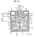
- FIG. 10 shows beam source 100.
- source 100 is circular, annular, or extended length wise.
- source 100 includes rare earth magnets 1 and 2, and two power supplies 83 and 84.
- Power supply 83 connects cathode liner 16 to box 3.
- Insulator 81 separate box 3 electrically from cover 5.
- Power supply 84 connects anode cover 5 to box 3. Box three is grounded.
- FIG. 10 further illustrates process gas manifolds 80 built into cover 5. Small distribution holes 85 conduct the gas 27 uniformly along the length of source 100 into discharge cavity 26. Facing the magnets 1 and 2 toward each other in a cusp arrangement, creates a strong mirror compression ratio in mirror region 39. With rare earth magnets 1 and 2, the field strength at the mirror apex can exceed 500 Gauss. As electrons pass through this mirror region 39, they experience this strong field and their Larmor gyro radius is correspondingly small. Under these conditions, when the plasma is viewed from the end as in this section view, the plasma 9 width passing through nozzle 6 is very narrow, on the order of 3 mm.
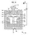
- FIG. 11 A vertical magnet orientation is shown in another preferred embodiment in FIG. 11 .
- the field strength is typically less than 100 Gauss and the electron Larmor gyro radius is larger.
- shunt 10 is fitted into aluminum body 12. Shunt 10 reduces the sputter rate of liner 16, and evens out liner 16 sputtering to make the liner 16 last longer. While helpful in this regard, shunt 10 is not necessary to the fundamental source operation.
- Body 12 is water cooled by extruded holes 82.
- Insulators 14 and 86 support cathode body 12 in box 3 and electrically isolate the cathode, i.e. body 12 and liner 16, from box 3.
- Source 100 may be rectangular having an extended length. End magnets, used to make both magnetic field regions 8 and 9 closed paths, are not shown in FIG. 10 .
- FIG. 11 shows beam source 1100 having vertically oriented magnets.
- This magnet configuration is representative of a Type II unbalanced magnetron magnetic field as taught by Window and Harding.
- a range of magnet 97 shapes, and discharge cavity 26 shapes, can be implemented within the scope of Applicant's invention.
- magnets 97 create two confinement regions: magnetron confinement 95 at cathode 98 surface 105, and mirror / nozzle confinement 93 through nozzle 104.
- a magnetron electron generation region 101 is contained in a discharge cavity 103.
- the discharge cavity contains a null magnetic field region 95.
- a aperture 104 in cover plate 91 has a centerline coincident with the axis of mirror field 93.
- Planar liner 98 is water cooled via gun drilled hole 99 and is fitted into shunt 96. Magnets 97 and angled shunts 109, along with shunt 96 produce the unbalanced magnetic field depicted. Planar cathode 98 and magnet components 96, 97 and 109 are suspended by electrical insulators (not shown) in electrically floating box 90. Electrically floating cover plate 91 is fastened to box 90. Cover plate 91 is water cooled via holes 92. Piping to direct water to the cover plate 91 and cathode 98 is not shown. Gas 27 is piped into box 90 through threaded hole 100. Gas 27 flows around magnet shunt 96 and into discharge cavity 103.
- FIG. 11 includes a separate anode 107.
- Cover 91 is not connected as an electrode in the electrical circuit. Cover 91 comprises a conductance limitation to the exiting gas 27, forcing the gas to exit through the mirror confinement region 106 in nozzle 104. Given the high mobility of electrons, positioning the return electrode 107 external to the source produces little noticeable change in source performance after the source lights. Because the anode 107 is more distant from the cathode 98, a pressure spike may be needed in cavity 103, depending upon the base pressure and the ignition voltage of the power supply 108 used, to ignite the plasma 102.
- the anode electrode can be located in any location within the process chamber.
- the anode electrode is the nozzle 104, some ion acceleration benefits can be obtained as described earlier.
- the liner material comprises aluminum.
- Aluminum is a good secondary electron emitter when oxygen gas 27 is used.
- the reactive product, alumina, formed on the cathode surface 105 sputters very slowly.
- FIG. 11 is a section view.
- Source 1100 can be round, or rectangular, and can be extended to lengths longer than 1 meter. The present invention enables many applications and processes; Several have been mentioned above. More will be apparent to those skilled in the art. While several embodiments have been presented, many others are possible within the scope of the present invention.
Landscapes
- Physics & Mathematics (AREA)
- Engineering & Computer Science (AREA)
- Plasma & Fusion (AREA)
- Chemical & Material Sciences (AREA)
- Analytical Chemistry (AREA)
- Spectroscopy & Molecular Physics (AREA)
- Electromagnetism (AREA)
- Combustion & Propulsion (AREA)
- Plasma Technology (AREA)
- Chemical Vapour Deposition (AREA)
- Drying Of Semiconductors (AREA)
- Physical Vapour Deposition (AREA)
- Electron Sources, Ion Sources (AREA)
Claims (11)
- Appareil à dépôt chimique en phase vapeur activé par plasma (PECVD) comprenant une chambre de traitement pour traiter un substrat (23) et une source de faisceau plasma (24) qui comprend:une cavité de décharge (26) ayant une première largeur (110), ladite cavité de décharge (26) comprenant une partie supérieure (5) et une partie de paroi (16);une première alimentation électrique (17);au moins une électrode de cathode connectée à ladite première alimentation électrique (17), ladite électrode de cathode étant capable de soutenir au moins une région de décharge magnétron à l'intérieur de ladite cavité de décharge (26) ;un conduit disposé dans ladite cavité de décharge (26) pour introduire un gaz ionisable (27) dans ladite cavité de décharge (26);une buse (6) disposée sur ladite partie supérieure (5) ets'étendant vers l'extérieur de celle-ci, ladite buse (6) étant formée pour inclure une ouverture (101), autre que ledit conduit, s'étendant à travers ladite partie supérieure et dans ladite cavité de décharge, ladite ouverture (101) ayant une deuxième largeur (115) qui est inférieure à ladite première largeur (110), etune pluralité d'aimants (1, 2, 20, 21) disposés adjacents à ladite partie de paroi (16);dans lequel du plasma (9) provenant de ladite cavité de décharge (26) passe à travers ladite ouverture (101) deladite buse (6) dans ladite chambre de traitement;
ledit appareil comprenant en outre des moyens pour libérer un gaz monomère (43) à l'extérieur de ladite source de faisceau plasma (24), de sorte que du plasma (9) passant à travers ladite ouverture (101) de ladite buse (6) permet un revêtement PECVD sur ledit substrat (23) par polymérisation dudit gaz monomère; caractérisé en ce que
la pluralité d'aimants (1, 2, 20, 21) crée un point de champ magnétique nul (25) à l'intérieur de ladite cavité de décharge ainsi qu'un miroir magnétique lorsque les lignes de champ convergent dans ladite buse (6). - Appareil PECVD selon la revendication 1, dans lequel lesdits aimants (1, 2, 20, 21) sont disposés adjacents à ladite partie de paroi (16) et disposés en face les uns des autres, un pôle de chacun desdits aimants (1, 2, 20, 21) ayant une première polarité magnétique étant orienté vers l'intérieur de ladite cavité de décharge (26), le pôle opposé de chacun desdits aimants (1, 2, 20, 21) ayant une seconde polarité magnétique étant orienté vers l'extérieur de la cavité de décharge (26).
- Appareil PECVD selon la revendication 1, dans lequel ledit gaz ionisable (27) est injecté entre ladite cathode et ladite buse (6) à l'intérieur de ladite cavité de décharge (26).
- Appareil PECVD selon la revendication 1, dans lequel ladite pluralité d'aimants (1, 2, 20, 21) comprend deux ou plusieurs électro-aimants.
- Appareil PECVD selon la revendication 1, dans lequel deux des trois régions axiales de champ magnétique adjactents au point nul (25) passent à travers la surface de ladite cathode, et dans lequel un troisième champ magnétique axial comprend le miroir magnétique à travers ladite buse (6).
- Appareil PECVD selon la revendication 1, dans lequel ledit point de champ magnétique nul (25) est situé sur la ligne médiane (120) de ladite ouverture (101).
- Appareil PECVD selon la revendication 1, dans lequel le matériau de ladite cathode comprend un coefficient d'émission d'électrons secondaires (8) supérieur à environ 1 dans des conditions de production de plasma.
- Appareil PECVD selon la revendication 1, dans lequel ladite buse (6) est interconnecté avec ladite première alimentation électrique (17) de telle sorte que ladite buse (6) comprend une anode.
- Appareil PECVD selon la revendication 1, dans lequel ladite buse (6) est électriquement flottante.
- Appareil PECVD selon la revendication 1, dans lequel ladite buse (6) est reliée électriquement à la masse.
- Appareil PECVD selon la revendication 1, comprenant en outre une deuxième alimentation électrique, ladite deuxième alimentation électrique étant reliée à ladite buse (6) de telle sorte que ladite buse (6) comprend une anode.
Applications Claiming Priority (3)
| Application Number | Priority Date | Filing Date | Title |
|---|---|---|---|
| US41205102P | 2002-09-19 | 2002-09-19 | |
| US412051P | 2002-09-19 | ||
| PCT/US2003/029204 WO2004027825A2 (fr) | 2002-09-19 | 2003-09-19 | Source de plasma a faisceau |
Publications (3)
| Publication Number | Publication Date |
|---|---|
| EP1554412A2 EP1554412A2 (fr) | 2005-07-20 |
| EP1554412A4 EP1554412A4 (fr) | 2010-03-10 |
| EP1554412B1 true EP1554412B1 (fr) | 2013-08-14 |
Family
ID=32030790
Family Applications (1)
| Application Number | Title | Priority Date | Filing Date |
|---|---|---|---|
| EP03756819.3A Expired - Lifetime EP1554412B1 (fr) | 2002-09-19 | 2003-09-19 | Appareil de dépôt chimique en phase vapeur assisté par plasma |
Country Status (5)
| Country | Link |
|---|---|
| US (1) | US7327089B2 (fr) |
| EP (1) | EP1554412B1 (fr) |
| JP (2) | JP5160730B2 (fr) |
| AU (1) | AU2003299015A1 (fr) |
| WO (1) | WO2004027825A2 (fr) |
Cited By (1)
| Publication number | Priority date | Publication date | Assignee | Title |
|---|---|---|---|---|
| WO2016069807A1 (fr) | 2014-10-29 | 2016-05-06 | Ppg Industries Ohio, Inc. | Système de revêtement protecteur pour un substrat en matière plastique |
Families Citing this family (39)
| Publication number | Priority date | Publication date | Assignee | Title |
|---|---|---|---|---|
| US7411352B2 (en) * | 2002-09-19 | 2008-08-12 | Applied Process Technologies, Inc. | Dual plasma beam sources and method |
| FR2857555B1 (fr) * | 2003-07-09 | 2005-10-14 | Snecma Moteurs | Accelerateur a plasma a derive fermee d'electrons |
| US7312579B2 (en) * | 2006-04-18 | 2007-12-25 | Colorado Advanced Technology Llc | Hall-current ion source for ion beams of low and high energy for technological applications |
| EP2188411B1 (fr) * | 2007-08-30 | 2011-10-26 | Koninklijke Philips Electronics N.V. | Système de pulvérisation cathodique |
| DE102008028542B4 (de) * | 2008-06-16 | 2012-07-12 | Fraunhofer-Gesellschaft zur Förderung der angewandten Forschung e.V. | Verfahren und Vorrichtung zum Abscheiden einer Schicht auf einem Substrat mittels einer plasmagestützten chemischen Reaktion |
| TWI641292B (zh) | 2008-08-04 | 2018-11-11 | Agc北美平面玻璃公司 | 電漿源 |
| DE102009037853B3 (de) * | 2009-08-18 | 2011-03-31 | Fraunhofer-Gesellschaft zur Förderung der angewandten Forschung e.V. | Gasflusssputterquelle |
| JPWO2012172630A1 (ja) * | 2011-06-13 | 2015-02-23 | トヨタ自動車株式会社 | 表面加工装置及び表面加工方法 |
| US8617350B2 (en) | 2011-06-15 | 2013-12-31 | Belight Technology Corporation, Limited | Linear plasma system |
| US9761424B1 (en) | 2011-09-07 | 2017-09-12 | Nano-Product Engineering, LLC | Filtered cathodic arc method, apparatus and applications thereof |
| US10304665B2 (en) | 2011-09-07 | 2019-05-28 | Nano-Product Engineering, LLC | Reactors for plasma-assisted processes and associated methods |
| DE102011112759A1 (de) * | 2011-09-08 | 2013-03-14 | Oerlikon Trading Ag, Trübbach | Plasmaquelle |
| CN102523673A (zh) * | 2011-12-19 | 2012-06-27 | 北京大学 | 一种采用磁镜场约束的等离子体密封窗及其密封方法 |
| US10056237B2 (en) | 2012-09-14 | 2018-08-21 | Vapor Technologies, Inc. | Low pressure arc plasma immersion coating vapor deposition and ion treatment |
| US9412569B2 (en) | 2012-09-14 | 2016-08-09 | Vapor Technologies, Inc. | Remote arc discharge plasma assisted processes |
| US9793098B2 (en) | 2012-09-14 | 2017-10-17 | Vapor Technologies, Inc. | Low pressure arc plasma immersion coating vapor deposition and ion treatment |
| CN105008585A (zh) * | 2012-12-28 | 2015-10-28 | 零件喷涂公司 | 等离子体增强的化学气相沉积(pecvd)源 |
| KR101797157B1 (ko) | 2013-02-06 | 2017-11-13 | 아르셀러미탈 인베스티가시온 와이 데살롤로 에스엘 | 플라즈마 소스 |
| US10134557B2 (en) * | 2013-06-12 | 2018-11-20 | General Plasma, Inc. | Linear anode layer slit ion source |
| JP6403269B2 (ja) * | 2014-07-30 | 2018-10-10 | 株式会社神戸製鋼所 | アーク蒸発源 |
| US9968016B2 (en) * | 2014-08-11 | 2018-05-08 | Toyota Motor Engineering & Manufacturing North America, Inc. | Magnetic field shield |
| CN104411082B (zh) * | 2014-11-12 | 2017-12-19 | 中国科学院深圳先进技术研究院 | 等离子源系统和等离子生成方法 |
| JP6508746B2 (ja) | 2014-12-05 | 2019-05-08 | エージーシー フラット グラス ノース アメリカ,インコーポレイテッドAgc Flat Glass North America,Inc. | マクロ粒子低減コーティングを利用したプラズマ源ならびにマクロ粒子低減コーティングを用いたプラズマ源を薄膜コーティングおよび表面改質に使用する方法 |
| MX2017007356A (es) | 2014-12-05 | 2018-04-11 | Agc Flat Glass Europe S A | Fuente de plasma del catodo hueco. |
| US9721764B2 (en) | 2015-11-16 | 2017-08-01 | Agc Flat Glass North America, Inc. | Method of producing plasma by multiple-phase alternating or pulsed electrical current |
| US9721765B2 (en) | 2015-11-16 | 2017-08-01 | Agc Flat Glass North America, Inc. | Plasma device driven by multiple-phase alternating or pulsed electrical current |
| US10192708B2 (en) * | 2015-11-20 | 2019-01-29 | Oregon Physics, Llc | Electron emitter source |
| US10242846B2 (en) | 2015-12-18 | 2019-03-26 | Agc Flat Glass North America, Inc. | Hollow cathode ion source |
| US10573499B2 (en) | 2015-12-18 | 2020-02-25 | Agc Flat Glass North America, Inc. | Method of extracting and accelerating ions |
| US10227691B2 (en) | 2015-12-21 | 2019-03-12 | IonQuest LLC | Magnetically enhanced low temperature-high density plasma-chemical vapor deposition plasma source for depositing diamond and diamond like films |
| US11823859B2 (en) | 2016-09-09 | 2023-11-21 | Ionquest Corp. | Sputtering a layer on a substrate using a high-energy density plasma magnetron |
| US11359274B2 (en) | 2015-12-21 | 2022-06-14 | IonQuestCorp. | Electrically and magnetically enhanced ionized physical vapor deposition unbalanced sputtering source |
| US11482404B2 (en) | 2015-12-21 | 2022-10-25 | Ionquest Corp. | Electrically and magnetically enhanced ionized physical vapor deposition unbalanced sputtering source |
| US10957519B2 (en) | 2015-12-21 | 2021-03-23 | Ionquest Corp. | Magnetically enhanced high density plasma-chemical vapor deposition plasma source for depositing diamond and diamond-like films |
| WO2019154490A1 (fr) * | 2018-02-07 | 2019-08-15 | Applied Materials, Inc. | Appareil de dépôt, procédé de revêtement d'un substrat souple et substrat souple muni d'un revêtement |
| US11834204B1 (en) | 2018-04-05 | 2023-12-05 | Nano-Product Engineering, LLC | Sources for plasma assisted electric propulsion |
| TWI686106B (zh) * | 2019-01-25 | 2020-02-21 | 國立清華大學 | 場發射手持式常壓電漿產生裝置 |
| WO2020198012A1 (fr) * | 2019-03-26 | 2020-10-01 | Board Of Trustees Of Michigan State University | Source de plasma à faisceau unique |
| CN113365402B (zh) * | 2020-03-06 | 2023-04-07 | 上海宏澎能源科技有限公司 | 限制等离子束的装置 |
Citations (3)
| Publication number | Priority date | Publication date | Assignee | Title |
|---|---|---|---|---|
| US5304279A (en) * | 1990-08-10 | 1994-04-19 | International Business Machines Corporation | Radio frequency induction/multipole plasma processing tool |
| US6196155B1 (en) * | 1998-04-15 | 2001-03-06 | Hitachi, Ltd. | Plasma processing apparatus and method of cleaning the apparatus |
| US6444945B1 (en) * | 2001-03-28 | 2002-09-03 | Cp Films, Inc. | Bipolar plasma source, plasma sheet source, and effusion cell utilizing a bipolar plasma source |
Family Cites Families (45)
| Publication number | Priority date | Publication date | Assignee | Title |
|---|---|---|---|---|
| US3878085A (en) * | 1973-07-05 | 1975-04-15 | Sloan Technology Corp | Cathode sputtering apparatus |
| US4529571A (en) * | 1982-10-27 | 1985-07-16 | The United States Of America As Represented By The United States Department Of Energy | Single-ring magnetic cusp low gas pressure ion source |
| US4727293A (en) * | 1984-08-16 | 1988-02-23 | Board Of Trustees Operating Michigan State University | Plasma generating apparatus using magnets and method |
| YU46728B (sh) * | 1986-10-23 | 1994-04-05 | VUJO dr. MILJEVIĆ | Jonsko-elektronski izvor sa šupljom anodom |
| US4868003A (en) * | 1986-11-26 | 1989-09-19 | Optical Coating Laboratory, Inc. | System and method for vacuum deposition of thin films |
| JPS63274762A (ja) * | 1987-05-01 | 1988-11-11 | Ulvac Corp | 反応蒸着膜の形成装置 |
| ZA884511B (en) * | 1987-07-15 | 1989-03-29 | Boc Group Inc | Method of plasma enhanced silicon oxide deposition |
| IT1211938B (it) * | 1987-11-27 | 1989-11-08 | Siv Soc Italiana Vetro | Apparecchiatura e procedimento per la deposizione di uno strato sottile su un substrato trasparente, particolarmente per la realizzazione di vetrature |
| US4915805A (en) * | 1988-11-21 | 1990-04-10 | At&T Bell Laboratories | Hollow cathode type magnetron apparatus construction |
| DE4026367A1 (de) * | 1990-06-25 | 1992-03-12 | Leybold Ag | Vorrichtung zum beschichten von substraten |
| US5073245A (en) * | 1990-07-10 | 1991-12-17 | Hedgcoth Virgle L | Slotted cylindrical hollow cathode/magnetron sputtering device |
| US5069770A (en) * | 1990-07-23 | 1991-12-03 | Eastman Kodak Company | Sputtering process employing an enclosed sputtering target |
| DE4042286C1 (fr) * | 1990-12-31 | 1992-02-06 | Leybold Ag, 6450 Hanau, De | |
| DE69216685T2 (de) * | 1991-05-31 | 1997-05-28 | Deposition Sciences Inc | Sputteranlage |
| US5482611A (en) * | 1991-09-30 | 1996-01-09 | Helmer; John C. | Physical vapor deposition employing ion extraction from a plasma |
| US5334302A (en) * | 1991-11-15 | 1994-08-02 | Tokyo Electron Limited | Magnetron sputtering apparatus and sputtering gun for use in the same |
| JPH06128730A (ja) * | 1992-10-20 | 1994-05-10 | Nikon Corp | 金属薄膜の製造方法 |
| DE4236264C1 (fr) * | 1992-10-27 | 1993-09-02 | Fraunhofer-Gesellschaft Zur Foerderung Der Angewandten Forschung Ev, 80636 Muenchen, De | |
| FR2701797B1 (fr) * | 1993-02-18 | 1995-03-31 | Commissariat Energie Atomique | Coupleur de transfert d'une puissance micro-onde vers une nappe de plasma et source micro-onde linéaire pour le traitement de surfaces par plasma . |
| JPH0765764A (ja) * | 1993-08-28 | 1995-03-10 | Ulvac Japan Ltd | シートイオンビーム装置 |
| JP2876280B2 (ja) * | 1993-12-27 | 1999-03-31 | 住友重機械工業株式会社 | ビーム発生方法及び装置 |
| JP2909696B2 (ja) * | 1993-12-21 | 1999-06-23 | 住友重機械工業株式会社 | ビーム発生方法及び装置 |
| SE9403988L (sv) * | 1994-11-18 | 1996-04-01 | Ladislav Bardos | Apparat för alstring av linjär ljusbågsurladdning för plasmabearbetning |
| RU2084085C1 (ru) * | 1995-07-14 | 1997-07-10 | Центральный научно-исследовательский институт машиностроения | Ускоритель с замкнутым дрейфом электронов |
| JPH09228038A (ja) * | 1996-02-23 | 1997-09-02 | Balzers Prozes Syst Gmbh | 中空のターゲットを備えた、陰極スパッタによりサブストレートを被覆するための装置 |
| US6137231A (en) * | 1996-09-10 | 2000-10-24 | The Regents Of The University Of California | Constricted glow discharge plasma source |
| JP4043089B2 (ja) * | 1997-02-24 | 2008-02-06 | 株式会社エフオーアイ | プラズマ処理装置 |
| US6103074A (en) | 1998-02-14 | 2000-08-15 | Phygen, Inc. | Cathode arc vapor deposition method and apparatus |
| AUPP479298A0 (en) * | 1998-07-21 | 1998-08-13 | Sainty, Wayne | Ion source |
| JP2965293B1 (ja) * | 1998-11-10 | 1999-10-18 | 川崎重工業株式会社 | 電子ビーム励起プラズマ発生装置 |
| DE10060002B4 (de) * | 1999-12-07 | 2016-01-28 | Komatsu Ltd. | Vorrichtung zur Oberflächenbehandlung |
| US6444100B1 (en) * | 2000-02-11 | 2002-09-03 | Seagate Technology Llc | Hollow cathode sputter source |
| JP3865570B2 (ja) * | 2000-06-16 | 2007-01-10 | 伊藤光学工業株式会社 | プラズマ加工法 |
| US6446572B1 (en) * | 2000-08-18 | 2002-09-10 | Tokyo Electron Limited | Embedded plasma source for plasma density improvement |
| US6911779B2 (en) * | 2001-04-20 | 2005-06-28 | John Madocks | Magnetic mirror plasma source |
| US20020153103A1 (en) * | 2001-04-20 | 2002-10-24 | Applied Process Technologies, Inc. | Plasma treatment apparatus |
| US7023128B2 (en) * | 2001-04-20 | 2006-04-04 | Applied Process Technologies, Inc. | Dipole ion source |
| US7294283B2 (en) * | 2001-04-20 | 2007-11-13 | Applied Process Technologies, Inc. | Penning discharge plasma source |
| SE525231C2 (sv) * | 2001-06-14 | 2005-01-11 | Chemfilt R & D Ab | Förfarande och anordning för att alstra plasma |
| US7025833B2 (en) * | 2002-02-27 | 2006-04-11 | Applied Process Technologies, Inc. | Apparatus and method for web cooling in a vacuum coating chamber |
| US6919672B2 (en) * | 2002-04-10 | 2005-07-19 | Applied Process Technologies, Inc. | Closed drift ion source |
| CH707466B1 (de) | 2002-10-03 | 2014-07-15 | Tetra Laval Holdings & Finance | Vorrichtung zur Durchführung eines Plasma-unterstützten Prozesses. |
| US7259378B2 (en) * | 2003-04-10 | 2007-08-21 | Applied Process Technologies, Inc. | Closed drift ion source |
| US7038389B2 (en) * | 2003-05-02 | 2006-05-02 | Applied Process Technologies, Inc. | Magnetron plasma source |
| EP1774563A1 (fr) | 2004-07-01 | 2007-04-18 | Cardinal CG Company | Cible cylindrique a aimant oscillant pour pulverisation cathodique magnetron |
-
2003
- 2003-09-19 EP EP03756819.3A patent/EP1554412B1/fr not_active Expired - Lifetime
- 2003-09-19 AU AU2003299015A patent/AU2003299015A1/en not_active Abandoned
- 2003-09-19 WO PCT/US2003/029204 patent/WO2004027825A2/fr active Application Filing
- 2003-09-19 US US10/528,386 patent/US7327089B2/en not_active Expired - Fee Related
- 2003-09-19 JP JP2004537902A patent/JP5160730B2/ja not_active Expired - Fee Related
-
2012
- 2012-01-13 JP JP2012005596A patent/JP5642721B2/ja not_active Expired - Fee Related
Patent Citations (3)
| Publication number | Priority date | Publication date | Assignee | Title |
|---|---|---|---|---|
| US5304279A (en) * | 1990-08-10 | 1994-04-19 | International Business Machines Corporation | Radio frequency induction/multipole plasma processing tool |
| US6196155B1 (en) * | 1998-04-15 | 2001-03-06 | Hitachi, Ltd. | Plasma processing apparatus and method of cleaning the apparatus |
| US6444945B1 (en) * | 2001-03-28 | 2002-09-03 | Cp Films, Inc. | Bipolar plasma source, plasma sheet source, and effusion cell utilizing a bipolar plasma source |
Non-Patent Citations (1)
| Title |
|---|
| "Plasma-enhanced chemical vapor deposition", WIKIPEDIA, THE FREE ENCYCLOPEDIA, 7 April 2011 (2011-04-07), XP055039279, Retrieved from the Internet <URL:http://en.wikipedia.org/w/index.php?title=Plasma-enhanced_chemical_vapor_deposition& oldid=422860331> [retrieved on 20120926] * |
Cited By (1)
| Publication number | Priority date | Publication date | Assignee | Title |
|---|---|---|---|---|
| WO2016069807A1 (fr) | 2014-10-29 | 2016-05-06 | Ppg Industries Ohio, Inc. | Système de revêtement protecteur pour un substrat en matière plastique |
Also Published As
| Publication number | Publication date |
|---|---|
| JP5160730B2 (ja) | 2013-03-13 |
| AU2003299015A1 (en) | 2004-04-08 |
| EP1554412A2 (fr) | 2005-07-20 |
| EP1554412A4 (fr) | 2010-03-10 |
| WO2004027825A3 (fr) | 2005-04-28 |
| AU2003299015A8 (en) | 2004-04-08 |
| WO2004027825A2 (fr) | 2004-04-01 |
| JP5642721B2 (ja) | 2014-12-17 |
| US7327089B2 (en) | 2008-02-05 |
| US20060152162A1 (en) | 2006-07-13 |
| JP2006500740A (ja) | 2006-01-05 |
| JP2012124168A (ja) | 2012-06-28 |
Similar Documents
| Publication | Publication Date | Title |
|---|---|---|
| EP1554412B1 (fr) | Appareil de dépôt chimique en phase vapeur assisté par plasma | |
| US7411352B2 (en) | Dual plasma beam sources and method | |
| EP0328076B1 (fr) | Appareil pour former des films minces et source d'ions utilisant la pulvérisation par plasma micro-onde | |
| US6214183B1 (en) | Combined ion-source and target-sputtering magnetron and a method for sputtering conductive and nonconductive materials | |
| US7932678B2 (en) | Magnetic mirror plasma source and method using same | |
| US9136086B2 (en) | Closed drift magnetic field ion source apparatus containing self-cleaning anode and a process for substrate modification therewith | |
| US6238537B1 (en) | Ion assisted deposition source | |
| US5457298A (en) | Coldwall hollow-cathode plasma device for support of gas discharges | |
| CA2326202C (fr) | Procede et appareil pour deposer des revetements a texture biaxiale | |
| US20090200158A1 (en) | High power impulse magnetron sputtering vapour deposition | |
| US20070205096A1 (en) | Magnetron based wafer processing | |
| US20040020760A1 (en) | Pulsed highly ionized magnetron sputtering | |
| JPS6254078A (ja) | 陰極スパツタリング処理により基板に薄層を被着する装置 | |
| JPS5845892B2 (ja) | スパツタ蒸着装置 | |
| US7038389B2 (en) | Magnetron plasma source | |
| EP0523695B1 (fr) | Appareillage de pulvérisation cathodique et source d'ions | |
| RU2373603C1 (ru) | Источник быстрых нейтральных атомов | |
| US11049697B2 (en) | Single beam plasma source | |
| JP2849771B2 (ja) | スパッタ型イオン源 | |
| US20220013324A1 (en) | Single beam plasma source | |
| RU2248064C1 (ru) | Источник ионов | |
| GB2360530A (en) | High target utilisation sputtering system with remote plasma source | |
| JPS6396283A (ja) | イオン源 | |
| JPH01201467A (ja) | イオン源 | |
| SE537187C2 (sv) | Magnetronplasmaapparat förstärkt genom hålkatodplasma |
Legal Events
| Date | Code | Title | Description |
|---|---|---|---|
| PUAI | Public reference made under article 153(3) epc to a published international application that has entered the european phase |
Free format text: ORIGINAL CODE: 0009012 |
|
| 17P | Request for examination filed |
Effective date: 20050418 |
|
| AK | Designated contracting states |
Kind code of ref document: A2 Designated state(s): AT BE BG CH CY CZ DE DK EE ES FI FR GB GR HU IE IT LI LU MC NL PT RO SE SI SK TR |
|
| AX | Request for extension of the european patent |
Extension state: AL LT LV MK |
|
| DAX | Request for extension of the european patent (deleted) | ||
| A4 | Supplementary search report drawn up and despatched |
Effective date: 20100204 |
|
| RIC1 | Information provided on ipc code assigned before grant |
Ipc: H01J 27/14 20060101ALI20100129BHEP Ipc: F03H 1/00 20060101ALI20100129BHEP Ipc: C23C 16/00 20060101AFI20050506BHEP |
|
| 17Q | First examination report despatched |
Effective date: 20100924 |
|
| RAP1 | Party data changed (applicant data changed or rights of an application transferred) |
Owner name: GENERAL PLASMA, INC. |
|
| REG | Reference to a national code |
Ref country code: DE Ref legal event code: R079 Ref document number: 60344740 Country of ref document: DE Free format text: PREVIOUS MAIN CLASS: C23C0016000000 Ipc: H01J0027140000 |
|
| GRAP | Despatch of communication of intention to grant a patent |
Free format text: ORIGINAL CODE: EPIDOSNIGR1 |
|
| RIC1 | Information provided on ipc code assigned before grant |
Ipc: H01J 37/32 20060101ALI20130201BHEP Ipc: H01J 27/14 20060101AFI20130201BHEP Ipc: H05H 1/48 20060101ALI20130201BHEP Ipc: C23C 16/513 20060101ALI20130201BHEP |
|
| GRAS | Grant fee paid |
Free format text: ORIGINAL CODE: EPIDOSNIGR3 |
|
| GRAA | (expected) grant |
Free format text: ORIGINAL CODE: 0009210 |
|
| AK | Designated contracting states |
Kind code of ref document: B1 Designated state(s): AT BE BG CH CY CZ DE DK EE ES FI FR GB GR HU IE IT LI LU MC NL PT RO SE SI SK TR |
|
| REG | Reference to a national code |
Ref country code: GB Ref legal event code: FG4D |
|
| REG | Reference to a national code |
Ref country code: CH Ref legal event code: EP Ref country code: AT Ref legal event code: REF Ref document number: 627263 Country of ref document: AT Kind code of ref document: T Effective date: 20130815 |
|
| REG | Reference to a national code |
Ref country code: IE Ref legal event code: FG4D |
|
| REG | Reference to a national code |
Ref country code: DE Ref legal event code: R096 Ref document number: 60344740 Country of ref document: DE Effective date: 20131010 |
|
| REG | Reference to a national code |
Ref country code: AT Ref legal event code: MK05 Ref document number: 627263 Country of ref document: AT Kind code of ref document: T Effective date: 20130814 Ref country code: NL Ref legal event code: VDEP Effective date: 20130814 |
|
| PG25 | Lapsed in a contracting state [announced via postgrant information from national office to epo] |
Ref country code: PT Free format text: LAPSE BECAUSE OF FAILURE TO SUBMIT A TRANSLATION OF THE DESCRIPTION OR TO PAY THE FEE WITHIN THE PRESCRIBED TIME-LIMIT Effective date: 20131216 Ref country code: AT Free format text: LAPSE BECAUSE OF FAILURE TO SUBMIT A TRANSLATION OF THE DESCRIPTION OR TO PAY THE FEE WITHIN THE PRESCRIBED TIME-LIMIT Effective date: 20130814 Ref country code: SE Free format text: LAPSE BECAUSE OF FAILURE TO SUBMIT A TRANSLATION OF THE DESCRIPTION OR TO PAY THE FEE WITHIN THE PRESCRIBED TIME-LIMIT Effective date: 20130814 Ref country code: CY Free format text: LAPSE BECAUSE OF FAILURE TO SUBMIT A TRANSLATION OF THE DESCRIPTION OR TO PAY THE FEE WITHIN THE PRESCRIBED TIME-LIMIT Effective date: 20130703 |
|
| PG25 | Lapsed in a contracting state [announced via postgrant information from national office to epo] |
Ref country code: GR Free format text: LAPSE BECAUSE OF FAILURE TO SUBMIT A TRANSLATION OF THE DESCRIPTION OR TO PAY THE FEE WITHIN THE PRESCRIBED TIME-LIMIT Effective date: 20131115 Ref country code: SI Free format text: LAPSE BECAUSE OF FAILURE TO SUBMIT A TRANSLATION OF THE DESCRIPTION OR TO PAY THE FEE WITHIN THE PRESCRIBED TIME-LIMIT Effective date: 20130814 Ref country code: FI Free format text: LAPSE BECAUSE OF FAILURE TO SUBMIT A TRANSLATION OF THE DESCRIPTION OR TO PAY THE FEE WITHIN THE PRESCRIBED TIME-LIMIT Effective date: 20130814 Ref country code: BE Free format text: LAPSE BECAUSE OF FAILURE TO SUBMIT A TRANSLATION OF THE DESCRIPTION OR TO PAY THE FEE WITHIN THE PRESCRIBED TIME-LIMIT Effective date: 20130814 |
|
| PG25 | Lapsed in a contracting state [announced via postgrant information from national office to epo] |
Ref country code: CY Free format text: LAPSE BECAUSE OF FAILURE TO SUBMIT A TRANSLATION OF THE DESCRIPTION OR TO PAY THE FEE WITHIN THE PRESCRIBED TIME-LIMIT Effective date: 20130814 |
|
| PG25 | Lapsed in a contracting state [announced via postgrant information from national office to epo] |
Ref country code: CZ Free format text: LAPSE BECAUSE OF FAILURE TO SUBMIT A TRANSLATION OF THE DESCRIPTION OR TO PAY THE FEE WITHIN THE PRESCRIBED TIME-LIMIT Effective date: 20130814 Ref country code: EE Free format text: LAPSE BECAUSE OF FAILURE TO SUBMIT A TRANSLATION OF THE DESCRIPTION OR TO PAY THE FEE WITHIN THE PRESCRIBED TIME-LIMIT Effective date: 20130814 Ref country code: RO Free format text: LAPSE BECAUSE OF FAILURE TO SUBMIT A TRANSLATION OF THE DESCRIPTION OR TO PAY THE FEE WITHIN THE PRESCRIBED TIME-LIMIT Effective date: 20130814 Ref country code: DK Free format text: LAPSE BECAUSE OF FAILURE TO SUBMIT A TRANSLATION OF THE DESCRIPTION OR TO PAY THE FEE WITHIN THE PRESCRIBED TIME-LIMIT Effective date: 20130814 Ref country code: NL Free format text: LAPSE BECAUSE OF FAILURE TO SUBMIT A TRANSLATION OF THE DESCRIPTION OR TO PAY THE FEE WITHIN THE PRESCRIBED TIME-LIMIT Effective date: 20130814 Ref country code: SK Free format text: LAPSE BECAUSE OF FAILURE TO SUBMIT A TRANSLATION OF THE DESCRIPTION OR TO PAY THE FEE WITHIN THE PRESCRIBED TIME-LIMIT Effective date: 20130814 |
|
| REG | Reference to a national code |
Ref country code: CH Ref legal event code: PL |
|
| PG25 | Lapsed in a contracting state [announced via postgrant information from national office to epo] |
Ref country code: ES Free format text: LAPSE BECAUSE OF FAILURE TO SUBMIT A TRANSLATION OF THE DESCRIPTION OR TO PAY THE FEE WITHIN THE PRESCRIBED TIME-LIMIT Effective date: 20130814 Ref country code: IT Free format text: LAPSE BECAUSE OF FAILURE TO SUBMIT A TRANSLATION OF THE DESCRIPTION OR TO PAY THE FEE WITHIN THE PRESCRIBED TIME-LIMIT Effective date: 20130814 Ref country code: MC Free format text: LAPSE BECAUSE OF FAILURE TO SUBMIT A TRANSLATION OF THE DESCRIPTION OR TO PAY THE FEE WITHIN THE PRESCRIBED TIME-LIMIT Effective date: 20130814 |
|
| PLBE | No opposition filed within time limit |
Free format text: ORIGINAL CODE: 0009261 |
|
| STAA | Information on the status of an ep patent application or granted ep patent |
Free format text: STATUS: NO OPPOSITION FILED WITHIN TIME LIMIT |
|
| REG | Reference to a national code |
Ref country code: DE Ref legal event code: R119 Ref document number: 60344740 Country of ref document: DE Effective date: 20140401 |
|
| REG | Reference to a national code |
Ref country code: FR Ref legal event code: ST Effective date: 20140530 |
|
| REG | Reference to a national code |
Ref country code: IE Ref legal event code: MM4A |
|
| 26N | No opposition filed |
Effective date: 20140515 |
|
| GBPC | Gb: european patent ceased through non-payment of renewal fee |
Effective date: 20131114 |
|
| PG25 | Lapsed in a contracting state [announced via postgrant information from national office to epo] |
Ref country code: CH Free format text: LAPSE BECAUSE OF NON-PAYMENT OF DUE FEES Effective date: 20130930 Ref country code: IE Free format text: LAPSE BECAUSE OF NON-PAYMENT OF DUE FEES Effective date: 20130919 Ref country code: LI Free format text: LAPSE BECAUSE OF NON-PAYMENT OF DUE FEES Effective date: 20130930 |
|
| PG25 | Lapsed in a contracting state [announced via postgrant information from national office to epo] |
Ref country code: FR Free format text: LAPSE BECAUSE OF NON-PAYMENT OF DUE FEES Effective date: 20131014 Ref country code: DE Free format text: LAPSE BECAUSE OF NON-PAYMENT OF DUE FEES Effective date: 20140401 |
|
| PG25 | Lapsed in a contracting state [announced via postgrant information from national office to epo] |
Ref country code: GB Free format text: LAPSE BECAUSE OF NON-PAYMENT OF DUE FEES Effective date: 20131114 |
|
| PG25 | Lapsed in a contracting state [announced via postgrant information from national office to epo] |
Ref country code: TR Free format text: LAPSE BECAUSE OF FAILURE TO SUBMIT A TRANSLATION OF THE DESCRIPTION OR TO PAY THE FEE WITHIN THE PRESCRIBED TIME-LIMIT Effective date: 20130814 |
|
| PG25 | Lapsed in a contracting state [announced via postgrant information from national office to epo] |
Ref country code: BG Free format text: LAPSE BECAUSE OF FAILURE TO SUBMIT A TRANSLATION OF THE DESCRIPTION OR TO PAY THE FEE WITHIN THE PRESCRIBED TIME-LIMIT Effective date: 20130814 Ref country code: HU Free format text: LAPSE BECAUSE OF FAILURE TO SUBMIT A TRANSLATION OF THE DESCRIPTION OR TO PAY THE FEE WITHIN THE PRESCRIBED TIME-LIMIT; INVALID AB INITIO Effective date: 20030919 Ref country code: LU Free format text: LAPSE BECAUSE OF NON-PAYMENT OF DUE FEES Effective date: 20130919 |