EP1548857A1 - Donorfilm für laserinduzierte thermische Abscheidung und mittels diesem Film hergestellte organische elektrolumineszente Anzeigevorrichtung - Google Patents
Donorfilm für laserinduzierte thermische Abscheidung und mittels diesem Film hergestellte organische elektrolumineszente Anzeigevorrichtung Download PDFInfo
- Publication number
- EP1548857A1 EP1548857A1 EP04090480A EP04090480A EP1548857A1 EP 1548857 A1 EP1548857 A1 EP 1548857A1 EP 04090480 A EP04090480 A EP 04090480A EP 04090480 A EP04090480 A EP 04090480A EP 1548857 A1 EP1548857 A1 EP 1548857A1
- Authority
- EP
- European Patent Office
- Prior art keywords
- layer
- film
- thermal imaging
- induced thermal
- donor film
- Prior art date
- Legal status (The legal status is an assumption and is not a legal conclusion. Google has not performed a legal analysis and makes no representation as to the accuracy of the status listed.)
- Granted
Links
Images



Classifications
-
- B—PERFORMING OPERATIONS; TRANSPORTING
- B41—PRINTING; LINING MACHINES; TYPEWRITERS; STAMPS
- B41M—PRINTING, DUPLICATING, MARKING, OR COPYING PROCESSES; COLOUR PRINTING
- B41M5/00—Duplicating or marking methods; Sheet materials for use therein
- B41M5/26—Thermography ; Marking by high energetic means, e.g. laser otherwise than by burning, and characterised by the material used
- B41M5/40—Thermography ; Marking by high energetic means, e.g. laser otherwise than by burning, and characterised by the material used characterised by the base backcoat, intermediate, or covering layers, e.g. for thermal transfer dye-donor or dye-receiver sheets; Heat, radiation filtering or absorbing means or layers; combined with other image registration layers or compositions; Special originals for reproduction by thermography
- B41M5/42—Intermediate, backcoat, or covering layers
-
- H—ELECTRICITY
- H05—ELECTRIC TECHNIQUES NOT OTHERWISE PROVIDED FOR
- H05B—ELECTRIC HEATING; ELECTRIC LIGHT SOURCES NOT OTHERWISE PROVIDED FOR; CIRCUIT ARRANGEMENTS FOR ELECTRIC LIGHT SOURCES, IN GENERAL
- H05B33/00—Electroluminescent light sources
- H05B33/12—Light sources with substantially two-dimensional [2D] radiating surfaces
- H05B33/18—Light sources with substantially two-dimensional [2D] radiating surfaces characterised by the nature or concentration of the activator
-
- H—ELECTRICITY
- H10—SEMICONDUCTOR DEVICES; ELECTRIC SOLID-STATE DEVICES NOT OTHERWISE PROVIDED FOR
- H10K—ORGANIC ELECTRIC SOLID-STATE DEVICES
- H10K71/00—Manufacture or treatment specially adapted for the organic devices covered by this subclass
- H10K71/10—Deposition of organic active material
- H10K71/18—Deposition of organic active material using non-liquid printing techniques, e.g. thermal transfer printing from a donor sheet
-
- H—ELECTRICITY
- H10—SEMICONDUCTOR DEVICES; ELECTRIC SOLID-STATE DEVICES NOT OTHERWISE PROVIDED FOR
- H10K—ORGANIC ELECTRIC SOLID-STATE DEVICES
- H10K71/00—Manufacture or treatment specially adapted for the organic devices covered by this subclass
- H10K71/60—Forming conductive regions or layers, e.g. electrodes
-
- B—PERFORMING OPERATIONS; TRANSPORTING
- B41—PRINTING; LINING MACHINES; TYPEWRITERS; STAMPS
- B41M—PRINTING, DUPLICATING, MARKING, OR COPYING PROCESSES; COLOUR PRINTING
- B41M2205/00—Printing methods or features related to printing methods; Location or type of the layers
- B41M2205/06—Printing methods or features related to printing methods; Location or type of the layers relating to melt (thermal) mass transfer
-
- B—PERFORMING OPERATIONS; TRANSPORTING
- B41—PRINTING; LINING MACHINES; TYPEWRITERS; STAMPS
- B41M—PRINTING, DUPLICATING, MARKING, OR COPYING PROCESSES; COLOUR PRINTING
- B41M2205/00—Printing methods or features related to printing methods; Location or type of the layers
- B41M2205/38—Intermediate layers; Layers between substrate and imaging layer
-
- B—PERFORMING OPERATIONS; TRANSPORTING
- B41—PRINTING; LINING MACHINES; TYPEWRITERS; STAMPS
- B41M—PRINTING, DUPLICATING, MARKING, OR COPYING PROCESSES; COLOUR PRINTING
- B41M5/00—Duplicating or marking methods; Sheet materials for use therein
- B41M5/26—Thermography ; Marking by high energetic means, e.g. laser otherwise than by burning, and characterised by the material used
- B41M5/382—Contact thermal transfer or sublimation processes
- B41M5/385—Contact thermal transfer or sublimation processes characterised by the transferable dyes or pigments
-
- B—PERFORMING OPERATIONS; TRANSPORTING
- B41—PRINTING; LINING MACHINES; TYPEWRITERS; STAMPS
- B41M—PRINTING, DUPLICATING, MARKING, OR COPYING PROCESSES; COLOUR PRINTING
- B41M5/00—Duplicating or marking methods; Sheet materials for use therein
- B41M5/26—Thermography ; Marking by high energetic means, e.g. laser otherwise than by burning, and characterised by the material used
- B41M5/382—Contact thermal transfer or sublimation processes
- B41M5/392—Additives, other than colour forming substances, dyes or pigments, e.g. sensitisers, transfer promoting agents
- B41M5/395—Macromolecular additives, e.g. binders
-
- B—PERFORMING OPERATIONS; TRANSPORTING
- B41—PRINTING; LINING MACHINES; TYPEWRITERS; STAMPS
- B41M—PRINTING, DUPLICATING, MARKING, OR COPYING PROCESSES; COLOUR PRINTING
- B41M5/00—Duplicating or marking methods; Sheet materials for use therein
- B41M5/26—Thermography ; Marking by high energetic means, e.g. laser otherwise than by burning, and characterised by the material used
- B41M5/40—Thermography ; Marking by high energetic means, e.g. laser otherwise than by burning, and characterised by the material used characterised by the base backcoat, intermediate, or covering layers, e.g. for thermal transfer dye-donor or dye-receiver sheets; Heat, radiation filtering or absorbing means or layers; combined with other image registration layers or compositions; Special originals for reproduction by thermography
- B41M5/42—Intermediate, backcoat, or covering layers
- B41M5/426—Intermediate, backcoat, or covering layers characterised by inorganic compounds, e.g. metals, metal salts, metal complexes
-
- B—PERFORMING OPERATIONS; TRANSPORTING
- B41—PRINTING; LINING MACHINES; TYPEWRITERS; STAMPS
- B41M—PRINTING, DUPLICATING, MARKING, OR COPYING PROCESSES; COLOUR PRINTING
- B41M5/00—Duplicating or marking methods; Sheet materials for use therein
- B41M5/26—Thermography ; Marking by high energetic means, e.g. laser otherwise than by burning, and characterised by the material used
- B41M5/40—Thermography ; Marking by high energetic means, e.g. laser otherwise than by burning, and characterised by the material used characterised by the base backcoat, intermediate, or covering layers, e.g. for thermal transfer dye-donor or dye-receiver sheets; Heat, radiation filtering or absorbing means or layers; combined with other image registration layers or compositions; Special originals for reproduction by thermography
- B41M5/46—Thermography ; Marking by high energetic means, e.g. laser otherwise than by burning, and characterised by the material used characterised by the base backcoat, intermediate, or covering layers, e.g. for thermal transfer dye-donor or dye-receiver sheets; Heat, radiation filtering or absorbing means or layers; combined with other image registration layers or compositions; Special originals for reproduction by thermography characterised by the light-to-heat converting means; characterised by the heat or radiation filtering or absorbing means or layers
- B41M5/465—Infrared radiation-absorbing materials, e.g. dyes, metals, silicates, C black
-
- H—ELECTRICITY
- H10—SEMICONDUCTOR DEVICES; ELECTRIC SOLID-STATE DEVICES NOT OTHERWISE PROVIDED FOR
- H10K—ORGANIC ELECTRIC SOLID-STATE DEVICES
- H10K71/00—Manufacture or treatment specially adapted for the organic devices covered by this subclass
Definitions
- the present invention relates to a donor film for laser induced thermal imaging method and an organic electroluminescence display device fabricated using the film, more particularly, to a donor film used for forming an organic layer for an organic electroluminescence display device and an organic electroluminescence display device prepared by using the donor film.
- an organic electroluminescence display device is formed of various layers including an anode and a cathode, a hole injection layer, a hole transport layer, an emitting layer, an electron transport layer and an electron injection layer.
- the organic electroluminescence display device is divided into a polymeric organic electroluminescence display device and a small molecular organic electroluminescence display device according to materials used in the organic electroluminescence display device.
- the respective layers are introduced into the organic electroluminescence display device by vacuum deposition in case of the small molecular organic electroluminescence display device and by a spin coating process in case of the polymeric organic electroluminescence display device.
- a single material is generally not transferred on the polymeric organic electroluminescence display device.
- a light source, a transfer film and a substrate are required, and light coming out of the light source is absorbed into a light absorption layer of the transfer film and converted into a thermal energy so that a transfer layer forming material of the transfer film is transferred onto the substrate by the thermal energy, thereby forming a desired image as disclosed in United State Patent Nos.
- the laser induced thermal imaging method is used in fabrication of a color filter for a liquid crystal display device and used to form patterns of emitting materials as disclosed in United State Patent No. 5,998,085 entitled Process for preparing high resolution emissive arrays and corresponding articles by Isberg et al., issued on December 7, 1999.
- United State Patent No. 5,937,272 entitled Patterned organic layers in a full-color organic electroluminescent display array on a thin film transistor array substrate by Tang, issued on August 10, 1999 relates to a method for forming a high quality patterned organic layer in a full color organic electroluminescence display device, and a donor supporting body obtained by coating an organic electroluminescence substance with a transferable coating material is used in the method.
- the donor supporting body is heated so that the organic electroluminescence substance is transferred onto a recess surface part of the substrate for forming a colorized organic electroluminescence medium positioned in a targeted lower pixel, wherein the organic electroluminescence substance is transferred onto the pixel by applying heat or light to a donor film.
- the organic electroluminescence substance is not completely transferred from the donor sheet to the receiver sheet when using the laser induced thermal imaging method because the stepped surface level exists on an edge part of a pixel region of the organic electroluminescence display device by a pixel defining layer.
- This is called as an edge open defect or a non-transfer defect.
- the edge open defect is generated due to a large radius of the curvature made in a layer such as the light-to-heat conversion layer or a buffer layer which is expanded by receiving laser energy. That is, the edge open defect is generated since an expanded part has a large thickness.
- the edge open defect causes problems by reducing the emission efficiency and life time of the organic electroluminescence display device are deteriorated, and also reducing.
- the present invention provides a donor film for laser induced thermal imaging.
- the donor film includes a base film, a light-to-heat conversion layer formed on the base film, a metal layer formed on the light-to-heat conversion layer, a buffer layer formed on the metal layer, and a transfer layer formed on the buffer layer and formed of an organic material.
- the present invention provides a donor film for laser induced thermal imaging, with a base film, a light-to-heat conversion layer formed on the base film, a transfer layer, and a reflection layer formed between the light-to-heat conversion layer and the transfer layer to reflect an irradiated laser to the light-to-heat conversion layer and to prevent gas formed from the light-to-heat conversion layer from infiltrating into the transfer layer.
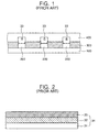
- FIG. 1 is a cross sectional view showing a structure of a conventional full color organic electroluminescence display device
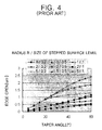
- FIG. 2 is a cross sectional view showing a structure of a conventional donor film for a laser induced thermal imaging method
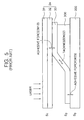
- FIG. 4 is a graph showing a relation between a stepped surface level generated by the pixel defining layer and the edge open defect as a relation between the size of the stepped surface level (i.e., the step height) and the radius of the curvature of an expansion part of a donor film;
- FIG. 7 is a graph showing energy transfer and the degree of energy absorption at respective positions of a light-to-heat conversion layer according to laser irradiation when the light-to-heat conversion layer is laid to a relatively large thickness of 4 ⁇ m when using a conventional donor film;
- FIG. 8 is a graph showing energy transfer and the degree of energy absorption at respective positions of the light-to-heat conversion layer according to laser irradiation when forming the light-to-heat conversion layer of a donor film as a preferred embodiment of the present invention to a thickness of 0.5 ⁇ m and using a metal layer;
- FIG. 9 is a drawing showing a structure of a donor film for a laser induced thermal imaging method according to a second preferred embodiment of the present invention.
- FIG. 10 is a drawing describing a method for laser induced thermal imaging using a donor film as a present invention.
- a first electrode 200 is patterned on an insulating substrate 100.
- the first electrode 200 is formed of a transparent electrode when the full color organic electroluminescence display device is a bottom emitting type.
- the first electrode 200 is formed of a conductive metal with a reflection film when the full color organic electroluminescence display device is a top emitting type.
- a pixel defining layer (PDL) 300 is formed of an insulating material on an upper part of the first electrode 200 to define a pixel region and to insulate an emitting layer from another emitting layer.
- a second electrode 400 is formed on the organic film layer 33.
- the second electrode 400 is formed of a conductive metal layer with the reflection film if the first electrode 200 is a transparent electrode, and the second electrode 400 is formed of a transparent electrode if the first electrode 200 is a conductive metal layer with the reflection film.
- An organic electroluminescence display device is completed by sealing the organic electroluminescence display device after forming the second electrode 400.
- a conventional donor film 34 for laser induced thermal imaging has a base film 31, the light-to-heat conversion layer 32 and transfer layer 33 and further has a buffer layer (not shown in FIG. 2) in case of forming an emitting layer using a conventional laser induced thermal imaging.
- the transfer layer 33 is not completely transferred because a stepped surface level exists on an edge part of the pixel region of the organic electroluminescence display device. This is called as an edge open defect or a non-transfer defect.
- the edge open defect is generated due to a large radius of the curvature made in a layer such as the light-to-heat conversion layer 32 or a buffer layer (not illustrated in FIG. 3) which is expanded by receiving laser energy. That is, the thick expanded part causes the edge open defect.
- the larger size of the stepped surface level the more edge open defects. Also, when the sizes of the stepped surface levels are equal, the larger radius of the curvature causes the more edge open defects.
- the edge open defect causes the deterioration of emission efficiency, life time and color characteristics of an organic electroluminescence display device.
- FIG. 5 is a drawing illustrating a transfer mechanism when transfer-patterning an organic emitting film used in an organic electroluminescence display device by using a laser according to the present invention.
- the first and second adhesive forces and tackiness are represented as the following expressions using surface tensions ⁇ 1 , ⁇ 2 and ⁇ 3 and interfacial tensions ⁇ 12 and ⁇ 23 of respective layers.
- the tackiness (W 22 ) of the film should be less than adhesive forces (W 12 , W 23 ) between the respective substrates and the film.
- the donor film of FIG. 6 can be changed according to its applications.
- the donor film further comprises a gas forming layer (not illustrated in FIG. 6) on either an upper part or a lower part of the light-to-heat conversion layer, and a buffer layer (not illustrated in FIG. 6) formed between the metal layer 35 and the transfer layer 33 to improve sensitivity of the film.
- the thickness of the light-to-heat conversion layer 32 is too thin, an energy absorption ratio is lowered so that expansion pressure is lowered due to low light-to-heat conversion energy, and transmission energy is increased so that substrate circuits of an organic electroluminescence display device are damaged.
- edge open defect caused by stepped surface level generated by a pixel defining layer is reduced by maintaining the light-to-heat conversion layer 32 to a certain thickness or less in order to decrease the radius of the curvature during expansion of the light-to-heat conversion layer 32.
- the thickness of the light-to-heat conversion layer 32 is too thick, there is a strong possibility of an edge open defect due to poor close adhesion between the film and the substrate at a part of the stepped surface level generated by a pixel defining layer.
- the light-to-heat conversion layer 32 is formed to a thickness of 100 to 5,000 ⁇ by vacuum deposition, electron beam deposition or sputtering if the light-to-heat conversion layer 32 is a metal, metal oxide or metal sulfide.
- the light-to-heat conversion layer 32 is laid to a thickness of 0.1 to 2 ⁇ m by a conventional film coating method of extrusion, gravure coating, spin coating or knife coating if the light-to-heat conversion layer 32 is an organic film.
- FIG. 7 is a graph showing energy transfer and the degree of energy absorption at respective positions of the light-to-heat conversion layer 32 according to laser irradiation when the light-to-heat conversion layer 32 is laid to a relatively large thickness of 4 ⁇ m when using a conventional donor film.
- the buffer layer and the transfer layer 33 is expanded although energy efficiency is good by absorbing most of the energy at a laser beam incidence part of the light-to-heat conversion layer and absorbing most of the energy while the energy is passing through the light-to-heat conversion layer.
- FIG. 8 is a graph showing energy transfer and the degree of energy absorption degree at respective positions of the light-to-heat conversion layer 32 according to laser irradiation when forming the light-to-heat conversion layer 32 of a donor film 34 according to a preferred embodiment of the present invention with a thickness of 0.5 ⁇ m and using the metal layer 35.
- energy absorbed into the light-to-heat conversion layer as passing through the light-to-heat conversion layer 32 according to laser irradiation is decreased since the thickness of the light-to-heat conversion layer is thinned.
- the light-to-heat conversion layer is easily closely adhered to the substrate even by small energy.
- the gas forming layer plays a role of providing transfer energy by generating decomposition reaction when light or heat is absorbed into the gas forming layer, thereby emitting nitrogen gas or hydrogen gas.
- the gas forming layer is formed of a material selected from pentaerythritol tetranitrate (PETN), trinitrotoluene (TNT), etc. Since the gas forming layer should receive heat from the light-to-heat conversion layer, the gas forming layer is formed adjacently to either an upper part or a lower part of the light-to-heat conversion layer or mixed with material of the light-to-heat conversion layer to form a single layer.
- PETN pentaerythritol tetranitrate
- TNT trinitrotoluene
- a metal having a laser beam transmittance of 20% or less is used as a metal layer 35 formed on an upper part of the light-to-heat conversion layer 32 over the base film. Furthermore, the metal layer 35 is laid to a thickness of 1 ⁇ m or less by vacuum deposition, electron beam deposition or sputtering. Thickness of the metal layer 35 is formed to such a degree that laser light is hardly transferred onto the substrate of an organic electroluminescence display device. If the metal layer is too thick, the characteristics of the laser induced thermal imaging may be affected because the metal layer is not expanded when the light-to-heat conversion layer is expanded.
- the metal layer not only prevents substrate circuits from being damaged, but also prevents gas generated in the light-to-heat conversion layer 32 from infiltrating into the transfer layer 33 since laser energy is not transferred to the substrate of an organic electroluminescence display device due to the metal layer during laser induced thermal imaging. Additionally, the metal layer 35 prevents thermal damage of the transfer layer by using a metal having high thermal conductivity to dissipate heat transferred to the transfer layer 33 from the light-to-heat conversion layer 32.
- a buffer layer (not illustrated in FIG. 8) can be further formed on an upper part of the metal layer 35.
- the buffer layer prevents metal from being diffused into the transfer layer and controls adhesive force of the metal layer with the transfer layer so that characteristics of transfer-patterns are improved.
- a metal oxide, metal sulfide, nonmetal inorganic compound or organic material can be used as the buffer layer.
- the metal oxide can be formed by oxidizing the surface of the metal layer or proceeding a separate process after forming a metal layer.
- the organic material may be formed by coating an inert polymer or depositing small molecules forms the organic material.
- the thickness of the buffer layer is preferably 0.01 to 2 ⁇ m.
- the laser is reflected by the metal layer 35 by introducing a metal layer 35 between the light-to-heat conversion layer 32 and the transfer layer 33 so that more energy is transferred to the light-to-heat conversion layer 32.
- FIG. 9 is a cross sectional view of a donor film for a laser induced thermal imaging method according to a second preferred embodiment of the present invention.
- the second preferred embodiment of the present invention displays the donor film for the laser induced thermal imaging method.
- the donor film is constructed with a base film 31, a light-to-heat conversion layer 32 and the transfer layer 33.
- the donor film further comprises a reflection layer 35' for reflecting an irradiated laser to the light-to-heat conversion layer 32 and preventing gas produced from the light-to-heat conversion layer 32 from infiltrating into the transfer layer 33.
- any materials such as organic material, inorganic material and metal can be used as the reflection layer if they are capable of preventing gas from infiltrating into the transfer layer.
- a metal selected from the group consisting of aluminum (Al), silver (Ag), chromium (Cr), tin (Sn), nickel (Ni), titanium (Ti), cobalt (Co), zinc (Zn), gold (Au), copper (Cu), tungsten (W), molybdenum (Mo) and lead (Pb) is used as the reflection layer.
- the reflection layer is preferably laid to a thickness of 1 ⁇ m or less considering gas infiltration blocking force and laser light transmittance of the reflection layer although the thickness of the reflection layer is varied depending on a material used as the reflection layer.
- a method for forming fine patterns on an organic thin film of an organic electroluminescence display device using a donor film according to the present invention referring to FIG. 10 is described in detail as follows.
- an organic electroluminescence display device is mentioned in the following description as one example to which a donor film of the present invention is applied for convenience of the description, application of the donor film of the present invention is not limited to the organic electroluminescence display device.
- a donor film for the laser induced thermal imaging method increases amount of energy absorbed into the light-to-heat conversion layer by forming a reflection layer or a metal layer between the light-to-heat conversion layer and the transfer layer, prevents damage of the substrate by not transmitting laser beam to the substrate and prevents deterioration of the transfer layer by preventing gas generated from the light-to-heat conversion layer by heat from penetrating into the transfer layer and dissipating heat transferred to the transfer layer.
Landscapes
- Engineering & Computer Science (AREA)
- Manufacturing & Machinery (AREA)
- Physics & Mathematics (AREA)
- Optics & Photonics (AREA)
- Electroluminescent Light Sources (AREA)
- Laminated Bodies (AREA)
- Thermal Transfer Or Thermal Recording In General (AREA)
- Physical Deposition Of Substances That Are Components Of Semiconductor Devices (AREA)
Applications Claiming Priority (2)
| Application Number | Priority Date | Filing Date | Title |
|---|---|---|---|
| KR2003094945 | 2003-12-22 | ||
| KR1020030094945A KR100579174B1 (ko) | 2003-12-22 | 2003-12-22 | 레이저 전사용 도너 필름 및 그 필름을 사용하여 제조되는유기 전계 발광 소자 |
Publications (2)
| Publication Number | Publication Date |
|---|---|
| EP1548857A1 true EP1548857A1 (de) | 2005-06-29 |
| EP1548857B1 EP1548857B1 (de) | 2008-03-19 |
Family
ID=34545890
Family Applications (1)
| Application Number | Title | Priority Date | Filing Date |
|---|---|---|---|
| EP04090480A Expired - Lifetime EP1548857B1 (de) | 2003-12-22 | 2004-12-06 | Verfahren zur Herstellung eines Musters einer organischen Dünnschicht für eine organische Elektrolumineszenzanzeigevorrichtung |
Country Status (7)
| Country | Link |
|---|---|
| US (1) | US20050136344A1 (de) |
| EP (1) | EP1548857B1 (de) |
| JP (1) | JP2005183381A (de) |
| KR (1) | KR100579174B1 (de) |
| CN (1) | CN1638543A (de) |
| AT (1) | ATE389953T1 (de) |
| DE (1) | DE602004012522T2 (de) |
Cited By (4)
| Publication number | Priority date | Publication date | Assignee | Title |
|---|---|---|---|---|
| WO2006033822A3 (en) * | 2004-09-07 | 2006-06-15 | Massachusetts Inst Technology | Fabrication of electronic and photonic systems on flexible substrates by layer transfer method |
| WO2011149813A1 (en) * | 2010-05-25 | 2011-12-01 | Eastman Kodak Company | Laser thermal donor elements and method of use |
| US8405909B2 (en) | 2008-05-09 | 2013-03-26 | Semiconductor Energy Laboratories Co., Ltd. | Deposition donor substrate and deposition method using the same |
| US8802185B2 (en) | 2008-05-29 | 2014-08-12 | Semiconductor Energy Laboratory Co., Ltd. | Deposition method and method for manufacturing light-emitting device |
Families Citing this family (46)
| Publication number | Priority date | Publication date | Assignee | Title |
|---|---|---|---|---|
| US7534543B2 (en) * | 1996-04-15 | 2009-05-19 | 3M Innovative Properties Company | Texture control of thin film layers prepared via laser induced thermal imaging |
| US7132140B2 (en) * | 2004-05-27 | 2006-11-07 | Eastman Kodak Company | Plural metallic layers in OLED donor |
| JP4615473B2 (ja) * | 2005-08-30 | 2011-01-19 | 三星モバイルディスプレイ株式會社 | レーザ熱転写装置及びこれを利用したレーザ熱転写法 |
| JP2007062354A (ja) | 2005-08-30 | 2007-03-15 | Samsung Sdi Co Ltd | レーザ熱転写ドナーフィルム、レーザ熱転写装置、レーザ熱転写法及び有機発光素子の製造方法 |
| US20070063205A1 (en) | 2005-08-30 | 2007-03-22 | Kang Tae M | Organic light emitting display device |
| KR100700822B1 (ko) * | 2005-08-30 | 2007-03-27 | 삼성에스디아이 주식회사 | 레이저 열 전사법 및 이를 이용한 유기 전계 발광 소자의제조방법 |
| US7817175B2 (en) | 2005-08-30 | 2010-10-19 | Samsung Mobile Display Co., Ltd. | Laser induced thermal imaging apparatus and fabricating method of organic light emitting diode using the same |
| KR100673758B1 (ko) * | 2005-09-13 | 2007-01-24 | 삼성에스디아이 주식회사 | 탈가스 포집부가 구비된 도너 필름 및 이의 제조방법 |
| KR100745332B1 (ko) * | 2005-09-28 | 2007-08-02 | 삼성에스디아이 주식회사 | 유기 발광표시장치 및 그 제조방법 |
| US7396631B2 (en) * | 2005-10-07 | 2008-07-08 | 3M Innovative Properties Company | Radiation curable thermal transfer elements |
| US7678526B2 (en) * | 2005-10-07 | 2010-03-16 | 3M Innovative Properties Company | Radiation curable thermal transfer elements |
| KR100635583B1 (ko) * | 2005-10-21 | 2006-10-18 | 삼성에스디아이 주식회사 | 유기 전계 발광 소자 및 그 제조 방법 |
| JP2007128845A (ja) | 2005-11-04 | 2007-05-24 | Samsung Sdi Co Ltd | レーザ熱転写装置及びレーザ熱転写方法 |
| JP2007128844A (ja) | 2005-11-04 | 2007-05-24 | Samsung Sdi Co Ltd | レーザ熱転写装置及びレーザ熱転写方法そしてこれを利用した有機発光表示素子 |
| KR100873071B1 (ko) * | 2005-11-07 | 2008-12-09 | 삼성모바일디스플레이주식회사 | 표면 균일도 향상을 위한 도너 필름 가공방법 |
| KR100700836B1 (ko) * | 2005-11-16 | 2007-03-28 | 삼성에스디아이 주식회사 | 레이저 열 전사 장치 및 레이저 열 전사법 그리고 이를이용한 유기 발광소자의 제조방법 |
| JP2007173145A (ja) * | 2005-12-26 | 2007-07-05 | Sony Corp | 転写用基板、転写方法、および有機電界発光素子の製造方法 |
| KR100793360B1 (ko) * | 2006-01-16 | 2008-01-11 | 삼성에스디아이 주식회사 | 레이저 조사 장치용 마스크 |
| KR100770264B1 (ko) | 2006-01-16 | 2007-10-25 | 삼성에스디아이 주식회사 | 레이저 조사 장치 및 이를 이용한 유기전계발광소자의제조방법 |
| KR100803214B1 (ko) * | 2006-06-28 | 2008-02-14 | 삼성전자주식회사 | 유기막을 채용한 전사필름 및 이를 이용한 금속막 형성방법 |
| KR100770272B1 (ko) * | 2006-07-04 | 2007-10-25 | 삼성에스디아이 주식회사 | 레이저 전사용 도너기판, 그의 제조방법 및 그를 이용한유기전계발광소자의 제조방법 |
| KR100770273B1 (ko) * | 2006-07-04 | 2007-10-25 | 삼성에스디아이 주식회사 | 도너기판 및 그의 제조방법 |
| KR100796594B1 (ko) * | 2006-07-04 | 2008-01-21 | 삼성에스디아이 주식회사 | 도너기판, 그의 제조방법 및 그를 이용한유기전계발광소자의 제조방법 |
| KR100731768B1 (ko) * | 2006-07-04 | 2007-06-22 | 삼성에스디아이 주식회사 | 도너 기판 및 그를 이용한 유기전계발광소자의 제조방법 |
| KR100731767B1 (ko) * | 2006-07-04 | 2007-06-22 | 삼성에스디아이 주식회사 | 도너 기판 및 그를 이용한 유기전계발광소자의 제조방법 |
| KR100832095B1 (ko) * | 2006-12-13 | 2008-05-27 | 삼성에스디아이 주식회사 | 레이저 열전사용 도너 기판 및 이를 이용한 레이저 열전사방법 |
| KR100900444B1 (ko) * | 2007-06-27 | 2009-06-02 | 엘지전자 주식회사 | 유기전계발광표시장치 및 그 제조방법 |
| KR100838088B1 (ko) | 2007-07-03 | 2008-06-16 | 삼성에스디아이 주식회사 | 유기 발광 소자 |
| KR100934262B1 (ko) | 2008-03-18 | 2009-12-28 | 삼성모바일디스플레이주식회사 | 유기전계발광표시장치 및 그의 제조방법 |
| US8182633B2 (en) * | 2008-04-29 | 2012-05-22 | Samsung Electronics Co., Ltd. | Method of fabricating a flexible display device |
| JP2010034007A (ja) * | 2008-07-31 | 2010-02-12 | Sony Corp | 転写シートおよび転写シートの形成方法 |
| KR101073559B1 (ko) | 2009-10-13 | 2011-10-17 | 삼성모바일디스플레이주식회사 | 도너 기판 및 그를 이용한 유기전계발광소자의 제조방법 |
| JP2011129345A (ja) * | 2009-12-17 | 2011-06-30 | Fujifilm Corp | 光熱変換シート、並びに、それを用いた有機電界発光素材シート、及び有機電界発光装置の製造方法 |
| JP5619461B2 (ja) * | 2010-03-31 | 2014-11-05 | ユー・ディー・シー アイルランド リミテッド | 光路長調整層転写シート、並びに有機電界発光装置及びその製造方法 |
| CN103620810B (zh) * | 2011-06-15 | 2016-04-13 | 可隆工业株式会社 | Liti施体膜 |
| KR101873037B1 (ko) * | 2011-10-27 | 2018-08-03 | 엘지디스플레이 주식회사 | 레이저 열전사기판 및 그 제조방법, 이를 이용한 유기전계발광소자의 제조방법 |
| KR101525999B1 (ko) | 2011-12-16 | 2015-06-04 | 제일모직주식회사 | 열전사 필름 |
| KR20140000565A (ko) | 2012-06-25 | 2014-01-03 | 삼성디스플레이 주식회사 | 도너 기판, 도너 기판을 이용한 레이저 열전사 방법 및 도너 기판을 이용한 유기 발광 표시 장치의 제조 방법 |
| EP2687380A3 (de) * | 2012-07-20 | 2017-10-11 | Cheil Industries Inc. | Wärmetransferfolie und organische elektrolumineszente Vorrichtung |
| KR20140107036A (ko) * | 2013-02-27 | 2014-09-04 | 삼성디스플레이 주식회사 | 유기 발광 표시 장치 및 그 제조 방법, 그리고 도너 기판 |
| KR20140139853A (ko) * | 2013-05-28 | 2014-12-08 | 삼성디스플레이 주식회사 | 도너기판 및 이를 이용한 전사패턴 형성방법 |
| KR101786151B1 (ko) * | 2013-09-27 | 2017-10-17 | 주식회사 엘지화학 | 불소계 수지를 포함하는 자외선 경화형 도너필름 조성물 및 이를 이용한 자외선 경화형 도너필름 |
| KR20150062090A (ko) * | 2013-11-28 | 2015-06-05 | 제일모직주식회사 | 열전사필름 및 이를 사용하여 제조된 유기전계발광소자 |
| JPWO2015152158A1 (ja) * | 2014-03-31 | 2017-04-13 | 株式会社Joled | 積層体および積層体の剥離方法ならびに可撓性デバイスの製造方法 |
| KR20160030002A (ko) * | 2014-09-05 | 2016-03-16 | 삼성디스플레이 주식회사 | 도너마스크 및 이를 이용한 유기발광 디스플레이 장치 제조방법 |
| KR102921492B1 (ko) * | 2021-05-06 | 2026-02-02 | 삼성디스플레이 주식회사 | 표시 장치의 제조장치 |
Citations (3)
| Publication number | Priority date | Publication date | Assignee | Title |
|---|---|---|---|---|
| EP0851714A2 (de) * | 1996-12-23 | 1998-07-01 | Samsung Display Devices Co., Ltd. | Donorfilm für organische dünne Schicht von elektrolumineszenter Vorrichtung, und Methode zur Herstellung der elektrolumineszenten Vorrichtung mit demselben |
| EP0858110A1 (de) * | 1996-08-27 | 1998-08-12 | Seiko Epson Corporation | Trennverfahren, verfahren zur übertragung eines dünnfilmbauelements, dünnfilmintegriertes schaltkreisbauelement und unter verwendung des übertragungsverfahrens hergestelltes flüssigkristall-anzeigebauelement |
| US20030124265A1 (en) * | 2001-12-04 | 2003-07-03 | 3M Innovative Properties Company | Method and materials for transferring a material onto a plasma treated surface according to a pattern |
Family Cites Families (15)
| Publication number | Priority date | Publication date | Assignee | Title |
|---|---|---|---|---|
| US5256506A (en) * | 1990-10-04 | 1993-10-26 | Graphics Technology International Inc. | Ablation-transfer imaging/recording |
| US5220348A (en) * | 1991-08-23 | 1993-06-15 | Eastman Kodak Company | Electronic drive circuit for multi-laser thermal printer |
| US5278023A (en) * | 1992-11-16 | 1994-01-11 | Minnesota Mining And Manufacturing Company | Propellant-containing thermal transfer donor elements |
| US5308737A (en) * | 1993-03-18 | 1994-05-03 | Minnesota Mining And Manufacturing Company | Laser propulsion transfer using black metal coated substrates |
| JPH09501620A (ja) * | 1993-08-13 | 1997-02-18 | レクスハム・グラフィクス・インコーポレーテッド | 中間レセプターへのアブレーション転写 |
| US5518861A (en) * | 1994-04-26 | 1996-05-21 | E. I. Du Pont De Nemours And Company | Element and process for laser-induced ablative transfer |
| US5521035A (en) * | 1994-07-11 | 1996-05-28 | Minnesota Mining And Manufacturing Company | Methods for preparing color filter elements using laser induced transfer of colorants with associated liquid crystal display device |
| US5688551A (en) * | 1995-11-13 | 1997-11-18 | Eastman Kodak Company | Method of forming an organic electroluminescent display panel |
| US5725989A (en) * | 1996-04-15 | 1998-03-10 | Chang; Jeffrey C. | Laser addressable thermal transfer imaging element with an interlayer |
| US5710097A (en) * | 1996-06-27 | 1998-01-20 | Minnesota Mining And Manufacturing Company | Process and materials for imagewise placement of uniform spacers in flat panel displays |
| US5998085A (en) * | 1996-07-23 | 1999-12-07 | 3M Innovative Properties | Process for preparing high resolution emissive arrays and corresponding articles |
| JP3809681B2 (ja) * | 1996-08-27 | 2006-08-16 | セイコーエプソン株式会社 | 剥離方法 |
| US5937272A (en) * | 1997-06-06 | 1999-08-10 | Eastman Kodak Company | Patterned organic layers in a full-color organic electroluminescent display array on a thin film transistor array substrate |
| US6114088A (en) * | 1999-01-15 | 2000-09-05 | 3M Innovative Properties Company | Thermal transfer element for forming multilayer devices |
| JP2002216957A (ja) | 2001-01-19 | 2002-08-02 | Sharp Corp | 転写法を用いた有機led表示パネルの製造方法およびそれにより製造された有機led表示パネル |
-
2003
- 2003-12-22 KR KR1020030094945A patent/KR100579174B1/ko not_active Expired - Fee Related
-
2004
- 2004-10-21 US US10/968,918 patent/US20050136344A1/en not_active Abandoned
- 2004-12-06 DE DE602004012522T patent/DE602004012522T2/de not_active Expired - Lifetime
- 2004-12-06 AT AT04090480T patent/ATE389953T1/de not_active IP Right Cessation
- 2004-12-06 EP EP04090480A patent/EP1548857B1/de not_active Expired - Lifetime
- 2004-12-10 JP JP2004358998A patent/JP2005183381A/ja active Pending
- 2004-12-22 CN CNA2004100820280A patent/CN1638543A/zh active Pending
Patent Citations (3)
| Publication number | Priority date | Publication date | Assignee | Title |
|---|---|---|---|---|
| EP0858110A1 (de) * | 1996-08-27 | 1998-08-12 | Seiko Epson Corporation | Trennverfahren, verfahren zur übertragung eines dünnfilmbauelements, dünnfilmintegriertes schaltkreisbauelement und unter verwendung des übertragungsverfahrens hergestelltes flüssigkristall-anzeigebauelement |
| EP0851714A2 (de) * | 1996-12-23 | 1998-07-01 | Samsung Display Devices Co., Ltd. | Donorfilm für organische dünne Schicht von elektrolumineszenter Vorrichtung, und Methode zur Herstellung der elektrolumineszenten Vorrichtung mit demselben |
| US20030124265A1 (en) * | 2001-12-04 | 2003-07-03 | 3M Innovative Properties Company | Method and materials for transferring a material onto a plasma treated surface according to a pattern |
Cited By (7)
| Publication number | Priority date | Publication date | Assignee | Title |
|---|---|---|---|---|
| WO2006033822A3 (en) * | 2004-09-07 | 2006-06-15 | Massachusetts Inst Technology | Fabrication of electronic and photonic systems on flexible substrates by layer transfer method |
| US8232182B2 (en) | 2004-09-07 | 2012-07-31 | Massachusetts Institute Of Technology | Fabrication of electronic and photonic systems on flexible substrates by layer transfer method |
| US9012992B2 (en) | 2004-09-07 | 2015-04-21 | Massachusetts Institute Of Technology | Fabrication of electronic and photonic systems on flexible substrates by layer transfer method |
| US8405909B2 (en) | 2008-05-09 | 2013-03-26 | Semiconductor Energy Laboratories Co., Ltd. | Deposition donor substrate and deposition method using the same |
| US8802185B2 (en) | 2008-05-29 | 2014-08-12 | Semiconductor Energy Laboratory Co., Ltd. | Deposition method and method for manufacturing light-emitting device |
| WO2011149813A1 (en) * | 2010-05-25 | 2011-12-01 | Eastman Kodak Company | Laser thermal donor elements and method of use |
| US8199176B2 (en) | 2010-05-25 | 2012-06-12 | Eastman Kodak Company | Laser thermal donor elements and method of use |
Also Published As
| Publication number | Publication date |
|---|---|
| KR20050063534A (ko) | 2005-06-28 |
| DE602004012522T2 (de) | 2009-05-07 |
| US20050136344A1 (en) | 2005-06-23 |
| JP2005183381A (ja) | 2005-07-07 |
| ATE389953T1 (de) | 2008-04-15 |
| CN1638543A (zh) | 2005-07-13 |
| EP1548857B1 (de) | 2008-03-19 |
| DE602004012522D1 (de) | 2008-04-30 |
| KR100579174B1 (ko) | 2006-05-11 |
Similar Documents
| Publication | Publication Date | Title |
|---|---|---|
| EP1548857B1 (de) | Verfahren zur Herstellung eines Musters einer organischen Dünnschicht für eine organische Elektrolumineszenzanzeigevorrichtung | |
| US20040191564A1 (en) | Donor film for low molecular weight full color organic electroluminescent device using laser induced thermal imaging method and method for fabricating low molecular weight full color organic electroluminescent device using the film | |
| KR100667067B1 (ko) | 레이저 전사용 도너 기판 및 그 기판을 사용하여 제조되는유기 전계 발광 소자 | |
| KR100694716B1 (ko) | 발광 중합체의 열 전사 | |
| KR100741582B1 (ko) | 물질의 열 패턴화에서의 전기적 활성 프라이머 층의 용도 | |
| JP5558594B2 (ja) | 有機発光ダイオードデバイスのためのパターニング及び処理方法 | |
| KR100195175B1 (ko) | 유기전자발광소자 유기박막용 도너필름, 이를 이용한 유기전자발광소자의 제조방법 및 그 방법에 따라 제조된 유기전자발광소자 | |
| KR20050037502A (ko) | 물질을 패턴에 따라 플라즈마 처리 표면에 전달하기 위한방법 및 물질 | |
| CN100576604C (zh) | 激光感应热成像方法的施主衬底及有机场致发光显示装置 | |
| KR100501315B1 (ko) | 레이저 전사법을 사용하는 저분자 풀칼라 유기 전계 발광소자용 도너 필름 및 그 필름을 사용하는 저분자 풀칼라유기 전계 발광 소자의 제조 방법 | |
| MXPA06006527A (es) | Transferencia termica de dendrimeros emisores de luz. | |
| WO2003017732A1 (en) | Method and materials for patterning of a polymerizable, amorphous matrix with electrically active material disposed therein | |
| US7625615B2 (en) | Donor substrate for full-color organic electroluminescent display device, method of manufacturing the same, and full-color organic electroluminescent display device using donor substrate | |
| US20050048316A1 (en) | Donor film for organic electroluminescent display device, method thereof, and organic electroluminescent display device using the same as donor film |
Legal Events
| Date | Code | Title | Description |
|---|---|---|---|
| PUAI | Public reference made under article 153(3) epc to a published international application that has entered the european phase |
Free format text: ORIGINAL CODE: 0009012 |
|
| 17P | Request for examination filed |
Effective date: 20041206 |
|
| AK | Designated contracting states |
Kind code of ref document: A1 Designated state(s): AT BE BG CH CY CZ DE DK EE ES FI FR GB GR HU IE IS IT LI LT LU MC NL PL PT RO SE SI SK TR |
|
| AX | Request for extension of the european patent |
Extension state: AL BA HR LV MK YU |
|
| AKX | Designation fees paid |
Designated state(s): AT BE BG CH CY CZ DE DK EE ES FI FR GB GR HU IE IS IT LI LT LU MC NL PL PT RO SE SI SK TR |
|
| 17Q | First examination report despatched |
Effective date: 20060529 |
|
| RTI1 | Title (correction) |
Free format text: METHOD FOR FORMING A PATTERN OF AN ORGANIC THIN FILM OF AN ORGANIC ELECTROLUMINESCENCE DISPLAY DEVICE |
|
| GRAP | Despatch of communication of intention to grant a patent |
Free format text: ORIGINAL CODE: EPIDOSNIGR1 |
|
| GRAS | Grant fee paid |
Free format text: ORIGINAL CODE: EPIDOSNIGR3 |
|
| GRAA | (expected) grant |
Free format text: ORIGINAL CODE: 0009210 |
|
| AK | Designated contracting states |
Kind code of ref document: B1 Designated state(s): AT BE BG CH CY CZ DE DK EE ES FI FR GB GR HU IE IS IT LI LT LU MC NL PL PT RO SE SI SK TR |
|
| REG | Reference to a national code |
Ref country code: GB Ref legal event code: FG4D |
|
| REG | Reference to a national code |
Ref country code: CH Ref legal event code: EP |
|
| REF | Corresponds to: |
Ref document number: 602004012522 Country of ref document: DE Date of ref document: 20080430 Kind code of ref document: P |
|
| REG | Reference to a national code |
Ref country code: IE Ref legal event code: FG4D |
|
| PG25 | Lapsed in a contracting state [announced via postgrant information from national office to epo] |
Ref country code: LT Free format text: LAPSE BECAUSE OF FAILURE TO SUBMIT A TRANSLATION OF THE DESCRIPTION OR TO PAY THE FEE WITHIN THE PRESCRIBED TIME-LIMIT Effective date: 20080319 Ref country code: FI Free format text: LAPSE BECAUSE OF FAILURE TO SUBMIT A TRANSLATION OF THE DESCRIPTION OR TO PAY THE FEE WITHIN THE PRESCRIBED TIME-LIMIT Effective date: 20080319 |
|
| PG25 | Lapsed in a contracting state [announced via postgrant information from national office to epo] |
Ref country code: AT Free format text: LAPSE BECAUSE OF FAILURE TO SUBMIT A TRANSLATION OF THE DESCRIPTION OR TO PAY THE FEE WITHIN THE PRESCRIBED TIME-LIMIT Effective date: 20080319 |
|
| NLV1 | Nl: lapsed or annulled due to failure to fulfill the requirements of art. 29p and 29m of the patents act | ||
| PG25 | Lapsed in a contracting state [announced via postgrant information from national office to epo] |
Ref country code: PL Free format text: LAPSE BECAUSE OF FAILURE TO SUBMIT A TRANSLATION OF THE DESCRIPTION OR TO PAY THE FEE WITHIN THE PRESCRIBED TIME-LIMIT Effective date: 20080319 Ref country code: BE Free format text: LAPSE BECAUSE OF FAILURE TO SUBMIT A TRANSLATION OF THE DESCRIPTION OR TO PAY THE FEE WITHIN THE PRESCRIBED TIME-LIMIT Effective date: 20080319 Ref country code: SI Free format text: LAPSE BECAUSE OF FAILURE TO SUBMIT A TRANSLATION OF THE DESCRIPTION OR TO PAY THE FEE WITHIN THE PRESCRIBED TIME-LIMIT Effective date: 20080319 |
|
| PG25 | Lapsed in a contracting state [announced via postgrant information from national office to epo] |
Ref country code: SE Free format text: LAPSE BECAUSE OF FAILURE TO SUBMIT A TRANSLATION OF THE DESCRIPTION OR TO PAY THE FEE WITHIN THE PRESCRIBED TIME-LIMIT Effective date: 20080619 Ref country code: CZ Free format text: LAPSE BECAUSE OF FAILURE TO SUBMIT A TRANSLATION OF THE DESCRIPTION OR TO PAY THE FEE WITHIN THE PRESCRIBED TIME-LIMIT Effective date: 20080319 Ref country code: PT Free format text: LAPSE BECAUSE OF FAILURE TO SUBMIT A TRANSLATION OF THE DESCRIPTION OR TO PAY THE FEE WITHIN THE PRESCRIBED TIME-LIMIT Effective date: 20080826 Ref country code: ES Free format text: LAPSE BECAUSE OF FAILURE TO SUBMIT A TRANSLATION OF THE DESCRIPTION OR TO PAY THE FEE WITHIN THE PRESCRIBED TIME-LIMIT Effective date: 20080630 Ref country code: SK Free format text: LAPSE BECAUSE OF FAILURE TO SUBMIT A TRANSLATION OF THE DESCRIPTION OR TO PAY THE FEE WITHIN THE PRESCRIBED TIME-LIMIT Effective date: 20080319 |
|
| PG25 | Lapsed in a contracting state [announced via postgrant information from national office to epo] |
Ref country code: NL Free format text: LAPSE BECAUSE OF FAILURE TO SUBMIT A TRANSLATION OF THE DESCRIPTION OR TO PAY THE FEE WITHIN THE PRESCRIBED TIME-LIMIT Effective date: 20080319 Ref country code: RO Free format text: LAPSE BECAUSE OF FAILURE TO SUBMIT A TRANSLATION OF THE DESCRIPTION OR TO PAY THE FEE WITHIN THE PRESCRIBED TIME-LIMIT Effective date: 20080319 |
|
| PG25 | Lapsed in a contracting state [announced via postgrant information from national office to epo] |
Ref country code: IS Free format text: LAPSE BECAUSE OF FAILURE TO SUBMIT A TRANSLATION OF THE DESCRIPTION OR TO PAY THE FEE WITHIN THE PRESCRIBED TIME-LIMIT Effective date: 20080719 |
|
| ET | Fr: translation filed | ||
| PLBE | No opposition filed within time limit |
Free format text: ORIGINAL CODE: 0009261 |
|
| STAA | Information on the status of an ep patent application or granted ep patent |
Free format text: STATUS: NO OPPOSITION FILED WITHIN TIME LIMIT |
|
| PG25 | Lapsed in a contracting state [announced via postgrant information from national office to epo] |
Ref country code: DK Free format text: LAPSE BECAUSE OF FAILURE TO SUBMIT A TRANSLATION OF THE DESCRIPTION OR TO PAY THE FEE WITHIN THE PRESCRIBED TIME-LIMIT Effective date: 20080319 |
|
| REG | Reference to a national code |
Ref country code: GB Ref legal event code: 732E |
|
| 26N | No opposition filed |
Effective date: 20081222 |
|
| PG25 | Lapsed in a contracting state [announced via postgrant information from national office to epo] |
Ref country code: BG Free format text: LAPSE BECAUSE OF FAILURE TO SUBMIT A TRANSLATION OF THE DESCRIPTION OR TO PAY THE FEE WITHIN THE PRESCRIBED TIME-LIMIT Effective date: 20080619 Ref country code: EE Free format text: LAPSE BECAUSE OF FAILURE TO SUBMIT A TRANSLATION OF THE DESCRIPTION OR TO PAY THE FEE WITHIN THE PRESCRIBED TIME-LIMIT Effective date: 20080319 |
|
| REG | Reference to a national code |
Ref country code: FR Ref legal event code: TP |
|
| PG25 | Lapsed in a contracting state [announced via postgrant information from national office to epo] |
Ref country code: MC Free format text: LAPSE BECAUSE OF NON-PAYMENT OF DUE FEES Effective date: 20081231 |
|
| REG | Reference to a national code |
Ref country code: CH Ref legal event code: PL |
|
| PG25 | Lapsed in a contracting state [announced via postgrant information from national office to epo] |
Ref country code: IT Free format text: LAPSE BECAUSE OF FAILURE TO SUBMIT A TRANSLATION OF THE DESCRIPTION OR TO PAY THE FEE WITHIN THE PRESCRIBED TIME-LIMIT Effective date: 20080319 |
|
| PG25 | Lapsed in a contracting state [announced via postgrant information from national office to epo] |
Ref country code: CY Free format text: LAPSE BECAUSE OF FAILURE TO SUBMIT A TRANSLATION OF THE DESCRIPTION OR TO PAY THE FEE WITHIN THE PRESCRIBED TIME-LIMIT Effective date: 20080319 |
|
| PG25 | Lapsed in a contracting state [announced via postgrant information from national office to epo] |
Ref country code: IE Free format text: LAPSE BECAUSE OF NON-PAYMENT OF DUE FEES Effective date: 20081208 Ref country code: CH Free format text: LAPSE BECAUSE OF NON-PAYMENT OF DUE FEES Effective date: 20081231 Ref country code: LI Free format text: LAPSE BECAUSE OF NON-PAYMENT OF DUE FEES Effective date: 20081231 |
|
| PG25 | Lapsed in a contracting state [announced via postgrant information from national office to epo] |
Ref country code: LU Free format text: LAPSE BECAUSE OF NON-PAYMENT OF DUE FEES Effective date: 20081206 Ref country code: HU Free format text: LAPSE BECAUSE OF FAILURE TO SUBMIT A TRANSLATION OF THE DESCRIPTION OR TO PAY THE FEE WITHIN THE PRESCRIBED TIME-LIMIT Effective date: 20080920 |
|
| PG25 | Lapsed in a contracting state [announced via postgrant information from national office to epo] |
Ref country code: TR Free format text: LAPSE BECAUSE OF FAILURE TO SUBMIT A TRANSLATION OF THE DESCRIPTION OR TO PAY THE FEE WITHIN THE PRESCRIBED TIME-LIMIT Effective date: 20080319 |
|
| PG25 | Lapsed in a contracting state [announced via postgrant information from national office to epo] |
Ref country code: GR Free format text: LAPSE BECAUSE OF FAILURE TO SUBMIT A TRANSLATION OF THE DESCRIPTION OR TO PAY THE FEE WITHIN THE PRESCRIBED TIME-LIMIT Effective date: 20080620 |
|
| REG | Reference to a national code |
Ref country code: DE Ref legal event code: R082 Ref document number: 602004012522 Country of ref document: DE Representative=s name: GULDE HENGELHAUPT ZIEBIG & SCHNEIDER, DE |
|
| REG | Reference to a national code |
Ref country code: DE Ref legal event code: R081 Ref document number: 602004012522 Country of ref document: DE Owner name: SAMSUNG DISPLAY CO., LTD., KR Free format text: FORMER OWNER: SAMSUNG MOBILE DISPLAY CO. LTD., SUWON, KR Effective date: 20121026 Ref country code: DE Ref legal event code: R082 Ref document number: 602004012522 Country of ref document: DE Representative=s name: GULDE HENGELHAUPT ZIEBIG & SCHNEIDER, DE Effective date: 20121026 Ref country code: DE Ref legal event code: R081 Ref document number: 602004012522 Country of ref document: DE Owner name: SAMSUNG DISPLAY CO., LTD., YONGIN-CITY, KR Free format text: FORMER OWNER: SAMSUNG MOBILE DISPLAY CO. LTD., SUWON, GYEONGGI, KR Effective date: 20121026 Ref country code: DE Ref legal event code: R082 Ref document number: 602004012522 Country of ref document: DE Representative=s name: GULDE & PARTNER PATENT- UND RECHTSANWALTSKANZL, DE Effective date: 20121026 |
|
| REG | Reference to a national code |
Ref country code: GB Ref legal event code: 732E Free format text: REGISTERED BETWEEN 20130103 AND 20130109 |
|
| REG | Reference to a national code |
Ref country code: FR Ref legal event code: TP Owner name: SAMSUNG DISPLAY CO., LTD., KR Effective date: 20130130 |
|
| PGFP | Annual fee paid to national office [announced via postgrant information from national office to epo] |
Ref country code: DE Payment date: 20141211 Year of fee payment: 11 Ref country code: GB Payment date: 20141211 Year of fee payment: 11 |
|
| PGFP | Annual fee paid to national office [announced via postgrant information from national office to epo] |
Ref country code: FR Payment date: 20141121 Year of fee payment: 11 |
|
| REG | Reference to a national code |
Ref country code: DE Ref legal event code: R119 Ref document number: 602004012522 Country of ref document: DE |
|
| GBPC | Gb: european patent ceased through non-payment of renewal fee |
Effective date: 20151206 |
|
| REG | Reference to a national code |
Ref country code: FR Ref legal event code: ST Effective date: 20160831 |
|
| PG25 | Lapsed in a contracting state [announced via postgrant information from national office to epo] |
Ref country code: DE Free format text: LAPSE BECAUSE OF NON-PAYMENT OF DUE FEES Effective date: 20160701 Ref country code: GB Free format text: LAPSE BECAUSE OF NON-PAYMENT OF DUE FEES Effective date: 20151206 |
|
| PG25 | Lapsed in a contracting state [announced via postgrant information from national office to epo] |
Ref country code: FR Free format text: LAPSE BECAUSE OF NON-PAYMENT OF DUE FEES Effective date: 20151231 |