EP1548844A1 - Filme mit mehrschichtiger heterostruktur, prozess zu ihrer herstellung und optische bauelemente damit - Google Patents
Filme mit mehrschichtiger heterostruktur, prozess zu ihrer herstellung und optische bauelemente damit Download PDFInfo
- Publication number
- EP1548844A1 EP1548844A1 EP03766748A EP03766748A EP1548844A1 EP 1548844 A1 EP1548844 A1 EP 1548844A1 EP 03766748 A EP03766748 A EP 03766748A EP 03766748 A EP03766748 A EP 03766748A EP 1548844 A1 EP1548844 A1 EP 1548844A1
- Authority
- EP
- European Patent Office
- Prior art keywords
- film
- organic layer
- substrate
- compound
- multilayer heterostructure
- Prior art date
- Legal status (The legal status is an assumption and is not a legal conclusion. Google has not performed a legal analysis and makes no representation as to the accuracy of the status listed.)
- Withdrawn
Links
Images


Classifications
-
- H—ELECTRICITY
- H10—SEMICONDUCTOR DEVICES; ELECTRIC SOLID-STATE DEVICES NOT OTHERWISE PROVIDED FOR
- H10K—ORGANIC ELECTRIC SOLID-STATE DEVICES
- H10K30/00—Organic devices sensitive to infrared radiation, light, electromagnetic radiation of shorter wavelength or corpuscular radiation
- H10K30/10—Organic devices sensitive to infrared radiation, light, electromagnetic radiation of shorter wavelength or corpuscular radiation comprising heterojunctions between organic semiconductors and inorganic semiconductors
- H10K30/15—Sensitised wide-bandgap semiconductor devices, e.g. dye-sensitised TiO2
- H10K30/151—Sensitised wide-bandgap semiconductor devices, e.g. dye-sensitised TiO2 the wide bandgap semiconductor comprising titanium oxide, e.g. TiO2
-
- H—ELECTRICITY
- H10—SEMICONDUCTOR DEVICES; ELECTRIC SOLID-STATE DEVICES NOT OTHERWISE PROVIDED FOR
- H10K—ORGANIC ELECTRIC SOLID-STATE DEVICES
- H10K30/00—Organic devices sensitive to infrared radiation, light, electromagnetic radiation of shorter wavelength or corpuscular radiation
- H10K30/20—Organic devices sensitive to infrared radiation, light, electromagnetic radiation of shorter wavelength or corpuscular radiation comprising organic-organic junctions, e.g. donor-acceptor junctions
-
- H—ELECTRICITY
- H10—SEMICONDUCTOR DEVICES; ELECTRIC SOLID-STATE DEVICES NOT OTHERWISE PROVIDED FOR
- H10K—ORGANIC ELECTRIC SOLID-STATE DEVICES
- H10K30/00—Organic devices sensitive to infrared radiation, light, electromagnetic radiation of shorter wavelength or corpuscular radiation
- H10K30/30—Organic devices sensitive to infrared radiation, light, electromagnetic radiation of shorter wavelength or corpuscular radiation comprising bulk heterojunctions, e.g. interpenetrating networks of donor and acceptor material domains
-
- H—ELECTRICITY
- H10—SEMICONDUCTOR DEVICES; ELECTRIC SOLID-STATE DEVICES NOT OTHERWISE PROVIDED FOR
- H10K—ORGANIC ELECTRIC SOLID-STATE DEVICES
- H10K30/00—Organic devices sensitive to infrared radiation, light, electromagnetic radiation of shorter wavelength or corpuscular radiation
- H10K30/50—Photovoltaic [PV] devices
-
- H—ELECTRICITY
- H10—SEMICONDUCTOR DEVICES; ELECTRIC SOLID-STATE DEVICES NOT OTHERWISE PROVIDED FOR
- H10K—ORGANIC ELECTRIC SOLID-STATE DEVICES
- H10K85/00—Organic materials used in the body or electrodes of devices covered by this subclass
- H10K85/10—Organic polymers or oligomers
- H10K85/111—Organic polymers or oligomers comprising aromatic, heteroaromatic, or aryl chains, e.g. polyaniline, polyphenylene or polyphenylene vinylene
- H10K85/114—Poly-phenylenevinylene; Derivatives thereof
-
- H—ELECTRICITY
- H10—SEMICONDUCTOR DEVICES; ELECTRIC SOLID-STATE DEVICES NOT OTHERWISE PROVIDED FOR
- H10K—ORGANIC ELECTRIC SOLID-STATE DEVICES
- H10K85/00—Organic materials used in the body or electrodes of devices covered by this subclass
- H10K85/30—Coordination compounds
- H10K85/311—Phthalocyanine
-
- Y—GENERAL TAGGING OF NEW TECHNOLOGICAL DEVELOPMENTS; GENERAL TAGGING OF CROSS-SECTIONAL TECHNOLOGIES SPANNING OVER SEVERAL SECTIONS OF THE IPC; TECHNICAL SUBJECTS COVERED BY FORMER USPC CROSS-REFERENCE ART COLLECTIONS [XRACs] AND DIGESTS
- Y02—TECHNOLOGIES OR APPLICATIONS FOR MITIGATION OR ADAPTATION AGAINST CLIMATE CHANGE
- Y02E—REDUCTION OF GREENHOUSE GAS [GHG] EMISSIONS, RELATED TO ENERGY GENERATION, TRANSMISSION OR DISTRIBUTION
- Y02E10/00—Energy generation through renewable energy sources
- Y02E10/50—Photovoltaic [PV] energy
- Y02E10/549—Organic PV cells
-
- Y—GENERAL TAGGING OF NEW TECHNOLOGICAL DEVELOPMENTS; GENERAL TAGGING OF CROSS-SECTIONAL TECHNOLOGIES SPANNING OVER SEVERAL SECTIONS OF THE IPC; TECHNICAL SUBJECTS COVERED BY FORMER USPC CROSS-REFERENCE ART COLLECTIONS [XRACs] AND DIGESTS
- Y02—TECHNOLOGIES OR APPLICATIONS FOR MITIGATION OR ADAPTATION AGAINST CLIMATE CHANGE
- Y02P—CLIMATE CHANGE MITIGATION TECHNOLOGIES IN THE PRODUCTION OR PROCESSING OF GOODS
- Y02P70/00—Climate change mitigation technologies in the production process for final industrial or consumer products
- Y02P70/50—Manufacturing or production processes characterised by the final manufactured product
-
- Y—GENERAL TAGGING OF NEW TECHNOLOGICAL DEVELOPMENTS; GENERAL TAGGING OF CROSS-SECTIONAL TECHNOLOGIES SPANNING OVER SEVERAL SECTIONS OF THE IPC; TECHNICAL SUBJECTS COVERED BY FORMER USPC CROSS-REFERENCE ART COLLECTIONS [XRACs] AND DIGESTS
- Y10—TECHNICAL SUBJECTS COVERED BY FORMER USPC
- Y10T—TECHNICAL SUBJECTS COVERED BY FORMER US CLASSIFICATION
- Y10T428/00—Stock material or miscellaneous articles
- Y10T428/24—Structurally defined web or sheet [e.g., overall dimension, etc.]
- Y10T428/24802—Discontinuous or differential coating, impregnation or bond [e.g., artwork, printing, retouched photograph, etc.]
- Y10T428/24893—Discontinuous or differential coating, impregnation or bond [e.g., artwork, printing, retouched photograph, etc.] including particulate material
- Y10T428/24901—Discontinuous or differential coating, impregnation or bond [e.g., artwork, printing, retouched photograph, etc.] including particulate material including coloring matter
Definitions
- the present invention relates to films having a multilayer heterostructure, optical devices using the same, and a process for producing the same, and more particularly to films having a multilayer heterostructure which are suitably applicable to optical devices such as reflection films, optical filters, optical resonators, EL (electroluminescent) devices, display devices and optical sensors, and a process for producing these films having a multilayer heterostructure which are formable over a large surface area of a substrate.
- Films having a multilayer heterostructure have such a structure that different kinds of materials are alternately laminated on each other, and suitably used as optical reflection films and optical transmission films as well as optical devices such as optical resonators, EL devices, display devices and optical sensors because of various optical properties thereof.
- the respective layers of the films having a multilayer heterostructure are different in refractive index from each other since these layers are made of the different kinds of materials, so that reflection or refraction phenomenon occurs at boundary surfaces therebetween. Therefore, the change or modification in materials, thicknesses or number of the respective layers enables production of thin films having various optical properties.
- Japanese Patent Application Laid-open No. 2001-350015 has proposed films having a multilayer heterostructure which are formed by alternately laminating a first layer obtained by a sol-gel method and a second layer obtained by an alternate adsorption method.
- An object of the present invention is to provide films having a multilayer heterostructure which are produced by improving the techniques described in Japanese Patent Application Laid-open No. 2001-350015, and exhibit advanced functions.
- the present invention has been accomplished on the basis of the above finding.
- the film having a multilayer heterostructure according to the present invention is characterized in that the film includes at least one organic layer formed by self-assembly, and the organic layer contains a sensitizing dye.
- the film having a multilayer heterostructure according to the present invention is also characterized in that the film include at least one organic layer and at least one inorganic layer each formed by self-assembly, and the organic layer contains an aromatic compound.
- the sensitizing dye used herein means such a dye capable of increasing a sensitivity to light even when added in a small amount, namely enhancing a photoelectric effect.
- the sensitizing dye to be added to the organic layer preferably exhibits light absorption in a visible light range.
- Specific examples of the sensitizing dye include phthalocyanine-based compounds, porphyrin-based compounds, rhodamine-based compounds, perylene-based compounds, cyanine-based compounds, merocyanine-based compounds and xanthene-based compounds. Of these compounds, preferred are phthalocyanine-based compounds, and most preferred is copper phthalocyanine since this compound has a maximum absorption in a wavelength range of 600 to 700, and is inexpensive.
- the amount of the sensitizing dye added is in the range of 0.001 to 100 mM and preferably 1 to 10 mM in view of effects attained by the addition thereof.
- the "self-assembly” used herein means a method for forming a film owing to a self-assembling nature of molecules, etc., due to attraction forces such as electrostatic attraction force, so that organic substances and/or inorganic substances are self-assembled and formed into a thin film. More specifically, as the self-assembly method, there are known alternate adsorption method, sol-gel method, chemical solution precipitation method, in-situ polymerization method (polymerization adsorption method), Langmuir-Blodgeti method, etc. In the present invention, it is preferred that the organic layer is formed by alternate adsorption method, and the inorganic layer is formed by sol-gel method.
- the alternate adsorption method means such a technique in which a substrate is alternately dipped in a solution containing positively-charged particles and a solution containing negatively-charged particles to form a thin film having a multilayer structure.
- the surface of the substrate is first subjected to hydrophilic treatment to introduce OH- groups thereinto, thereby imparting negative charges as initial surface charges thereto.
- the substrate having the thus negatively charged surface is dipped in the solution containing positively-charged particles to adsorb the positively-charged particles onto the surface of the substrate by Coulomb's force therebetween, so that the positively charged particles adsorbed are formed into a thin film on the surface of the substrate.
- the thus treated substrate is dipped in the solution containing negatively-charged particles to form the negatively-charged particles into a layer-like thin film on an outside of the thin film composed of the positively-charged particles.
- These procedures are alternately repeated to form a composite thin film having a multilayer structure in which the thin film made of the positively-charged particles and the thin film made of the negatively-charged particles are alternately laminated on the substrate.
- the organic layer preferably contains an aromatic compound. More preferably, the aromatic compound is used as the positively-charged particles.
- the organic layer containing the aromatic compound has advantages such as good absorptivity to ultraviolet rays, visible lights and infrared rays, good electric conductivity and emission of fluorescence and phosphor.
- the aromatic compound used herein means a high-molecular compound mainly having an aromatic ring.
- Specific examples of the aromatic compound include poly-p-phenylene vinylene and precursors thereof such as acid salts of poly(xylydene-tetrahydrothiophenium), polyaniline, polypyrrole, polythiophene, poly-p-phenylene and polypyridine. Of these aromatic compounds, especially preferred are acid salts of poly(xylydene-tetrahydrothiophenium), polyaniline and polypyrrole.
- the negatively-charged particles used in the present invention are not particularly limited as long as they are capable of alternate adsorption with the positively-charged particles.
- the preferred negatively-charged particles include high-molecular compounds having a carboxyl group. Specific examples of such high-molecular compounds include polyacrylic acid and polymethacrylic acid.
- the alternate adsorption conditions such as particle concentrations of the solutions containing the positively-charged particles and the negatively-charged particles, respectively, pH thereof upon the treatment, and adsorption time may be appropriately determined according to film thickness, functions to be imparted to the film, etc.
- the substrate is alternately dipped in the solution containing the positively-charged particles and the solution containing the negatively-charged particles, these solutions tend to be contaminated.
- the substrate is preferably subjected to a rinsing step between the respective steps of dipping the substrate in the solution containing the positively-charged particles and the solution containing the negatively-charged particles.
- the film having a multilayer structure according to the present invention preferably further comprises at least one inorganic layer formed by self-assembly in addition to the above organic layer.
- the self-assembly of the inorganic layer is preferably conducted by sol-gel method.
- the sol-gel method used herein generally means such a method in which a solution containing an organic or inorganic metal compound is subjected to hydrolysis or polycondensation reaction of the compound to convert the sol into a gel, and then the resultant gel is dried to obtain a solid metal oxide.
- the surface of the substrate is also first covered with a specific reactive group (e.g., OH- groups). Then, the substrate is dipped in an aqueous solution containing a metal compound to be adsorbed onto the substrate, thereby allowing the metal or the metal compound to be chemically adsorbed to the reactive groups present on the surface of the substrate. Next, the metal compound adsorbed onto the surface of the substrate is hydrolyzed and converted into a sol state. Thereafter, the surface of the substrate is dried to convert the metal compound in the form of sol into a gel state and further convert the gel into a solid metal compound.
- a specific reactive group e.g., OH- groups
- a rinsing step for the substrate is preferably conducted between the chemical adsorption step and the hydrolysis step for the purpose of removing an excess amount of the metal compound attached to the surface of the substrate.
- a solution containing a metal alkoxide there may be frequently used a solution containing a metal alkoxide.
- a metal alkoxide is a metal compound represented by the chemical formula: M(OR) n wherein M is metal; and R is an alkyl group.
- M is metal
- R is an alkyl group.
- Specific examples of the metal M include titanium, silicon, zirconium, aluminum, barium, lithium, niobium, potassium, tantalum, indium, tin, sodium and boron. These metals may be used singly or in combination of any two or more thereof.
- metal alkoxides containing the combination of metals examples include alkoxides of indium-tin, boron-silicon, silicon-titanium, etc.
- the use of metal alkoxides containing titanium as M is preferred, and the inorganic layer is preferably in the form of a thin film containing titanium oxide.
- the film having a multilayer heterostructure according to the present invention is produced by alternately subjecting the same substrate to the step of forming mainly the organic layer, for example, by alternate adsorption method and the step of forming mainly the inorganic layer, for example, by sol-gel method.
- the layer to be first formed and the method used therefor as well as the layer to be last formed and the method therefor are optional, and may be appropriately determined according to kind of the aimed film having a multilayer heterostructure and functions to be imparted thereto.
- the film-forming step by alternate adsorption method is shifted to the film-forming step by sol-gel method and vice versa, it is preferred that a desired amount of electric charges still remain on the surface of the substrate. This is because the step of introducing OH - groups into the surface of the substrate before forming the respective layers can be omitted to thereby simplify the respective steps.
- the film having a multilayer heterostructure according to the present invention is applicable to reflection films and transmission films as well as other optical devices.
- the film having a multilayer heterostructure whose organic layer contains the aromatic compound and the sensitizing dye may be suitably applied to photoelectric devices.
- the film having a multilayer heterostructure which includes at least one organic layer containing an aromatic compound and at least one inorganic layer which layers are respectively formed by self assembly is effectively applied to optical devices such as optical resonators, EL devices, display devices and optical sensors.
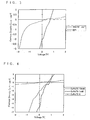
- Example 1 From Fig. 1, it was confirmed that the organic thin film obtained in Example 1 exhibited a maximum absorption attributed to CuPcTS at a wavelength near 620 nm in addition to the spectrum attributed to PPV. In addition, the visual observation showed that the organic thin film had a blue color due to CuPcTS, and no yellowish green fluorescence due to PPV was observed.
- Example 1 Short circuit current Jsc ( ⁇ A ⁇ cm -1 ) 5.82 2.08 Release voltage Voc (mV) 831 638 Curve factor FF 0.150 0.247 Conversion efficiency ⁇ (%) 0.000751 0.000328
- the respective steps of forming the organic and inorganic layers were repeated four times, thereby producing the ITO substrate formed thereon with the thin film having such a structure represented by ITO/(PPV/SPS) 5 /(PPV/PAA) 10 /TiO 2 ) 4 .
- the film having a multilayer heterostructure according to the present invention can be readily formed over a large surface area, and can be applied to various optical devices owing to its good photoelectric effect.
Landscapes
- Physics & Mathematics (AREA)
- Electromagnetism (AREA)
- Chemical & Material Sciences (AREA)
- Inorganic Chemistry (AREA)
- Laminated Bodies (AREA)
Applications Claiming Priority (5)
| Application Number | Priority Date | Filing Date | Title |
|---|---|---|---|
| JP2002228582 | 2002-08-06 | ||
| JP2002228583 | 2002-08-06 | ||
| JP2002228582 | 2002-08-06 | ||
| JP2002228583 | 2002-08-06 | ||
| PCT/JP2003/009935 WO2004013914A1 (ja) | 2002-08-06 | 2003-08-05 | 多層ヘテロ構造膜、その製造方法及びこれを用いた光学素子 |
Publications (2)
| Publication Number | Publication Date |
|---|---|
| EP1548844A1 true EP1548844A1 (de) | 2005-06-29 |
| EP1548844A4 EP1548844A4 (de) | 2010-11-03 |
Family
ID=31497641
Family Applications (1)
| Application Number | Title | Priority Date | Filing Date |
|---|---|---|---|
| EP03766748A Withdrawn EP1548844A4 (de) | 2002-08-06 | 2003-08-05 | Filme mit mehrschichtiger heterostruktur, prozess zu ihrer herstellung und optische bauelemente damit |
Country Status (5)
| Country | Link |
|---|---|
| US (1) | US20060110585A1 (de) |
| EP (1) | EP1548844A4 (de) |
| JP (1) | JPWO2004013914A1 (de) |
| AU (1) | AU2003254813A1 (de) |
| WO (1) | WO2004013914A1 (de) |
Family Cites Families (11)
| Publication number | Priority date | Publication date | Assignee | Title |
|---|---|---|---|---|
| JPH01209768A (ja) * | 1988-02-18 | 1989-08-23 | Canon Inc | 有機太陽電池 |
| JPH0832320B2 (ja) * | 1990-01-30 | 1996-03-29 | 出光興産株式会社 | 薄膜の製造方法 |
| JP2969902B2 (ja) * | 1990-10-17 | 1999-11-02 | 三菱化学株式会社 | 有機薄膜 |
| US5217792A (en) * | 1991-10-17 | 1993-06-08 | At&T Bell Laboratories | Stable polar optically nonlinear multilayer films and devices using the same |
| US5518767A (en) * | 1993-07-01 | 1996-05-21 | Massachusetts Institute Of Technology | Molecular self-assembly of electrically conductive polymers |
| JP2966795B2 (ja) * | 1996-09-30 | 1999-10-25 | 科学技術振興事業団 | 機能性薄膜とその製造方法 |
| JPH10180933A (ja) * | 1996-12-27 | 1998-07-07 | Toyota Central Res & Dev Lab Inc | 無機−有機層状高分子単層膜およびその多層積層膜 |
| JP4505604B2 (ja) * | 2000-06-09 | 2010-07-21 | 学校法人慶應義塾 | 多層ヘテロ構造膜およびこれを用いた光学素子ならびにその製造方法 |
| US6586791B1 (en) * | 2000-07-19 | 2003-07-01 | 3M Innovative Properties Company | Transistor insulator layer incorporating superfine ceramic particles |
| JP2002094085A (ja) * | 2000-09-13 | 2002-03-29 | Kyocera Corp | 有機太陽電池 |
| DE60033038T2 (de) * | 2000-11-24 | 2007-08-23 | Sony Deutschland Gmbh | Hybridsolarzelle mit thermisch abgeschiedener Halbleiteroxidschicht |
-
2003
- 2003-08-05 AU AU2003254813A patent/AU2003254813A1/en not_active Abandoned
- 2003-08-05 JP JP2004525838A patent/JPWO2004013914A1/ja active Pending
- 2003-08-05 EP EP03766748A patent/EP1548844A4/de not_active Withdrawn
- 2003-08-05 WO PCT/JP2003/009935 patent/WO2004013914A1/ja not_active Ceased
- 2003-08-05 US US10/523,369 patent/US20060110585A1/en not_active Abandoned
Also Published As
| Publication number | Publication date |
|---|---|
| JPWO2004013914A1 (ja) | 2006-09-28 |
| AU2003254813A1 (en) | 2004-02-23 |
| EP1548844A4 (de) | 2010-11-03 |
| AU2003254813A8 (en) | 2004-02-23 |
| US20060110585A1 (en) | 2006-05-25 |
| WO2004013914A1 (ja) | 2004-02-12 |
Similar Documents
| Publication | Publication Date | Title |
|---|---|---|
| KR101056440B1 (ko) | 염료감응 태양전지 | |
| JP5877149B2 (ja) | 色素増感光電池のための金属基板 | |
| US20120267240A1 (en) | Photoelectrode with a polymer layer | |
| KR20110137367A (ko) | 광학 코팅 | |
| EP2720285B1 (de) | Verfahren zur Herstellung eines gemusterten Substrats | |
| US20090320894A1 (en) | Method for preparing nanocrystalline transparent films of tungsten oxide | |
| CN106953013B (zh) | 一种双面光响应钙钛矿太阳能电池及其制备方法 | |
| JP2002134178A (ja) | 光電気セル | |
| JP2008277019A (ja) | 光電気セルおよび該光電気セル用多孔質半導体膜形成用塗料 | |
| CN111554815A (zh) | 一种窄带多光谱钙钛矿光电探测器及其制备方法和用途 | |
| CN115377297B (zh) | 一种提升钙钛矿太阳能电池性能的方法 | |
| CN111430480A (zh) | 一种同质结钙钛矿光电探测器及其制备方法和用途 | |
| CN112563419B (zh) | 一种非铅双钙钛矿太阳能电池及其制备方法 | |
| JP4310961B2 (ja) | 色素増感太陽電池 | |
| WO1993020569A1 (en) | Photovoltaic cells | |
| JP5580325B2 (ja) | 色素増感光電セル | |
| JP4916683B2 (ja) | 光電気セル | |
| KR101680053B1 (ko) | 다공질 반도체막 형성용 도료 및 광전기 셀 | |
| CN112567545A (zh) | 包括发光太阳能集中器和基于钙钛矿的光伏电池的光伏装置 | |
| Huang et al. | Multifunctional all-TiO2 Bragg stacks based on blocking layer-assisted spin coating | |
| US20060110585A1 (en) | Films having multilayer heterostructure, process for producing the same and optical devices using the same | |
| US20060162769A1 (en) | Low-temperature metal oxide coating | |
| JP2003092417A (ja) | 光電変換素子 | |
| KR101876575B1 (ko) | 전자수송용 산화티타늄층 | |
| JP2003264304A (ja) | 光電変換素子 |
Legal Events
| Date | Code | Title | Description |
|---|---|---|---|
| PUAI | Public reference made under article 153(3) epc to a published international application that has entered the european phase |
Free format text: ORIGINAL CODE: 0009012 |
|
| 17P | Request for examination filed |
Effective date: 20050215 |
|
| AK | Designated contracting states |
Kind code of ref document: A1 Designated state(s): AT BE BG CH CY CZ DE DK EE ES FI FR GB GR HU IE IT LI LU MC NL PT RO SE SI SK TR |
|
| AX | Request for extension of the european patent |
Extension state: AL LT LV MK |
|
| DAX | Request for extension of the european patent (deleted) | ||
| RBV | Designated contracting states (corrected) |
Designated state(s): DE FR GB |
|
| A4 | Supplementary search report drawn up and despatched |
Effective date: 20101001 |
|
| 17Q | First examination report despatched |
Effective date: 20110202 |
|
| STAA | Information on the status of an ep patent application or granted ep patent |
Free format text: STATUS: THE APPLICATION IS DEEMED TO BE WITHDRAWN |
|
| 18D | Application deemed to be withdrawn |
Effective date: 20110614 |